ACTIVATION OF CdTe SOLAR CELLS USING MOLECULAR CHLORINE
by
ii
A thesis submitted to the Faculty and Board of Trustees of the Colorado School of Mines in partial fulfillment of the requirements for the degree of Master of Science (Chemical Engineering). Golden, Colorado Date _________________________ Signed: _________________________ Jason R. Trevithick Signed: _________________________ Dr. Colin A. Wolden Thesis Advisor Golden, Colorado Signed: _________________________ Signed: _________________________ Dr. David W.M. Marr Professor and Head Chemical and Biological Engineering Department
iii ABSTRACT
Cadmium telluride-based photovoltaics are presently the leading commercialized thin film solar cell technology. A critical step during device fabrication is exposure of the as-deposited CdTe absorber to CdCl2 vapor at ~400 ºC for 10 – 30 min. This step is critical for obtaining high power conversion efficiencies and has been correlated with recrystallization and grain growth, passivation of grain boundaries, and heterojunction interdiffusion. This activation step is difficult to control and capex intensive. In addition, the use of CdCl2 presents a significant environmental concern due to its high solubility in water. In this thesis we explored molecular chlorine (Cl2) as an alternative to CdCl2 for activation of CdTe solar cells. This activation treatment could potentially serve as a direct replacement for CdCl2 processing in commercial module manufacturing.
Molecular Cl2 diluted in N2/O2 mixtures was exposed to as-deposited
FTO/CdS/CdTe stacks in a custom-built quartz tube furnace, enabling independent control of Cl2/Ar flowrate (1 – 5 sccm), temperature (375 – 420 ºC), oxygen
concentration (0 – 25 %), and treatment time (0 – 10 min). The (111) texture coefficient was tracked during experiments to measure extents of recrystallization as parameters were explored, followed by correlations with device performance. Within the parameters explored it was found that a threshold temperature of T ≥ 400 ºC was required for
recrystallization of the films. This coincides with the typical optimum temperature used for CdCl2 activation. In stark contrast to CdCl2 activation, very short treatment times (~1 min) and no oxygen ambient were needed for optimal device performance. In addition, the Cl2 process delivered significantly improved uniformity and run to run reproducibility relative to conventional CdCl2 activation. The Cl2 process also displayed a much larger
iv
process window with respect to temperature and eliminated delamination. A final optimization of 1.5 sccm of 3% Cl2/Ar, T = 415 ºC, 800 sccm N2, and 2 min resulted in an 11.6% efficient device with an open circuit voltage > 800 mV. This value surpasses the best reports in the literature (9-10 %) and exceeds that of many alternative
activation agents (HCl, NaCl, etc.).
Best device performance was less than the 14.5% baseline efficiency achieved with standard CdCl2 treatment. Device characterization revealed losses in both Voc (~50 mV) and Jsc (2-3 mA/cm2). Quantum efficiency showed that collection in the bulk CdTe region was 10% lower than standard CdCl2 activation, suggesting defect-based bulk recombination. Transmission electron microscopy and elemental mapping revealed that grain coalescence was incomplete under Cl2 activation, leaving regions with voids or low density. Both chlorine and oxygen accumulate at these defects, explaining the substandard performance. The optimal chlorine exposure was the lowest that could be reliably delivered, and it is recommended that further studies reduce the Cl2
concentration by an order of magnitude or more. In addition, longer times may be required to improve grain coalescence and extend interdiffusion at the heterojunction. The source of oxygen impurities is unclear and requires further investigation.
Nevertheless these initial studies are quite promising and a pathway is provided to further improve Cl2 activation and enable its use as a cost-effective alternative to conventional CdCl2.
v TABLE OF CONTENTS ABSTRACT...iii LIST OF FIGURES...vii LIST OF TABLES...xi ACKNOWLEDGEMENTS...xii CHAPTER 1 INTRODUCTION...1
1.1 The Terawatt Challenge...1
1.2 Photovoltaic Basics...3
1.3 Solar Cell Technologies...10
1.4 Thin Film CdTe Solar Cells...12
1.5 CdTe Activation...18
CHAPTER 2 EXPERIMENTAL METHODS...27
2.1 Substrate Preparation...27
2.2 CdS Thermal Evaporation...28
2.3 CdTe Vapor Transport Deposition...29
2.4 Chlorine Activation...32
2.5 ZnTe:Cu Contacts...38
2.6 X-ray diffraction...42
vi
CHAPTER 3 RESULTS AND DISCUSSION...47
3.1 Activation of CdTe Solar Cells Using Molecular Chlorine...47
3.2 Introduction...47
3.3 Experimental...49
3.4 Results and Discussion...50
3.5 Conclusions...61
CHAPTER 4 ADDITIONAL AND PRELIMINARY RESULTS...62
4.1 Results from Devices Processed in Excess O2/Cl2 ...62
4.2 Attempts to Reduce Cl2 Exposure...65
4.3 TEM Analysis...66
4.4 Sources of Unintentional Oxygen...70
4.5 Investigations of Interdiffusion...71
CHAPTER 5 SUMMARY AND CONCLUSIONS...74
5.1 Summary...74
5.2 Recommendations for future work...77
vii
LIST OF FIGURES
Figure 1.1 Approximately linear relationship between global warming and atmospheric CO2. The blue region represents one standard
deviation of uncertainty...2
Figure 1.2 Band diagrams of an (a) insulator, (b) semiconductor, and (c) metal...4
Figure 1.3 Band diagram of an (a) extrinsic and (b) p-type semiconductor...5
Figure 1.4 Depletion region of a p-n junction...6
Figure 1.5 Band bending in a p-n junction...7
Figure 1.6 Equivalent circuit of a solar cell...8
Figure 1.7 J-V characteristics of a 13 % solar cell...9
Figure 1.8 Solar cell efficiency as a function bandgap for terrestrial illumination...10
Figure 1.9 CdTe Superstrate Configuration...13
Figure 1.10 Hexagonal wurtzite (a) and (b) cubic zincblende structures...14
Figure 1.11 Vapor pressure data for absorber and window layer components...15
Figure 1.12 AFM images of CdTe treated with (a) HCF2Cl at 420 ºC and (b) CdCl2 at 410 ºC showing similar 2 µm diameter grains. The CdCl2 has been etched...22
viii
Figure 1.13 XRD data for (A) 10 mbar HCF2Cl/50 mbar Ar and (B) 10 mbar
HCF2Cl...22
Figure 2.1 Schematic diagram of TEC 15 glass...27
Figure 2.2 Glass/FTO/CdS Stack...28
Figure 2.3 Thermal evaporator diagram...30
Figure 2.4 Glass/FTO/CdS/CdTe stack...31
Figure 2.5 VTD system image...33
Figure 2.6 VTD schematic diagram...34
Figure 2.7 Cl2 Tube Furnace...36
Figure 2.8 Schematic of completed devices (a) and corresponding image of completed devices (b)...39
Figure 2.9 Addition of a baffle for co-evaporation...40
Figure 2.10 Rapid Thermal Processing (RTP)...41
Figure 2.11 Bragg’s Law...42
Figure 2.12 Standard 20 – 80º XRD scans of activated samples...44
Figure 3.1 (a) normalized XRD patterns and (b) resulting (111) texture coefficient as a function of process temperature at t = 10 min, 25% O2, 5 sccm Cl2/Ar...52
Figure 3.2 TC(111) as a function of Cl2/Ar flowrate at T = 400 ºC, t = 10 min, and 25% O2...53
ix
Figure 3.3 (a) Representative J-V curves and (b) box plots summarizing device efficiency as a function of Cl2/Ar flowrate at at T = 400 ºC, t = 10 min, and 25% O2...54
Figure 3.4 (111) texture coefficient as a function of time at T = 400 ºC, t = 2 min, and 1.5 sccm Cl2/Ar...55
Figure 3.5 TC(111) as a function of oxygen fraction at T = 400 ºC, t = 2 min, and 1.5 sccm Cl2/Ar...55
Figure 3.6 (a) Representative J-V curves and (b) box plots summarizing device efficiency as a function of oxygen content at T = 400 ºC, t = 2 min, and 1.5 sccm
Cl2/Ar...56
Figure 3.7 Device efficiency as a function of process temperature using 1.5 sccm Cl2/Ar, 0% O2, and a treatment time of 2 min...57
Figure 3.8 Comparison of (a) carrier concentration profiles and (b) EQE curves for Cl2 activated devices at 400 ºC and 405 ºC with a
standard CdCl2 device...58
Figure 3.9 Comparison of J-V curves obtained using standard CdCl2
activation and molecular Cl2 activation...60
Figure 4.1 Box plots summarizing efficiency results for an initial
temperature optimization at t = 10 min, 25% O2, 5 sccm Cl2/Ar...63
Figure 4.2 Planar FE-SEM images of an CdTe (a) as-deposited and after Cl2 activation using (b) 1 sccm, and (c) 5 sccm of Cl2/Ar
mixture...64
Figure 4.3 Comparison of a 1 min and 2 min activated device...65
Figure 4.4 BF-TEM images of an (a) un-activated, (b) a CdCl2 treated, and (c) a Cl2 treated device...67
x
Figure 4.5 Cl EDX maps of (a) a CdCl2 and (b) Cl2 activated device...68
Figure 4.6 O EDX maps for (a) CdCl2 device and (b) Cl2– activated device. (c) Cl EDX map for comparison...69
Figure 4.7 High resolution (a) oxygen, (b) chlorine, and (c) tellurium EDX maps from a Cl2 – activated device near the back contact...69
xi
LIST OF TABLES
Table 1.1 Performance results for device activated with non-cadmium
containing salts...24
Table 1.2 Texture coefficients for various activation salts at optimal conditions...25
Table 2.1 Quartz Tube Specifications...35
Table 2.2 Studied conditions of Cl2 tube furnace...38
Table 2.3 Post-processed XRD data suitable for TC analysis...44
Table 4.1 Relevant data from the deconvolution of the CdTe and CdSxTe1-x (422) peaks...73
xii
ACKNOWLEDGEMENTS
I am most grateful to my advisor, Colin Wolden, for teaching me the basic skills required for performing research and having endless patience with me throughout the entire process of this degree. I would also like to thank the two remaining members of my thesis committee, Tim Ohno and Sumit Agarwal, for helping me analyze and shape my thesis into a quality body of scientific and critical writing. Jiaojiao Li and Joe Beach also deserve credit for assisting me in learning the CdTe solar cell fabrication process at CSM in addition to showing me the basics in maintaining and setting up research
equipment. Deanna Jacobs and Anne Messerli in the Department of Chemical and Biological Engineering were the ones that enabled solutions to all of the practical issues that are associated with earning a graduate degree. My mother and father also deserve credit for always being there for me and supporting my path to education. I gratefully acknowledge the Bay Area Photovoltaic Consortium for their support of this work performed under U.S. Department of Energy Award number DE-EE0004946.
1 CHAPTER 1 INTRODUCTION
This chapter serves as an overall introduction to CdTe solar cells, beginning with an explanation of why photovoltaic energy is needed, followed by a review of alternative solar cell technologies and solar cell device physics.
1.1 The Terawatt Challenge
Carbon emissions are becoming a unifying topic in the many fields of modern science and engineering. The driving force behind this trend is the approximately linear relationship between atmospheric CO2 concentrations and global warming, as seen in Figure 1.1, in combination with the large fraction of world energy production presently derived from fossil fuels. The effects of climate change from fossil fuels such as more frequent droughts, erratic weather patterns, and decreased water quality, result in significant economic and quality of life losses, particularly in developing countries where these impacts are more far reaching. In addition to climate change, another
disadvantage is that fossil fuels are considered to be non-renewable, existing as finite reserves that must be identified and subsequently developed until a non-sustaining point of diminishing returns is reached. In 2015 the Organization for Economic Co-operation and Development with affiliated International Energy Agency released a report indicating the 2013 world consumption of energy was 9301 million tonnes of oil equivalent (Mtoe)[1], corresponding to an average power usage rate of 12 terawatts (TW). Of the consumed 12 TW for that , 3 TW[2] was due to the United States, and the world energy demand is projected to be 30 TW by mid-century. As a consequence of
2
these large demands, about 20 TW will need to be generated from non-carbon emitting sources in 2050 to begin the process of stabilizing CO2 in the atmosphere from releases that have occurred since the dawn of industrialization.
Figure 1.1 Approximately linear relationship between global warming and atmospheric CO2. The blue region represents one standard deviation of uncertainty. Adapted from [3].
This paradigm shift in electricity production is known as the “Terawatt
Challenge”[4] and will likely be realized by photovoltaic solar energy due to its immense
energy potential. This is because the combined global resources from hydroelectric, geothermal, wind, and biomass is estimated to be 10 TW, which is comparatively much less than the 50 – 1500 TW potential for solar[5]. Although biomass, hydroelectric, and wind have much lower energy reservoirs, these technologies are also considered Terawatt candidates as evidenced by their majority makeup of the current renewable energy market. Out of all of the renewables, the solar energy sector showed the greatest growth with a 54 % change in installed capacity and 33.6 TWh total energy
slope = 1.7 ± 0.4 °C per TtC
3
generation in 2014 for the US[6]. Terawatt scale viability from PV is further
demonstrated by considering that the average cost of grid electricity steadily increased from 8.14 ¢/kW·h[7] in 2005 to 10.4 ¢/kW·h[7] in 2014 while the median installed price for utility scale PV projects decreased from 68 ¢/kW·h in 2007-2009 (reported as $6/WAC[8]) to 34 ¢/kW·h in 2014 ($3/WAC[8]). Once conventional grid costs become equal to installed module costs, known as grid parity, it is assumed that widespread installations of PV will occur, becoming self-sustaining without the need of government subsidies. Continual innovations in PV technologies with recent federal regulations such
as the EPA’s Clean Power Plan and Mercury and Air Toxics Standards Rule will ensure that these trends in energy cost will continue, eventually resulting in widespread grid parity. For certain regions of the US, grid parity has in fact already been reached. Although the PV industry is relatively new, there is tremendous capacity for usag non-carbon emitting source of TW scale energy.
1.2 Photovoltaic Basics
Solar cells are composed of semiconductor materials that are contacted with metals in order to produce DC power from illumination by the sun. These same materials and the science and engineering of their chemical, electrical, and structural properties are also used for the fabrication of circuit devices such as transistors, diodes, and capacitors. Semiconductors can be elemental such as Si (group V material), binary compounds as is the case for CdTe (II-VI) and GaAs (III-V), or more complex alloys such as CuInxGa(1-x)Se2 (I-III-VI2). All solid state materials (insulators, semiconductors, and metals) consist of many overlapping atomic orbitals from adjacent atoms. As a
4
result of this the discrete energy levels of neighboring atoms become finely spaced forming continuous band of energies where electrons become delocalized to various degrees allowing formation of ionic, covalent, metallic, or Van der Waals atomic bonds [9]. For a semiconductor or insulator, the outermost occupied band is the valence band with it being completely filled at 0 K. Above this is the conduction band and is
completely unoccupied at 0 K.
Figure 1.2 Band diagrams of an (a) insulator, (b) semiconductor, and (c) metal
At temperatures greater than 0 K electrons can be thermally excited to the conduction band, producing mobile charge carriers and conductivity. Similarly an absence of an electron, known as a hole, in the valence band is a charge carrier and contributes toward electrical conduction. The energy between the valence band maximum and conduction band is the band gap (Eg) and as shown above in Figure 1.2 is very large for
5
insulators (>9 eV), intermediate for semiconductors (1-3 eV), and nonexistent for metals.
Although the bandgap of semiconductors is much less than insulators, at 300 K the amount of thermal energy is only enough to excite very few electrons to the
conduction band giving a small intrinsic carrier concentration, for the case of Si (Eg = 1.1
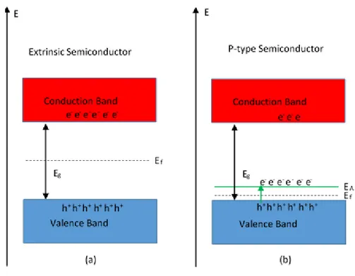
Figure 1.3 Band diagram of an (a) extrinsic and (b) p-type semiconductor.
eV and kT = 0.03 eV), 10-10 cm-3[9]. As a result of this the fermi level (Ef), being defined as the energy at which a 50 % chance of electron occupation occurs, is equal to
approximately Eg/2 for intrinsic semiconductors. The fermi level and therefore
conductivity (p-type or n-type) of a semiconductor can be modified by the addition of impurity dopants or defect energy states within the bandgap. Band diagrams of an intrinsic and p-type semiconductor are shown in Figure 1.3. Acceptor energy states (EA) are located near the valence band as seen in Figure 1.3(b) and are able to accept
6
electrons, making holes the majority carrier and shifts the fermi level between EA and the valence band. If the energy state is near the conduction band (donor - ED), it can be easily thermally ionized to donate extra electrons to the band and electrons become the majority charge carrier in the semiconductor (n-type conductivity).
A solar cell is essentially a p-n diode, consisting of a p-type semiconductor brought into metallurgical contact with an n-type region, and the bandgap of the
semiconductor is on the order of the solar spectrum, thus allowing for charge carriers to be generated. If the p-n junction is formed from a single semiconductor (e.g. p-type Si and n-type Si) it is a homojunction solar cell and is called a heterojunction if it is formed with two different materials (e.g. CdTe and CdS). When the n- and p-type regions are contacted, majority carrier electrons diffuse from the n-type to p-type and holes
correspondingly diffuse in the opposite direction[9]. As electrons and holes diffuse, fixed positively charged donor atoms on the n-type side and fixed negatively charged
Figure 1.4 Depletion region of a p-n junction[10].
acceptor atoms on the p-type side of the interface set up a net electric field that
opposes the direction of diffusion, seen as the yellow area in Figure 1.4. This diffusion occurs until a necessary width depleted of majority carriers at the p-n interface has been reached allowing for the electric field to balance the diffusion force[9].
7
It is this built in potential drop at the p-n junction that allows for photo generated electron-hole pairs to be separated (drift) and transported to electrical contacts to perform work through an external circuit. The electron-hole pairs are first generated by absorption of a photon that has an energy greater than or equal to the band gap. Transport of the pair to the built in potential for separation and contribution towards photocurrent depends on the rate of recombination of the electron-hole pair. The rate of recombination relies relates to minority carrier lifetime and diffusion length, with the mechanism for recombination either being band to band relaxations (radiative), deep level defect traps, or Auger recombination[11]. Once in the depletion region, the alignment of the fermi levels in the n- and p-type regions causes band bending of the
Figure 1.5 Band bending in a p-n junction[12].
conduction and valence bands over the depletion region, as illustrated in Figure 1.5. This band bending allows electrons to travel into the n-type material and for holes to go into the p-type under action of the built in voltage and this generates photocurrent.
8
The current-voltage characteristics of a solar cell under illumination can be modeled by an equivalent circuit containing a short circuit current source (Isc) in parallel with two diodes that oppose the flow of the current, shown in Figure 1.6, and includes shunt (RSh) resistor and series (RS) resistors. Diode 1 in Figure 1.6 constitutes
Figure 1.6. Equivalent circuit of a solar cell[13].
recombination in the bulk n- and p-type regions and diode 2 corresponds to recombination currents that occur in the depletion region. Rs is caused by the resistances of the semiconductor thin films and RSh is due to defects and current leakage across the pn junction. Total current from the solar cell (I) is therefore equal to the short circuit current (Isc) minus current lost in the two opposing diodes and resistors described by Equation 2-1.
� = �
�− � (
�+� �
�
− ) − � (
�+� ��− ) −
�− �9
Where I01 and I02 represent the dark saturation currents for the two opposing diodes, T is
the absolute temperature, V is the voltage across the cell, k is Boltzmann’s constant,
and q is the elementary charge.
A common plot of current density (J), obtained by dividing the current produced by the cell by the device area, against voltage yields the four central metrics for
comparing the performance of different solar cells: open circuit voltage (VOC), short circuit current density (JSC), fill factor (FF), and overall power conversion efficiency ( ). A diagram showing typical the typical J-V curve of a solar cell under standard illumination
Figure 1.7 J-V characteristics of a 13 % solar cell
conditions (AM 1.5) and characteristics for a 13 % power conversion efficiency are shown in Figure 1.7. When no external load is connected to the terminals solar cell, the resulting voltage is the Voc and corresponds to the x-intercept in the blue J-V curve in Figure 1.7. When the terminals of the cell are shorted, the resulting current is the Jsc.
10
The max power density (Pmp) of the device is found when the product JV is maximized and is found at Vmp and Jmp on the JV curve. The ideality of the device is calculated by:
�� =
��� (2-2)
This value is graphically seen as the ratio of the green rectangle to black one. The power conversion efficiency is the ultimate metric for comparing several cells because it accounts for all major characteristics of the J-V curve and is calculated by determine the ratio of the device maximum output power to the input device power.
=
���
% =
�� � �
��
%
(2-3)1.3 Solar Cell Technologies
Currently the main solar cell technologies that makeup the global solar module production are polycrystalline silicon (poly c-Si), monocrystalline silicon (mono c-Si),
11
amorphous silicon (a-Si), cadmium telluride (CdTe), and copper indium gallium selenide (Cu(InGa)Se2). The materials denote the absorber material in each solar cell technology and yield highly efficient power conversion efficiencies because of suitable allignment between their bandgaps and the terrestrial AM 1.5 solar spectrum as seen in Figure 1.8. The majority of photovoltaic manufacturing is in poly c-Si and mono c-Si with cumulative module productions for these technologies accounting for 91 % of the 48,961 MW market in 2014[6]. The next largest contributor is CdTe (4 %) followed by a-Si (3%) and CIGS (3%).
Crystalline silicon has dominated in photovoltaics mainly due to the already established Si wafer intrastructure that began in the 1960s, allowing the PV industry to cheaply and quickly adapt much of the already established Si research and technology to create photovoltaic devices. Despite the c-Si majority makeup of the market, a high cost of production for quality crystalline material and a low optical absorption coefficient pose serious drawbacks for the c-Si technologies that will eventually lead to a loosening of its hold on the market. The low optical absorption coefficient is a consequence of its indirect band gap, requiring c-Si cell thicknesses on the order of 100 µm for near complete absorption of the AM 1.5 photons. The charge carriers must exhibit high mobilities in c-Si in order to transport through the material, avoiding defects and
recombination sites, to the front and back contacts where power can be extracted. Low defect densities and high mobilities are obtained in Si that is crystalline thus requiring high processing temperatures[13].
12
The remainder of the major PV technoligies (CdTe, CIGS, a-Si) are direct bandgap materials giving high optical absorption coefficients that enable cells with thicknesses that are two orders of magnitude lower than c-Si for total absorption of AM 1.5 photons . A thinner cell reduces manufacturing costs because less overall material is consumed, and the required defect density is much less than c-Si due to charge carriers traveling shorter distances to the front and back contacts. Out of the thin film PV technologies, CdTe shows great potential to compete with Si as the leading PV material as evidenced by its lower levelized cost of electricity (LCOE) when compared to poly c-Si ($0.11/kWh < $0.14/kWh)[15] and steady increase in champion cell efficiencies (22.1 % in 2016 – First Solar). The CdTe photovoltaic device will remain the central topic for the remainder of the thesis.
1.4 Thin Film CdTe Solar Cells
Cadmium telluride is a II-VI binary compound with a bandgap of 1.45 eV with a thermodynamic potential efficiency of ~30 %. Its high optical absorption coefficient, 5 x 105 cm-1, allows for just 2 µm of material to absorb 99 % of the photons with energy greater than Eg = 1.45 eV in the AM 1.5 solar spectrum[13]. At typical processing temperatures (400 – 600 ºC) polycrstalline CdTe gives shallow level cadmium vacancy defects (VCd) causing p-type conductivity and are suitable to form a p-n heterojunction with n-type CdS (Eg = 2.4 eV)[14]. High efficiency solar cells are deposited in the
13 Figure 1.9 CdTe superstrate configuration[14].
superstrate configuration, shown in Figure 1.9, where the front contact/CdS/CdTe/back contact are deposited sequentially onto soda lime glass and light reaches the absorber by entering from the glass substrate.The front contact is a transparent conducting oxide and is either indium tin oxide (ITO), fluorine tin oxide (FTO), or cadmium stannate (CTO) for CdTe/CdS solar cells. TCOs must simultaneously have low sheet resistances and high transmittance in order to allow for photons to reach the absorber and for charge carriers to be extracted. As the thickness of the TCO increases, optical
transmission reduces and sheet resistance increases which corresponds to about 150 – 500 nm of thickness for CdTe applications if FTO is used. FTO films are usually
deposited onto glass substrates by atmospheric pressure chemical vapor deposition giving an optical bandgap of 3.80 eV, a resistivity less than 10-3Ω·cm, a transmittance of 83 %, and a carrier concentration of 1020 cm-3[16]. A highly resistive, transparent
14
oxide (HRT) layer is sometimes deposited between the TCO and CdS in order to decrease local shunting and increase junction quality by preventing TCO/CdTe junctions. Common materials for the HRT layer include SnO2[17] and ZnSnOx[18].
The CdS window layer is deposited onto the front contact serving as the n-type partner in the p-n heterojunction and is also a II-VI compound allowing for interdiffusion with CdTe, exhibiting hexagonal wurtzite or cubic zincblende structures (Figure 1.10) depending on the deposition technique and conditions. At higher annealing and
deposition temperatures, more of the hexagonal phase of CdS is found. CdS films are commonly deposited by chemical bath deposition (CBD)[21], thermal evaporation[22], metal organic chemical vapor deposition[23], and RF sputtering[24]. A carrier
Figure 1.10 Hexagonal wurtzite (a) and (b) cubic zincblende structures[19].
concentration of 1016 cm-3 is usually obtained in deposited films indicating that the depletion width exists almost entirely in the CdTe layer. Its wide 2.42 eV bandgap ensures that a significant portion of the AM 1.5 photons are not absorbed in the window and can be contribute to photocurrent after being absorbed in the CdTe layer. Some of
15
the photons with energies equal to or in excess of 2.42 eV can still pass through the window layer by depositing a very thin film of CdS, usually 80 – 200 nm. However, to overcome these losses groups have been developing high bandgap alternative to CdS such as CdS:O, CdxZn1-xS, and MgZnO.
In accordance with the superstrate architecture, the next thin film to be deposited is the CdTe absorber. A cubic zincblende structure is found for CdTe with a lattice constant of 0.6481 nm, giving a 10 % CdS/CdTe lattice mismatch. Figure 1.11 shows that the vapor pressures of Cd and Te2 are significantly greater than CdTe, ensuring that only single-phase, stoichiometric depositions are obtained. A congruent sublimation reaction occurs for CdTe that allows the partial pressure of Cd atoms to be twice the
Figure 1.11 Vapor pressure data for absorber and window layer components[13].
partial pressure of Te2 molecules, giving a vapor phase composition that matches the solid phase stoichiometry[13]. These properties allow for a number of robust
commercial manufacturing processes for photovoltaic grade CdTe films, all of which deposit 2-5 µm of polycrystalline material. Some of the common manufacturing
16
techniques include physical vapor deposition (PVD)[25], closed-space sublimation (CSS)[26], vapor transport deposition (VTD)[27], sputter deposition[28], and
electrodeposition[29]. CSS depositions occur by heating a CdTe containing graphite crucible to 650 – 750 ºC at ~1 Torr, causing the mass transfer the of source vapors to become diffusion limited. As a result of this the substrate, independently heat at ~600 ºC, must be brought within several millimeters of the source for 1-5 µm/min deposition rates to occur[13]. The deposition occurs in an inert gas with a small oxygen partial pressure. VTD occurs by convective mass transfer of CdTe onto a substrate from a saturated inert carrier gas as seen in Figure 1.12. Similar to CSS, the substrate temperature is independently controlled from the source in VTD but a carrier gas is introduced at the source which becomes saturated with vapors which then condenses into a film at the substrate when the stream becomes supersaturated. Because
convective mass transfer occurs and a moving substrate can be introduce, very large deposition rates occur and this technique is currently the main deposition technique for commercial manufacturing.
After deposition of the absorber, an anneal in a chlorine containing environment, known as the cadmium chloride (CdCl2) treatment or activation, must be performed on the as-deposited CdS/CdTe stack in order for the solar cell to generate reasonable photocurrents and voltages. The performance usually increases by almost an order of magnitude when compared to devices that are not activated. Much of the CdTe
research is still focused on this processing step, aiming at an understanding of what conditions lead to material properties that give quality photovoltaic devices[30]. Post-treated devices show intergranular and intragranular recrystallization, grain growth,
17
interdiffusion at the CdTe/CdS junction, and grain boundary passivation in the absorber layer[31-34]. Higher photocurrents and voltages are obtained because a reduction in recombination centers and defect densities along with increased p-type conductivity, a graded bandgap structure, and removal of lattice mismatch.
Activation treatments are either performed by a solution or vapor-phase processing. Solution treatments begin by dissolving CdCl2 in methanol or deionized water followed by application achieved by dipping the substrate into the solution or spraying the solution on the substrate. The samples are then activated by heating to ~400 ºC for 10 – 30 min in air or a N2/O2 mixture. Vapor-phase processing consists of bringing the substrate surface to close proximity of solid CdCl2 and heating the source to ~400 ºC, causing the vapors do diffuse into the substrate. The conditions employed are similar to solution processing. The presence of O2 in the anneal has been found to be crucial for improvements in fill factor and open-circuit voltage.
After the CdCl2 activation, the final step in fabrication of CdTe solar cells is to deposit ohmic back contacts onto the CdTe layer in order for electrical current to be efficiently extracted. Ohmic contacts are difficult to with CdTe because it is a high-resistivity p-type semiconductor with a high work function (5.9 eV) causing metals, which have considerably lower work functions, to form Schottky barriers. Schottky barriers are undesirable because they are rectifying, allowing current to flow in one direction, and in CdTe the Schottky diode opposes the p-n junction diode, causing limitations in hole transport[35]. Low-resistance ohmic back contacts are formed on CdTe by depositing an interfacial semiconductor layer with properties such as negligible CdTe valence band discontinuity, lower work function, and having an ability for p-type
18
doping to induce tunneling effects. Common materials used for this method are CuxTe (1 < x < 2)[36] and ZnTe:Cu [37]. For CuxTe depositions, a chemical etch is used to create Te excess on the CdTe surface which then reacts with a deposited Cu film to form the buffer layer. Depositions of ZnTe:Cu films occurs by either sputtering [38] or co-evaporation of Cu and ZnTe onto a chemically etched CdTe surface followed by thermal anneals to optimize the Cu profile. After deposition of the interfacial buffer layer the metal contact is deposited by physical vapor deposition. Gold is often used in
laboratories due to its high work function, but numerous other metals have been used including nickel, chromium and titanium.
1.5 CdTe Activation
The focus this thesis was to develop molecular chlorine (Cl2) as an alternative activation treatment to CdCl2 activation. In this section a brief review of the literature on CdCl2 activation is presented. Challenges of this conventional treatment is discussed along with a review of the results from alternative treatments. Finally, the potential benefits of a gaseous Cl2 activation are highlighted and the goals of this thesis are enumerated.
Although specific effects due to an activation are primarily a function of the thermochemical history of previously deposited layers, there are common structural, chemical, and optoelectronic properties that are reported when a treatment is properly optimized. Structural and morphological changes usually occur by differences in grain orientation, size, extent of recrystallization, and defect densities to varying intensities after the activation. Intragranular and/or intergranular recrystallization occurs after the
19
performing the treatment. Intragranular recrystallization almost always occurs,
regardless of the exact treatment method and previous deposition methods, causing the orientation of the grains to become more randomized. The extent of intragranular
recrystallization is measured with x-ray diffraction. It is generally observed by tracking the change in orientation of the thin film CdTe grains from along the <111> direction (normal to substrate) to becoming randomly distributed. In other words, if the film significantly loses texture in the (111) plane during the CdCl2 activation then recrystallization within each grain must have occurred. Grain coalescence or
intergranular recrystallization is observed when the grains increase in mean diameter. Intragranular recrystallization almost always occurs but intergranular does not.
Intergranular recrystallization does not occur in CSS or VTD films deposited at high substrate temperatures because the surface energy is pinned before treatment,
resulting in large as-deposited grain sizes that do not change significantly in size during activation. Thermal evaporation and sputtering, for example, often employ low
temperatures and pressures during deposition which result in small grains in the as-deposited films, indicating that the surface energy has not been pinned yet. After the activation treatment, the thermally evaporated and sputtered films will show grain enlargement.
Recrystallization results in a relaxation of lattice strain, driven by an initial high density of stacking faults with, again, a more drastic change observed for CdTe films grown at low substrate temperatures. Interdiffusion at the CdS/CdTe also occurs by S diffusion into the CdTe layer and Te diffusion into the CdS layer resulting in CdTe1-xSx and CdS1-yTey alloys, respectively. There are both benefits and drawbacks associated
20
with this process. CdTe1-xSx formation results in a lower bandgap in the absorber layer due an optical bowing effect in the ternary alloy and causes a beneficial higher long wave photon conversions. The CdS1-yTey layer gives a lower bandgap in the window layer due to the optical bowing effect, reducing short wave photon conversions for the device. Another major benefit is that the 10 % lattice mismatch at the CdS/CdTe is significantly reduced and a grading effect in the bandgap can be seen. This results in a decrease in strain and defect densities at the interface. Because the CdS window layer initially very thin compared to the absorber, the interdiffusion can result in complete consumption of the CdS layer causing a reduction in Voc. Shorter CdCl2 have been used on the as-deposited CdS layer in order to prevent subsequent interdiffusion during the CdTe activation [39]. The addition of a separate CdS activation is time consuming so the extent of diffusion is generally controlled and optimized to obtain a maximum device efficiency by varying the CdTe treatment temperature, time, and oxygen partial
pressure.
Suitable electronic structures of CdTe for quality heterojunction formation are due to the stabilization of high p-type conductivity, caused by shallow level complexes (Tei2—ClTe+)- and or (VCd2—ClTe+)- [40]. Although the enhanced p-type conductivity is important for form a quality heterojunction, the defect complexes are non-uniform throughout the activated CdTe and causes a reduction in Voc [41]. Excess of CdCl2 can also lead to oxychloride precipitates in the CdTe layer and at the junction which causes a detriment to device performance most likely due to insulating effects
Although the CdCl2 treatment is paramount to the CdTe device fabrication sequence, there are numerous drawbacks associated with this process that limit
21
economic, safety, and processing prospects. Although cadmium is found throughout many layers of the solar cell, these sources do not pose significant environmental risks because these compounds are not water soluble (e.g. CdTe and CdS). CdCl2 is highly soluble in water and is the main source for cadmium emission during device production. Because a high risk of cadmium emission is associated with CdCl2, special
infrastructure is required to process and store the material, and this causes the activation treatment to be capex intensive. Treatment times can be as long as 1 hr, significantly adding to the overall manufacturing time for solar cell production, which is highly undesirable because the entire fabrication sequence is inherently a batch
process. CdCl2 is a hygroscopic salt that requires periodic removal of the material from annealing furnaces for drying or replacement. Optimization of treatments are quite intricate and easily thrown out of order because the vapor-solid equilibrium couples the concentration and temperature of the CdCl2 molecules. This causes run-to-run control and reproducibility issues in the quality of obtained solar cells from the activation step, which again can be expensive and time consuming.
As a result of the many drawbacks associated with CdCl2 activations, several cadmium-free chlorides, vapors, and gasses have been studied as direct replacements for the activation process. A thermal treatment using a in dry difluorochloromethane (HCF2Cl) has been investigated in the literature as a gaseous activation treatment[42, 43, 44]. Salavei et al. used atomic force microscopy (AFM) to determine that a slightly higher temperature (420 ºC) was needed for the HCF2Cl treatment to obtain similar grain sizes (2 µm) and recrystallization when compared to CdCl2 devices treated at
22
lower temperatures (410 ºC), seen in Figure 1.12. This treatment consisted of 10 mbar of HCF2Cl in 500 mbar of Ar for 5 - 20 min.
(a) (b)
Figure 1.12 AFM images of CdTe treated with (a) HCF2Cl at 420 ºC and (b) CdCl2 at 410 ºC showing similar 2 µm diameter grains. The CdCl2 has been etched[44].
Salavei et al. also showed that increasing the concentration from 10 mbar of HCF2Cl diluted in 50 mbar of Ar to 10 mbar of pure HCF2Cl resulted in less recrystallization as seen in Figure 1.13. This trend is somewhat counterintuitive.
23
A partial pressure of 50 mbar HCF2Cl in 400 mbar Ar, a time of 5 min, a temperature of 400 ºC, and no oxygen gave Vaillant et al. a 14.8 % efficient device with Voc = 820 mV, FF = 69 %, and Jsc = 26.2 mA cm-2. Interestingly, Rios-Flores et al. required oxygen during the treatment similar to a conventional CdCl2 activation to obtain an optimized 14 % efficient device with Voc = 828 mV, FF = 69 %, and Jsc = 26.2 mA cm-2. Other than the oxygen content the conditions were similar: 50 mbar HCF2Cl in 400 – 800 mbar of a O2/Ar mix, 400 ºC, and 5 min. It is possible that oxygen was needed during the
treatment because CdS was deposited in pure Ar while Vaillant et al. deposited CdS in a 90 % Ar and 10 % CHF3 ambient. The CHF3 may have limited CdS consumption during the activation step, which is a common role of oxygen and therefore did not require any presence of oxygen for optimization. Although quality devices have been obtained with a HCF2Cl treatment, this method is still undesirable because HCF2Cl is linked to ozone depletion and its usage is restricted.
Another studied alternative to CdCl2 is using HCl vapor or dry gas [45]. Qu et al. initially investigated HCl vapor treatments by bubbling Ar through a 25 Mol % solution but decided to switch to dry HCl gas diluted in Ar after equipment failure due to HCl vapor exposure. Grain growth was observed by SEM images when the HCl/Ar
concentration was increased from 0 – 5 % during a 30 min activation at 400 ºC and also when the temperature increased from 380 – 440 ºC. The (111) texture coefficient
decreased an as-deposited TC111 = 4-7 to TC111 = 1.2 when the HCl concentration was increased from 0 -5 %. These microstructural and morphological changes indicate that HCl can be an effective fluxing agent, similar to CdCl2. Using a HCl concentration of 5 %, a treatment temperature of 400 C, and a time of 30 min resulted in ~ 8 % devices.
24
Non-cadmium containing salts have also been investigated for CdCl2 alternatives and include MgCl2, NH4Cl, NaCl, HCl, KCl, and MnCl2[46, 47]. The performance results for these alternatives are shown in Table 1.1 and indicate that MgCl2 and NH4Cl can be used as replacements for a solid-vapor activation treatment. These electrical properties were correlated strongly with microstructural changes quantified by texture coefficients. The greatest extent of recrystallization resulted in the best efficiency, which was the case for the CdCl2 treatment. As seen in Table 1.2, the ranking in efficacy of each alternative is correlated with a reduction in TC(111). These results are important because they show that in order for an activation alternative to be successful, significant recrystallization must occur as indicated by a reduction in
Table 1.1 Performance results for device activated with non-cadmium containing salts[47].
Table 1.1 Performance results for device activated with non-cadmium containing salts[47].
25
Table 1.2. Texture coefficients for various activation salts at optimal conditions [48].
TC(111). If TC(111) does not approach a value of 1 after activation, significant strain the p-n interface, defect densities, etc. degrade performance of devices. Bond dissociation energies also correlate to efficiencies between salts because a lower bond energy allows for greater Cl dissociation and greater recrystallization (3 - 4 eV for CdCl2, MgCl2, and NH4Cl with > 4 eV for NaCl). Although these alternatives are non-toxic and produce devices that are comparable to the CdCl2 activation, they are solid materials that have solid-vapor equilibrium which necessarily couples concentration and temperature during processing. As previously discussed, this property causes run-to-run variation and makes control difficult during activation.
The common element between the above mentioned alternatives is Cl, which has led to one group reporting on the use of Cl2 gas as an activation agent [48]. In their report little information is given on the experimental conditions or film properties, but 9 – 10 % devices were obtained with exposure to a Cl2/N2 flow. Cl2 is particularly
encouraging because it does not contain cadmium, allows for precise gas phase delivery of Cl, and is an inexpensive source that is commercially available at a wide
26
range of concentrations at high purities. It is the scope of this thesis to explore the parameter space of an alternative activation treatment using molecular chlorine using microstructural and electrical characterization techniques. Goals for the activation treatment will be to determine if cadmium is required for highest efficiency devices, determine the most efficient conditions, and evaluate device performances. Additionally, the microstructural, morphological, electrical, and optoelectronic properties of a Cl2 activated device will be compared with a CdCl2 standard.
27 CHAPTER 2
EXPERIMENTAL METHODS
The information contained in Chapter 2 primarily consists of the experimental methods that were used throughout the course of research used in this thesis. It provides information on device fabrication and characterization conditions.
2.1 Substrate Preparation
Fabrication of superstrate CdTe devices began with proper cleaning of a TEC 15 (TCO/glass) substrate. TCO/glass substrates are generally characterized by the sheet resistance and visible light transmittance of the TCO layer, and for TEC 15 the TCO layer is ~200 nm of fluorine-doped tin oxide, giving a sheet resistance of <15 Ω/sq. and ~82 % light transmittance. Commercially available TEC 15 glass, at a thickness of 3.2
Figure 2.1 Schematic diagram of TEC 15 glass
mm, was cut into 1.η” x 1.η” squares with sample identification marks made via a precision diamond scribe. After cutting the glass, the surface of the TEC 15 substrates were cleaned by scrubbing both the FTO coated and glass surfaces with an alkaline cleaning concentrate (Micro-90®) soaked Kimwipe® for ~30 s followed by rinsing with
28
deionized water. After the deionized water rinse, it was found that blow drying first the glass side followed by the TCO side of the substrates resulted in less water droplet residue on TCO side, and a more uniform window layer could be deposited. The final step in the substrate cleaning process consisted of a 25 min exposure in an UV/ozone cleaner. The time between UV/ozone exposure of TEC 15 substrates and subsequent window layer deposition was always minimized at around 5-20 min, and it never exceeded more than 1 hour.
2.2 CdS Thermal Evaporation
After proper cleaning of FTO substrates, a 150 nm window layer of CdS was deposited onto the TCO in a thermal evaporator, shown in Figure 2.2. A diagram of the pumping and valve configurations of the system is given in Figure 2.3. The CdS source
Figure 2.2 Glass/FTO/CdS stack
consisted of 99.999 % pure chunks contained in a tungsten boat. The thermal
evaporator was equipped with a resistive substrate heater and a quartz crystal monitor (QCM), as seen in Figure 2.3, for control of the thickness and deposition rate of CdS films. The standard deposition consisted of pumping down the chamber to high vacuum (10-6 Torr) with a diffusion pump, backed by a rotary vane pump. A hot cathode
29
ionization gauge was used to measure high vacuum pressures, and a cold trap located at the inlet of the diffusion was filled with liquid nitrogen to obtain lower base pressures. Prior to connecting the diffusion pump to the chamber, the mechanical pump roughed the diffusion pump foreline and chamber to a base pressure of ~50 mTorr. Once a standard 150 ºC substrate temperature and HV was obtained in the chamber, approximately 60 amp of current was passed through the CdS containing crucible resulting in a ~5 Å/s deposition rate as measured by the QCM controller. The QCM was previously calibrated by depositing films and measuring thickness with contact
profilometry. The shutter was opened after the desirable deposition rate was obtained
for a total thickness of 1η0 nm. Up to four 1.η” x 1.η” substrates could be processed in the thermal evaporator per run, resulting in very uniform, transparent films. After removing the films from the substrate holder, no other cleaning techniques were performed before absorber deposition. Time was always minimized between CdS and absorber depositions with a maximum amount of elapsed time between depositions consisting of 4 hours.
2.3 CdTe Vapor Transport Deposition
After deposition of 150 nm of CdS a 3 – 4 µm thin film of CdTe was deposited by vapor transport deposition (VTD) at a substrate temperature of 420 ºC, 20 Torr nitrogen carrier gas, and 10? % oxygen (Figure 2.4). A real image and accompanying schematic
diagram of the system are given in Figures 2.5 and 2.6, respectively, on the following pages. Differential heating is employed in the quartz source tube to vaporize solid CdTe
30 Figure 2.3 Thermal evaporator diagram
31
into a flowing stream of nitrogen and to ensure that only saturated Cd and Te2 vapor pass through the porous frit.
Figure 2.4 Glass/FTO/CdS/CdTe stack
This is accomplished by maintaining a temperature difference of at least 15 ºC between the source and frit radiative heaters. Typical operating temperatures were 650 ºC for the source and 670 ºC for the frit. A 1.η” x 1.η” substrate holder was spaced ~0.75” below the quartz frit, which was always heated to 420 ºC with a SiC heating element. A shutter between the frit and substrate holder was used to control deposition, and a convection gauge monitored pressure at the CdTe source. Nitrogen was delivered to the inlet of the source tube with an electronic mass flow controller at a rate of 375 sccm. Oxygen was delivered at the bottom of the deposition chamber at a tenth of the nitrogen flow (37.5 sccm). Small amounts of oxygen was found to be crucial to depositions because of advantageous material properties of deposited CdTe films in an oxygen ambient and because the NiCr alloy heaters of the source and frit would form a native oxide in the
32
presence of oxygen during the high operating temperatures, preventing fracture/failure of the heating wires during depositions.
A standard deposition consisted of pumping down the deposition chamber with a mechanical pump to ~360 mTorr and setting the temperature controller to 420 ºC for the SiC heating element located beneath the substrate holder. After approximately 30 min, the substrate would nearly reach its setpoint, and the temperature controllers for the source and frit would be set to ~650 ºC and ~670 ºC, respectively. Immediately following the switching of the source and frit temperature controllers, nitrogen and oxygen gas flow was introduced to the chamber, and a resulting base pressure of 20 Torr was measured without the use of throttling/conductance valves. Once the source, frit, and substrate heaters reached setpoints, the shutters were opened and a 3 – 4 µm deposition was performed. Deposition rates were calibrated using contact profilometry with rates better than 0.78 µm/min obtained. Although the 420 ºC substrate temperature was never changed, the source and frit temperature would gradually be increased in order to maintain the ~1 µm/min deposition rates. The maximum source temperature used was 675 ºC after approximated 50 depositions. At this point the source tube would need to cleaned with nitric acid and the CdTe source chunks replenished.
2.4 Chlorine Activation
Following the vapor transport deposition of CdTe, the as-deposited stacks were recrystallized by gaseous chlorine (Cl2) activation. For comparisons and analysis, samples were also activated by the standard CdCl2 treatment. The standard CdCl2
33 Figure 2.5 VTD System Image
34 Figure 2.6 VTD Schematic Diagram
35
1.η” samples placed in a graphite holder that contained CdCl2 chunks. Typical processing began by purging the quartz tube at atmospheric pressure in a 50/50 oxygen and nitrogen mixture at 2000 sccm for 20 min. After 20 min, the heaters were powered and the flow was reduced to 400 sccm while maintaining the 50/50 oxygen and nitrogen composition. Once the thermocouple positioned above the graphite crucible reached 400 ºC, 30 min would be allowed to elapse before the power to the heaters was switched off. The 400 sccm gas mixture would continue to flow until the furnace reached 290 ºC, at which point the samples were completely removed from the quartz tube and quickly cooled under ambient conditions to room temperature.
For the novel activation of the as-deposited glass/FTO/CdS/CdTe with gaseous Cl2, a custom tube furnace was designed constructed and is schematically shown on the following page in Figure 2.7. All piping was constructed of 1/4” 31θL stainless steel and the material construction of the tube was quartz. Table 2.1 indicates the specifications of the quartz tube which was enclosed by ceramic heating material. Mass flow controllers
Table 2.1 Quartz tube specifications.
(MFC) used to independently control flow of nitrogen, oxygen, and 3 % Cl2/Ar to the furnace with maximum flow rates of 833 sccm, 300 sccm and 5 sccm, respectively. The 3 % Cl2/Ar cylinder was equipped with a reactive gas regulator allowing for it to be either purged with another line of pure Ar or to be pumped down to rough vacuum with a
Material Diameter (mm)Outer Wall Thickness (mm) Length (mm) Notes Company
36 Figure 2.7 Cl2 Tube Furnace
37
with a mechanical pump. The regular essentially was a four way valve allowing all possible connections between a pure Ar inlet, a 3 % Cl2/Ar inlet, a rough vacuum, and a line to a furnace MFC. A thermocouple was inserted directly in the middle of the quartz tube. A needle valve downstream of the furnace allowed for modulation of conductance and was always adjusted until a system pressure of 600 Torr was found during full gas flow. After a substrate was loaded into the middle of the furnace, the tube was pumped down to ~100 mTorr with a mechanical pump followed by delivery of a set
nitrogen/oxygen composition via the MFCs. Regardless of the composition of O2/N2 mixture, the total flow rate was always set to 800 sccm, and the initial base pressure before gas introduction was read with a 10 Torr capacitance manometer, seen as P1 in Figure 2.7. During this time the Cl2 MFC connected to only pure Ar via the reactive gas regulator and was set to a desired flow rate. After initiating gas flow, the throttling valve was adjusted until a pressure of 600 Torr was read on a 1000 Torr capacitance
manometer, as denoted by P2 in Figure 2.7, and the temperature controller was set to around 400 ºC. Once the temperature setpoint was reached, the pure Ar to the Cl2 MFC and the valve in front of the MFC were closed. The vacuum line between the reactive gas regular and the mechanical pump was next opened, allowing for the line between the outlet of the Cl2 MFC and the outlet of the 3 % Cl2/Ar to be pumped down to rough vacuum. Once this was achieved, the vacuum line was closed off and the outlet of the 3 % Cl2/Ar was opened. A timer was started after opening the valve in front of the Cl2, constituting a t = 0 reaction time. After the reaction, the valve in front of the Cl2 was closed and power to the heater was cut. The Cl2 line was pumped down to rough vacuum with pure Ar being subsequently supplied to purge the reactive gas regulator
38
and any residual Cl2 in the system. During cool down, the O2/N2 mixture at 600 Torr was allowed to keep flowing in addition to pure Ar through the Cl2 MFC. At approximately 150 ºC, the substrate was removed from the quartz tube and cooled in ambient
conditions. Table 2.2 summarizes the various conditions of the tube furnace that were studied throughout the duration of the research.
Table 2.2 Studied conditions of Cl2 tube furnace
2.5 ZnTe:Cu Contacts
After the Cl2 or CdCl2 activation step, a cleaning procedure occurs where the sample is completely immersed in a 0.05 % Br2/methanol (200 mL MeOH + 0.1 mL Br2) solution under gentle agitation for 10 sec followed by a pure MeOH rinse. Elemental halogens and their solutions etch II-VI compounds, and as a result, this cleaning removes oxide precipitates and causing Te excess, yielding an increased p-type conductivity at the exposed surface of the CdTe layer which is important for creating ohmic contacts.
Once the substrates are removed from the MeOH rinse, the samples were
allowed to air dry for ~10 min before being placed in a thermal evaporator for deposition of a 150 nm film of ZnTe:Cu onto the 3-4 µm of CdTe, as shown in Figure 2.8(a). The deposition occurred in the same system as one used for CdS deposition but another set
Temperature (°C)
3 % Cl2/Ar Flowrate (sccm)
O2/N2
Composition (%) Time (min) Pressure (Torr)
39
Figure 2.8 Schematic of completed devices (a) and corresponding image of completed devices (b)
of electrodes was employed in order to perform co-evaporation from 99.999 % pure Cu in one set and 99.999 % pure ZnTe in another. A baffle was placed between the two sets of electrodes allowing for two QCMs to measure and independently control
deposition rate of pure Cu and ZnTe (Figure 2.9). The substrate temperature was set to 100 ºC and a 10-6 Torr high vacuum was used, similar to the CdS depositions. Because ZnTe has a significantly lower pressure, the maximum deposition rate as measured by the QCM was always obtained with the Cu deposition rate being accordingly set to 10 % of this value. A typical maximum deposition rate for ZnTe was ~1.5 Å/s at ~50 amp, thus the typical Cu deposition rate was 0.1 Å/s at ~80 amp. Regardless of deposition rates,
40
Figure 2.9 Addition of a baffle for thermal co-evaporation.
the shutter was closed when ZnTe and Cu films grew to 150 nm and 10 nm,
respectively. Immediately following the closing of the shutter, the power to the two sets of electrodes and substrate heater was removed. 100 nm metallization layers of Au pads were subsequently evaporated in the same system onto the ZnTe:Cu film using a shadow mask and are schematically shown in Figure 2.8(a). Each Au pad had an area of 0.079 cm2 and defined the area for each device on the ZnTe:Cu film. The standard Au deposition rate was ~5 Å/s at ~80 amperes. Following the deposition of Au pads, a diamond tipped scribe was used to scribe around each gold dot down to the FTO, resulting in electrically isolated 0.079 cm2 devices. A razor was used to remove material
around the edges of the 1.η” x 1.η” sample down to the FTO after which indium was applied to the exposed front contact with a soldering gun, shown schematically in Figure 2.8(a) and as a real image in Figure 2.8(b).
41
Following the application of indium to the front contact and scribing devices, rapid thermal processing (RTP) was employed to activate the back contact by optimizing the diffusion of Cu into the ZnTe and CdTe layers. The RTP system consists of a ceramic substrate holder, radiative heaters, injection of Ar gas, and a mechanical pump. Images of the system are shown in Figure 2.10. The standard process began by pumping down the volume to rough vacuum followed by Ar delivery at ~30 Torr. Once a stable flow rate was obtained, the temperature trajectory was programmed. Every sample
underwent a standard room temperature to 320 ºC ramp in 20 s followed by a 30 s dwell at 320 ºC. Once the system was at 200 ºC, another 20 s ramp and 30 s dwell at 330 ºC was programmed. After the sample cooled to 200 ºC under 30 Torr of Ar flow, the sample was removed and cool to room temperature. The RTP treatment is the final
Figure 2.10 Rapid Thermal Processing (RTP)
processing step in the fabrication of CdTe solar cells and allows for probes to be connected to the front and back contacts for electrical measurements.
42 2.6 X-Ray Diffraction
X-ray diffraction (XRD) a powerful, non-destructive technique that gives phase and microstructural information of thin films by measuring properties such as grain size, lattice spacing, lattice strain, dislocation density, alloying, film texture, crystallinity, surface structure, etc. Diffraction of X-rays occurs when the wavelength of the incident electromagnetic waves becomes comparable to the interatomic distances that are perpendicular to the thin film surface, resulting in the constructive interference of the
waves at angles specified by Bragg’s law:
� =
ℎsin
(2.1)where λ is the wavelength (Å) of the radiation, dhkl is spacing (Å) of a family of parallel (hkl) atomic planes, and (degrees) is the angle of incidence of the X-ray. Bragg’s law can be derived from basic geometry as seen in Figure 2.11:
43
X-ray diffractometers generally consist of an X-ray source, incidental angle optics, a goniometer, and detection optics, resulting in a plot of intensity vs.. Analysis of the resulting peak intensities, Bragg angle location, full width at half maximums, d-space, and integrated areas provides insight into the above mentioned properties of thin films. A copper anode was used as a source for scans of all samples using Cu Kα radiation at
λ = 1.54 Å. Wide angle scans in the 2 range of 20 - 80º were taken for all samples that underwent texture coefficient analysis with an increment of 0.05º at a dwell time of 1 sec.
As previously mentioned, the texture coefficient is a measure of the orientation of grains and extent of recrystallization in polycrystalline CdTe films. The texture
coefficient was used as an indicator of how much recrystallization took place when variables such as oxygen concentration, chlorine concentration, temperature, and time were varied and these values were compared against the extent of recrystallization of a standard CdCl2 activated sample for insight. To start off the texture coefficient analysis, a 20 - 80º/0.05/1sec 2 was taken, as shown in Figure 2.12 on an activated
glass/FTO/CdS/CdTe stack after a 10 s Br/MeOH etch. Only the 7 planes allowed for cubic zincblende CdTe in this 2 range are indexed and used during the texture coefficient analysis of samples. All other planes, due to oxides and TCO, show low intensities and are neglected in the CdTe texture coefficient analysis. The intensities are normalized by the (111) plane in Figure 2.12 for clarity, but it is the measured intensities (height) which are used during the analysis. After each scan, software was used to subtract the background by fitting a cubic spline function and the Cu Kα2 doublets were
44
Figure 2.12 Standard 20 – 80º XRD scans of activated samples
Table 2.3 Post-processed XRD data suitable for TC analysis
2-Theta d(Å) Height H% Area A% FWHM
1.5 SCCM 3% Cl2/Ar 23.694 3.752 1822 57.6 343.6 59.1 0.16 39.208 2.2959 3162 100 581.5 100 0.156 46.347 1.9575 1789 56.6 309.2 53.2 0.147 56.664 1.6231 290 9.2 45.5 7.8 0.134 62.317 1.4888 628 19.9 117.1 20.1 0.158 71.141 1.3242 541 17.1 99 17 0.155 76.177 1.2487 179 5.7 33.1 5.7 0.157 CdCl2 Activated 23.581 3.7698 4071 100 752.9 100 0.157 39.095 2.3022 3849 94.6 650.6 86.4 0.144 46.24 1.9618 2379 58.4 415.4 55.2 0.148 56.553 1.626 1154 28.4 198.2 26.3 0.146 62.216 1.4909 561 13.8 106.2 14.1 0.161 71.042 1.3258 519 12.8 94.6 12.6 0.155 76.061 1.2503 457 11.2 92.2 12.2 0.171
45
removed. The software also used statistical methods to fit each peak and determine the Bragg angle location, height, FWHM, and area. An example final, post-processed data that is suitable for texture coefficient analysis is given in Table 2.3. The texture
coefficient (TC) was calculated according to the following equation:
��
=
�∑
7 ℎℎ�=
−
(2.2)
where TC(111) gives the TC of the (111) plane for the polycrystalline film, I(111) is the as-measured intensity for the (111) plane, I0(111) is the reported (111) intensity from a standard powder diffraction file (PDF). In the denominator of the expression, a
summation of the measured intensity I(hkl) normalized by the corresponding PDF intensity I0(hkl) is performed over the remaining observed Bragg planes in the 2 scan for a particular phase, where n is the total number of observed Bragg planes used in the calculation. The variable n is always equal to 7 for the presented TC analyses. As a result of a few mathematical constraints, several useful conclusions can be drawn from the value of the (111) texture coefficient. If the all of the grains are oriented along the (111) plane the only measured intensity is from (111), and TC(111) = 7 because the denominator becomes 1/7*[I(111)/I0(111) + 0 + 0 + 0 + 0 + 0 + 0 ] = 1/7*[I(111)/7I0(111)] and the numerator becomes I(111)/I0(111). A value of TC(111) = 7 after a Cl2 indicates that no recrystallization took place during the treatment because as-deposited films generally give TC(111) = 7. If TC(111) = 1, the grains in the film have become perfectly randomly oriented because all (hkl) planes have intensities equal to their PDF values. Thus, in the range 1 < TC(111) < 7 a relative measurement of the extent of
46
recrystallization between samples can be determined. If TC(111) < 1, the film has some degree of preferential orientation along another (hkl) plane.
2.7 Solar Simulator
The basic equations and operating principles of a solar simulator were outlined in the introduction, and the basic equipment used for testing of fabricated cells was
obtained from a commercially available solar simulator. The system was fully automated and tested cells under standard AM 1.5 illumination. A basic circuit of a general solar simulator consists of a DC voltage source, AM 1.5 source, an oscilloscope, a
programmable multimeter, and a computer equipped with a control software. Essentially, the multimeter measures the voltage drop across the solar cell and the amount of current for a given applied DC voltage while under AM 1.5 illumination. The computer performs automated electrical and calibration calculations resulting in a characteristic I-V curve per “flash” of AM 1.η illumination. Two wires constitute probes with one connected to the front contact and the other to the back contact. On the commercial system, a reverse to forward sweep direction was performed in the voltage range of -2 to 1 V at a source irradiance of 100 mW/cm2. As part of the automation, the Voc, Jsc, FF, and would automatically be tabulated in addition to the characteristic J-V curve.
47 CHAPTER 3 Results and Discussion
This chapter represents the majority of results obtained throughout the duration of the research and has been adapted from work that is currently in preparation for submission to the 43rd IEEE Photovoltaic Specialists Conference, Portland, OR 2016.
3.1 Activation of CdTe Solar Cells Using Molecular Chlorine
Abstract — There has been renewed interest in developing alternatives to CdCl2 activation, a critical but expensive step in CdTe manufacturing. A common element among the alternative agents that have been explored is chlorine, which facilitates recrystallization, passivates grain boundaries, and leads to enhanced efficiency. In this paper we present an evaluation of molecular chlorine (Cl2) for CdTe activation. The broad process space was first screened by evaluating the change in the (111) texture coefficient. It is shown that recrystallization occurs quite quickly (~1
minute), and the required concentration of Cl2 is quite low (<100 ppm). Devices fabricated at promising conditions displayed good rectification with device efficiency greater than 11%.
3.2 Introduction
A critical step in CdTe solar cell production is its activation through exposure to CdCl2. This process results in recrystallization, grain growth, and interdiffusion with the CdS window layer [31, 32]. It has been shown that during this process Cl rapidly diffuses

![Figure 1.5 Band bending in a p-n junction[12].](https://thumb-eu.123doks.com/thumbv2/5dokorg/4332221.98177/19.918.217.713.525.811/figure-band-bending-p-n-junction.webp)
![Figure 1.6. Equivalent circuit of a solar cell[13].](https://thumb-eu.123doks.com/thumbv2/5dokorg/4332221.98177/20.918.229.667.277.495/figure-equivalent-circuit-of-a-solar-cell.webp)

![Figure 1.8 Solar cell efficiency as a function bandgap for terrestial illumination[14]](https://thumb-eu.123doks.com/thumbv2/5dokorg/4332221.98177/22.918.278.643.703.997/figure-solar-cell-efficiency-function-bandgap-terrestial-illumination.webp)

![Table 1.1 Performance results for device activated with non-cadmium containing salts[47]](https://thumb-eu.123doks.com/thumbv2/5dokorg/4332221.98177/36.918.193.742.673.933/table-performance-results-device-activated-cadmium-containing-salts.webp)
![Table 1.2. Texture coefficients for various activation salts at optimal conditions [48]](https://thumb-eu.123doks.com/thumbv2/5dokorg/4332221.98177/37.918.184.734.154.396/table-texture-coefficients-various-activation-salts-optimal-conditions.webp)

