Department of Physics
Ume˚
a University, Sweden
Master’s Thesis in Physics
Fabrication of surface enhanced Raman spectroscopy
(SERS) active substrates based on vertically aligned
nitrogen doped carbon nanotube forest
Author:
Md Khorshed Alam
Email:
mdal0015@gapps.umu.se
Supervisor:
Xueen Jia
Examiner: Thomas W˚
agberg
Acknowledgements
Thomas W˚agberg, Xueen Jia, Roushdey Salh, Tiva Sharifi, Joakim Ekspong,
Cheng Choo Lee, Gabriella Allansson, Roger Halling, Michael Bradley, Jens
Zamanian, Guangzhi Hu, Shibbir Ahmed, Robin Sandstr¨om, Nicolas Boulanger,
Contents
1 Introduction . . . 1
1.1 Photolithography . . . 2
1.2 Chemical vapor deposition (CVD) . . . 3
1.3 Physical vapor deposition (PVD) . . . 6
1.4 Scanning Electron Microscope (SEM) . . . 8
1.5 Surface Enhanced Raman Spectroscopy (SERS) . . . . 9
1.6 Enhancement Factor of a SERS system . . . 11
2 Experimental setup and procedure . . . 12
3 Results . . . 18
3.1 Vertically aligned N-doped CNT forest growth onto the substrates . . . 18
3.2 N-doped CNT forest characterization through the SEM imaging . . . 20
3.3 SEM image characterization after evaporation of the Ag and Au metal layer on the N-doped CNT forest . . 25
3.4 SEM image characterization after annealing of the Ag and Au metal layer on the N-doped CNT forest . . . . 28
3.5 The SERS measurements . . . 31
3.6 The SERS mapping . . . 39
3.7 Enhancement Factor of the SERS system . . . 43
4 Discussions . . . 44
5 Conclusions . . . 46
6 Further works . . . 46
Abstract
This thesis work describes the fabrication and surface enhanced Raman spec-troscopy (SERS) characterization of vertically aligned nitrogen (N) doped multi walled carbon nanotube (MWCNT) forests coated by silver (Ag) and gold (Au) nanoparticles. In the present work, the CNT forests were grown from a catalyst metal layer by the chemical vapor deposition (CVD)
pro-cess at temperature of 800 oC and a physical vapor deposition (PVD) and
annealing processes were applied subsequently for the evaporation and dif-fusion of noble metal nanoparticles on the forest. Transistor patterning of
20, 50 and 100 µm were made onto the silicon-oxide (SiO2) wafers through
the photolithography process with and without depositing a thickness of 10 nm titanium (Ti) buffer layer on the Si-surfaces. Iron (Fe) and cobalt (Co) were used together to deposite a thickness of 5 nm catalyst layer onto the Single Side Polished (SSP) wafers. As carbon and nitrogen precursor for the CNT growth was used pyridine. Two different treatment times (20 and 60 minutes) in the CVD process determined the CNT forest height. Scanning Electron Microscopy (SEM) imaging was employed to characterize the CNT forest properties and Ag and Au nanoparticle distribution along the CNT walls. The existence of “hot spots” created by the Ag and Au nanoparticles through the surface roughness and plasmonic properties was demonstrated by the SERS measurements. Accordingly, the peak intensity at wave number
of 1076 cm-1 was picked up from each SERS spectra to establish the Ag- and
Au-trend curves with different concentrations of 4-ATP solution. The SERS mapping was also carried out to study the Ag- and Au-coated CNT surface homogeneity and “hot spots” distribution on the CNT surface. The SERS enhancement factors (EF ) were calculated by applying an analyte solution of ethanolic 4-ATP on the CNT surface. The calculated values of EF from
1
Introduction
The invention of carbon nanotubes (CNTs) in 1991 [33] opened up a new era in different fields of physics and chemistry. CNTs are a tube-shaped mate-rial [1], have novel properties [2] that make them very popular in different research fields and applications, in particular because of their intrinsic me-chanical, electrical and thermal properties [3]. The nanotube fibers are 100 times stronger than steel, but only one-sixth as heavy, so the CNTs could be stronger than any material [33]. Therefore, the thermal and electrical con-ductivity of the nanotubes are far better than copper (Cu). Nitrogen doping creates defects in the nanotube walls allowing other metal ions to diffuse into the interwall space [35]. Recently, chemical doping of CNTs suggests a wide range of potential applications in material science. The next generation nanoelectronic devices based on CNTs will require N-doping for diode and transistor construction, raises a possibility to build the whole electronic de-vice within a single CNT [34]. As electron emission enhancers, the N-doped CNTs have the potential application in display technologies and electron microscope tips [34]. The vertically aligned N-doped MWCNTs can be pre-pared in different methods, chemical vapor deposition (CVD) being one of them. In this work, the vertically aligned N-doped MWCNTs are grown on a transistor pattern from a catalyst metal layer through the CVD process and using pyridine as a precursor for carbon and nitrogen. A thickness of 5 nm and composition of iron (Fe) and cobalt (Co) metal layer was used
in order to build up onto a SiO2 substrate by the physical vapor deposition
(PVD) technique. For few samples, to investigate the variations of density and alignment of the MWCNT forests, a 10 nm thick titanium (Ti) buffer
layer was grown onto the SiO2 substrate before growing up the catalyst metal
layer onto it. The density and edge of the MWCNT forests with and without having a titanium (Ti) buffer layer under them were examined by Scanning Electron Microscope (SEM). SEM was also used to see the catalyst particles
(Fe and Co ) orientation on the SiO2 substrate surface. Due to the drawback
of inherent weakness of Raman spectroscopy, the surface enhanced Raman spectroscopy (SERS) was introduced instead as a substrate characterization tool. This technique utilizes plasmonic properties of silver (Ag) and gold (Au) nanoparticles that result in strong scattering and absorption of light and enhanced local E-field near the noble metal surface [4, 5]. The value of
the SERS enhancement factors can be as high as 1014-15 [36], which provides
a promising platform to detect a single molecule using Raman. To date, SERS is a very strong tool that has been widely used in molecular sensing technology over the past decade [4].
1.1
Photolithography
Photolithography was discovered by French inventor Joseph Nic´ephore Ni´epce
in 1826 [37]. This optical also known as UV-lithography is a process to make geometric patterns on a silicon (Si) wafer or any other substrate [6]. In the usual way, the wafer is exposed to light in the UV range through a mask aligner containg the desired geometric patterns [7]. Wafer preparing and cleaning, photoresist applying, spin coating, soft baking, mask alignment, exposure, evaporation and development are the several steps involved in pho-tolithography [6]. The working principle of a phopho-tolithography technique is shown in figure 1. First the wafer is cleaned by using some liquid organic cleaners to make them ready for the patterening, figure 1a. A light-sensitive thin film called photoresist is applied to the surface of the wafer, which reacts with the UV light instantly, figure 1b. Two different types of photoresists called negative and positive are usually used in photolithography. Both pho-toresists are organic compounds and while exposing to light, their chemical properties change due to breaking of chemical bonds [8]. When light falls on a positive resist, the exposed regions are easier to dissolve into a developer and when a negative resist is exposed to light, it instead becomes polymerized by the reaction with the UV light and the exposed parts are less soluble [7, 8]. After applying the mask aligner, figure 1c, the exposed (positive resist) and unexposed (negative resist) regions of the photoresist can be easily washed away by the developer solution [6]. Afterwards, the exact copy of the geo-metric patterns from the mask are seen on the wafer, figure 1d. Therefore, one can evaporate single or multiple metal layer onto the wafer by using a evaporator, figure 1e. After evaporation of metal layer, the wafer is cleaned in a process called lift-off whose goal is to put the evaporated wafer into a liquid organic cleaner to remove the remaing photoresist and materials on top of it. In the final part of the photolithography technique, one can find the remaining material on the wafer is the evaporated metal layer with desired geometric patterns, figure 1f.
UV light Cleaned wafer Photoresist layer
Mask with patterns
Evaporated metal layer Metal layer
a b c d e f Remaining
patterns
Figure 1: Schematic diagram of a photolithography technique
1.2
Chemical vapor deposition (CVD)
Chemical vapor deposition (CVD) is a process to deposit gaseous reactants onto a wafer [9]. The simple way CVD works is by combining precursor gas or gases (i.e., carbon-containing gases) in a reactor which is frequently set at ambient temperature [7, 9]. When a wafer surface comes into contact with the combined gases, a reaction occurs that makes the surface coated by a material thin film. During the heating process, it is very important that the temperature of the substrate is correct which determines the type of reaction that will happen in the reactor. The waste gases are removed from the reactor by pumping and then disposed properly. During the CVD, a very small amount of material film is coated onto the wafer surface at a very low speed, often mentioned in microns of width per hour [9]. The quality of the deposited material onto the wafer surface by using the CVD is very high and the temperature, flow of various gases and exposure time in this process are easily controllable. A schematic diagram of a CVD setup is shown in figure 2.
CxHy
Temp. controller Catalyst Furnace
Hydrocarbon gas Bubbler
Figure 2: A schematic diagram shows a simple form of a CVD setup.
1.2.1 CNT synthesis
To create CNTs on a silicon wafer surface by using the CVD, a transition metal catalyst particle is needed [10]. For this role, iron (Fe), cobalt (Co) or nickel (Ni) are often used due to their good ability to decompose precursor gaseous molecules at high temperature and the solubility of carbon into these metals significantly increases in the same conditions [7, 11]. In the begining of the CVD process, the wafer with evaporated catalyst metal layer is placed into a quartz tube that is tightly fitted in an oven. Then the oven starts and varigon (95% argon and 5% hydrogen) is kept flowing through the tube as long as the CNTs are grown on the substrate. The flow of hydrogen
(H2) gas reduces the oxidized atoms on the surfaces of the catalyst particles
[13] and also removes amorphous carbons from these surfaces [7]. When the
oven reaches a temperature of 800 oC, the precursor hydrocarbon gases are
passed through the quratz tube and then decomposed by the catalyst metal particles in the reactor. After growing CNTs on the wafer’s metal surface, the oven is turned off and then cooled down slowly to room temperature. An inert gas such as argon (Ar) is also kept passing through the quartz tube while cooling down the system. A general mechanism of the CNTs growth on the wafer can be summarized as follows. When a precursor gas molecules come into contact with the catalyst metal nanoparticles at high temperature, first it decomposes into hydrogen and carbon; carbon gets dissolved into the catalysts and hydrogen leaves the reactor while pumping [12]. After a while the carbon-solubility limit in the metal reaches maximum at that temperature and then the dissolved carbon grows out from the edges of the
catalyst particles and crystallizes in the form of a tube-shaped material [7, 12]. The length of the CNTs depends on a reaction time of the reactor [11]. An illustration of the growth mechanisms of the CNTs is shown in figure 3.
(i) (ii)
CxHy CxHy
C C
CxHy CxHy
Wafer Catalyst metal layer
CNT
C C
CxHy CxHy
Figure 3: Illustration of the growth mechanism of CNTs.
1.2.2 Ammonia (NH3) pretreatment
A pretreatment with ammonia (NH3) in the CVD is widely used to grow
ver-tically aligned CNTs with uniform diameters on a Si-substrate. The CNTs usually grow up from the catalyst film in various directions [7] and these
directions are controllable in some ways by using the flow of NH3 before the
hydrocarbon gas starts flowing through a tube. From some previous experi-ments [7, 11, 14, 15] related to the growth of CNTs, it can be seen that the area of the catalyst should be small and homogeneous for growing vertically
alligned CNTs on it. The flow of NH3 is introduced in the CVD when the
oven reaches a higher stable temperature and that causes an increase in the
density of the catalyst particles. As the NH3 flow rate increases, the density
of the particles increases and so their diameters decreases [11]. In the ini-tial stage of the CNT synthesis, the amorphous carbons exhibit due to the thermal cracking of the hydrocarbon molecules into the catalysts and it is
obvious that the flow of NH3 keeps the metals from being passivated by these
carbons [11, 15]. After the NH3 pretreatment, the waste gas is pumped out
of the tube and then the tube is refreshed by the flow of H2 before letting the
hydrocarbon gas passes through it. As a result, the CNTs start to grow out from the metal film in the form of a tube-shaped material which is vertically aligned. However, the width of the metal particles plays an important role, as the CNTs tend to grow to have the same diameter of them [7].
1.2.3 Nitrogen (N) doping
N-doped CNTs show different electronic properties rather than pure CNTs. Due to the presence of neighboring N-atoms, the normal charge distribution and spin density of the carbon (C) atoms are changed which creates active region on the CNT surface [16, 17]. As a result, the density of states near the Fermi level is suppressed and the Fermi level moves subsequently above the Dirac point [16]. As the Fermi level shifts, the band gap of the CNT between the conduction and valence band increases which makes it a feasible n-type semiconductor. Nowadays, these N-doped CNTs are widely used as sensors,
fuel cells, H2 storers and super-capacitors. The N-doped CNTs are mainly
prepared in two primary methods: (1) direct synthesis and (2) post-treatment [16]. In this work, we used the direct synthesis route which includes the CVD. After doping of N atoms into CNTs, they have three common bonding configurations within the C lattice; graphitic N, pyridinic N and pyrrolic N, figure 4. In the direct synthesis method with CVD, a liquid organic precursor is introduced into the hydrocarbon gas at high temperature. The organic precursor then dissociates and recombines into CNTs by means of growing on the catalyst metal surface [17]. In the present work, we used pyridine
(C5H5N) as a liquid organic precursor which has a C=N double bond that
leads to the formation of N-doped CNTs.
N H N pyridinic N atom N N N pyrrolic N atom H + graphitic N atom
Figure 4: The most common bonding configurations for N atoms in graphene.
1.3
Physical vapor deposition (PVD)
Physical vapor deposition (PVD) is a vaporization coating process which is carried out in high vacuum pressure at any temperature between 150 and 500
oC [19]. By using the PVD technique, one can deposit a thin metal/non-metal
film in the thickness range of few nanometers (nm) to several micrometers (µm). The most common process categories considered as PVD technologies are thermal evaporation, arc evaporation, e-beam evaporation, sputtering and ion plating [19, 20]. In our works, we used the thermal evaporation process to generate a thin metal film onto the Si-substrate and the basic mechanism of this process is shown in figure 5. In the begining of this process, a PVD chamber is pumped in order to create a very high vacuum pressure inside it. Then a high purity metal such as titanium, iron, cobalt, aluminium or chromium is heated in a refractory metal boat by an electric current to reach its melting temperature. When the solid metal reaches nearly its melting temperature, a flux of metal atoms is created and trajected towards the Si-substrate from a straight direction. While moving in the straight line, the atoms don’t collide with gas molecules in a space between the source (metal boat) and substrate. The space is kept large enough to reduce radient heating of the substrate by the vaporization source and the high vacuum pressure lessens gaseous contamination when the atoms start to deposit onto the substrate [21]. In the thermal evaporation process, the typical deposition
rate is 10-100 ˚A per second which can be much higher than other vaporization
methods [21]. The substrate is rotated at uniform speed about some axes to generate a uniform thickness of the metal film. The properties of the film such as structure, hardness, chemical and temperature resistance, adhesion, etc are fully controllable [19]. Nowadyas, the thermal evaporation is widely used to form aluminized polyethylene terephthalate (PET) film on flexible packaging materials, optical interference coating, mirror coating, electrically conducting films, wear resistant coatings, corrosion protective coatings and so on [21].
Sensor for detecting evaporation rate Substrate shutter Substrate holder Tungsten boat Evaporant Vacuum chamber
Figure 5: A schematic diagram shows the mechanism of thermal evaporation process in PVD.
1.4
Scanning Electron Microscope (SEM)
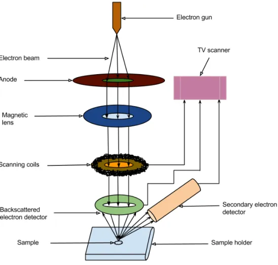
A Scanning Electron Microscope (SEM) is an advanced imaging tool which uses an electron beam instead of light to produce an image. The instrument was developed in the early 1950’s [25] and is now widely used for the mi-croanalysis and 3D imaging of the samles in different research areas. The SEM not only allows the users to magnify an object up to 2000000 times but also reveals the levels of detail and complexity [26] of specimens inaccessi-ble by a traditional light microscope. Since the SEM uses electromagnets to guide and concentrate electrons, it has much larger depth of field and higher degree of resolution rather than any light microscope which uses lenses. A schematic diagram is shown in figure 6 to describe the working principles of a SEM. An electron gun at top of the microscope produces a beam of electrons which passes a vacuum chamber of the microscope and travels a vertical path through electromagnetic (EM) fields and lenses [25]. The EM fields and lenses help the beam to focus down toward the sample and hit the sample to cause to eject electrons and X-rays from it. Detectors of the
microscope collect these backscattered, X-rays and secondary electrons and convert them into a signal. The signal is then sent to a television or computer screen to produce a final image of the investigated regions.
Figure 6: A schematic diagram shows the working principle of a SEM.
1.5
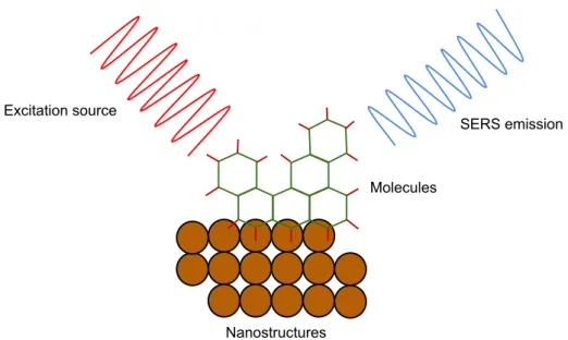
Surface Enhanced Raman Spectroscopy (SERS)
Surface enhanced Raman spectroscopy (SERS) provides the same chemical and structural informations of a molecule that a typical Raman spectroscopy does, but with a greatly enhanced signal [39]. A weak and normal Raman signal can be extremely enhanced by introducing the SERS. This character-ization technique was discovered by Fleischmann, Hendra and Mcquillan in 1974 while they applying Raman spectroscopy to an adsorbate of very high
Raman cross-section, such as pyridine on the silver electrode [39]. However, SERS is a powerful analytical tool which has been widely used in chemical and biological sensing technology over the past decade. This non-destructive technique utilizes plasmonic properties of silver (Ag) and gold (Au) nanopar-ticles in order to detect strong scattered light modulated by atomic vibra-tions within the nanoparticles [18]. This is performed at certain SERS active regions referred to as “hot spots” created at the surafce of the metal nanopar-ticle due to the surface roughness and interparnanopar-ticle spaces. In order to obtain high sensitivity SERS signal, the surface area and roughness of the substrate play a crucial role. A huge surface area enables to adsorb more detection molecules while an appropriate surface roughness increases the “hot spots” on the metal surface. To date, several approaches have been improved to fab-ricate cost-effective, straightforward, multiplex-able and addressable SERS substrates [3, 5]. Most of the SERS substrates are made of nanostructured Au or Ag films which can provide highly sensitive detection. Nowadays, these
substrates are extensively used to prepare semiconducting nanowires, SiO2
nanofibres, aggreated colloids, Au coated TiO2nanotubes, ZnO nanospheres,
nanopolymers and so on [4, 5]. However, it is still a challenge to generate such SERS substrates because of the cost, sensitivity, stability and reproducibility of the substrates need to be taken into account [5]. The vertically aligned CNTs coated with silver have been suggested as Raman signal enhancers since they are stable and can provide simple, low-cost and large-active-area patternable substrates [3, 5]. Accordingly, a further development of SERS substrates is essential to achieve more advanced SERS platforms in the fu-ture. A schematic diagram of a SERS working principle is shown in figure 7.
Excitation source
SERS emission
Molecules
Nanostructures
Figure 7: A schematic diagram shows the working principle of a SERS sys-tem.
1.6
Enhancement Factor of a SERS system
Calculating the value of the SERS enhancement factor (EF ) and number of analyte molecules that contribute to the SERS signal have been confusing the researchers since its discovery. Some previous works [38] related to SERS claimed that the EF was the most important number to characterize a SERS
measurement. The value of a EF ranges from 10 to 1015 [40] depending on
various SERS substrates and how the EF is measured or calculated. The EF calculation procedure for 2D and 3D substrates require different experi-mental setups. In our works, the substrates were 3D and we followed the EF calculation procedure for 3D substrates. The EF of a SERS system can be calculated by using the following formula [31]:
EF = ISERS/NSERS
IRef/NRef
where, ISERS is the peak intensity of a SERS signal, NSERS is the number
of molecules probed on the SERS substrate contributing to the SERS signal,
IRefis the peak intensity of a normal Raman signal and NRef is the number of
molecules probed on the reference region within the laser interaction volume [29-31].
2
Experimental setup and procedure
(i) Photolithography for making patterns onto Si-substrates: In the begining of our work we prepared our samples in a clean room of ISO 5 standard. We choosed silicon-oxide SSP wafers for making suitable transistor patterns onto them. The dimension of each wafer was 3×3 cm and we cut one single wafer into four small pieces by a diamond cutter for patterning. Each small piece was used to make 100 or 50 µm transistor pattern onto it by photolithography. Several small pieces of Si-wafers were organized in a small metal holder and then the holder was put into a beaker which was filled up with acetone. The beaker was put in a ultrasonic cleaner for 20 minutes with keeping the heating process on. After that one new beaker was filled up with methanol and the wafers were moved into it for cleaning them one more time with ultrasonic
cleaner for 20 minutes. The clean wafers were dried by N2 blowing and then
the dried wafers were cleaned again by a plasma cleaner with UV and ozone for 25 minutes. After cleaning by a plasma cleaner, the wafers were fully ready for patterening by photolithography. A photoresist, MICROPOSIT
S1818TM was added to the surface of each wafer and kept them spinning
separately by a spin coater at 4000 rpm ( or 1000 rpm/sec) for one minute.
After that each wafer was hot baked in a portable oven at 110 0C for one
minute. A mask aligner, Karl-Suss MJB3 was used as a source of radiation which produces a typical mercury spectrum with the highest intensity at the H-line (404.7 nm) [7]. The exposure time for the mask aligner was set to 25 seconds. The 50 and 100 µ transistor patterns were pre-printed on an opaque plate which was used as a photomask for patterening. After exposing a high intensity ultraviolet light to the mask, the 50 and 100 µ transistor patterns were burned into the photoresist on the wafers [22]. Then the wafers with 50 µ and 100 µ were put separately in a developer solution for 40 and 60 seconds respectively. The developer solution was made of MICROPOSIT 351 DEVELOPER with a volume ratio to deionized water by 1:5 [7]. The exposed parts of the photoresist were taken away by the developer and the different transistor patterns on the surface of the wafers were clearly visible. The wafers with patterns were then kept in a beaker with distilled water for
in the photolithography technique performed in the clean room is shown in figure 8.
(a) (b) (c)
(d) (e)
Figure 8: (a) Sample cleaning in a plasma cleaner; (b) Creating photoresist thin film onto the clean samples by a spin coater (c) 20, 50 and 100 µm transistor patterns containing photomask; (d) Making transistor patterening onto the substrates by a mask aligner; (e) Developing the samples into a developer solution.
(ii) Physical vapor deposition for depositing buffer and catalyst layer: A thermal evaporator, Kurt J. Lesker Company PVD 75 was employed to de-posite a buffer and catalytic layer onto the wafers. After logging in the system of the evaporator, we pressed “pc vent” button on the pop-up window for venting the PVD chamber. Then we opened the chamber door and took out the substrate holder from the top of the chamber. We moved the substrate shutter out of the way by pressing the button “substrate shutter” while tak-ing out the holder. We placed several wafers in the middle of the round shaped holder by using the clamps and a tungsten boat was set carefully in a specific source without touching any sensor of the chamber. The source shutter was also moved out of the way by pressing the button “source shut-ter” while adding the metal pellets in the tungsten boat. Two small pellets of pure titanium (Ti) were added in the boat for depositing 10 mm buffer layer onto the few wafers. The substrate holder with wafers was placed back
in the chamber and clicked in place. Then we closed the chamber door and pressed “pc pump” button on the pop-up window for pumping the chamber
up to 7.7×10⁻⁸ Torr. We ran a pre-made recipe for Ti with pressing the
button “run recipe” and the metal in the boat started to evaporate when the temperature of the source was high enough. The evaporation rate was monitored by the sensors of the PVD chamber and the whole evaporation process was done in 15-20 minutes. After evaporation of Ti buffer layer, we placed one small pellet pure iron (Fe) and cobalt (Co) each in a new boat for depositing 5 nm catalyst metal layer onto the wafers. Then we followed the same procedure as we introduced for Ti and ran the pre-made recipe for Fe and Co with pressing the button “run recipe”. Once the catalyst metal layer evaporated onto the substrates, the PVD chamber was vented up to 760 Torr for opening its door and the substrate holder was taken out of the chamber with care. After that all of the evaporated wafers were removed from the holder and organized in a metal hoder for placing them in a beaker. The beaker was then filled up with acetone and placed in a ultrasonic cleaner for cleaning the samples for 3 minutes without applying any heat. The re-maining part of the photoresist and metal layer on top of the samples were gone away after cleaning them with acetone. The samples were then moved in an another beaker for cleaning them with distilled water for one minute
and all of the samples were collected after blow-drying with N2. In the last,
the substrate holder was placed back in the PVD chamber and the
cham-ber was pumped again up to 7.7×10⁻⁸ Torr for making it ready for the next
evaporation.
(iii) N-doped CNT growth: In the CVD lab, the evaporated wafers were placed in a quartz tube and the tube was placed in an electric oven. The varigon was kept flowing at a flow rate of 180 ml/min after closing the door of the oven properly. The varigon used in our CVD growth works as a shielding gas for the catalyst particles which keeps them from being oxidized. Then we
started the oven to treat the samples in the tube up to 800 oC with settting
the heat up time 30 minutes. Once the oven reached to 800 oC, the samples
were pre-treated by ammonia (NH3) at a flow rate of 24.8 ml/min for 20
minutes with switching the flow of varigon to 162 ml/min. After treating
the samples with NH3, the flow of varigon was switched back to 180 ml/min
for 3 minutes to remove the N2 gas which usually comes from the previous
NH3 flowing. Then we turned on the flow of pyridine at a rate of 8 µl/min
for 1 hour with setting the varigon flow to 162 ml/min. In our CVD works, pyridine not only is used as a carbon precursor but also plays a vital role for growing N-doped CNTs from the catalyst layer of the Si-substrates. After the
pyridine treatment, the oven was cooled down to 80 oC gradually to prevent
The flow of argon (Ar) at a rate of 179 ml/min was kept flowing instead of the varigon during the whole cooling process. Once the oven reached to 80
oC, the samples were taken out with special care by a long and thin metal
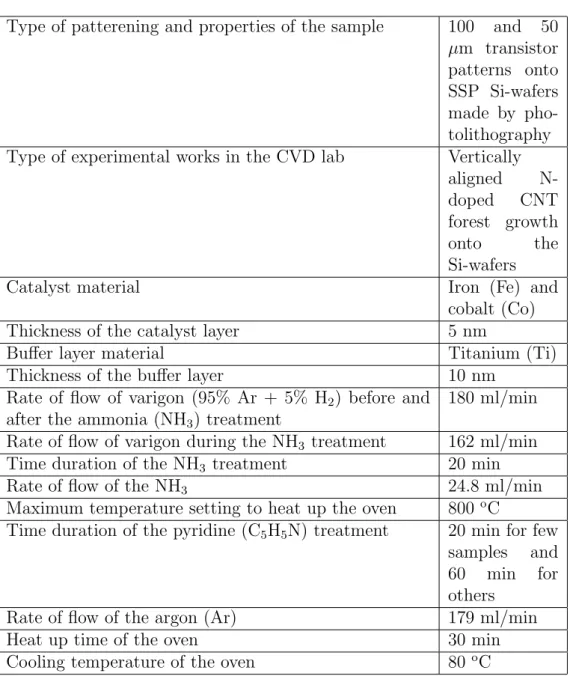
wire hook. All of the parameters used for growing vertically aligned N-doped CNTs onto the Si-substrates in the CVD lab are listed in table 1.
Table 1: The parameters of the vertically aligned N-doped CNT forest growth onto the Si-substrates in the CVD lab
Type of patterening and properties of the sample 100 and 50
µm transistor patterns onto SSP Si-wafers made by pho-tolithography
Type of experimental works in the CVD lab Vertically
aligned
N-doped CNT
forest growth
onto the
Si-wafers
Catalyst material Iron (Fe) and
cobalt (Co)
Thickness of the catalyst layer 5 nm
Buffer layer material Titanium (Ti)
Thickness of the buffer layer 10 nm
Rate of flow of varigon (95% Ar + 5% H2) before and
after the ammonia (NH3) treatment
180 ml/min
Rate of flow of varigon during the NH3 treatment 162 ml/min
Time duration of the NH3 treatment 20 min
Rate of flow of the NH3 24.8 ml/min
Maximum temperature setting to heat up the oven 800 oC
Time duration of the pyridine (C5H5N) treatment 20 min for few
samples and
60 min for
others
Rate of flow of the argon (Ar) 179 ml/min
Heat up time of the oven 30 min
(iv) A silver film deposition on top of the N-doped CNTs: For few samples, a 30 nm silver (Ag) layer was formed on top of the CNTs by running a pre-made recipe for Ag in the thermal PVD process in the clean room. For diffusing Ag nanoparticles along the CNT walls, the Ag-evaporated samples
were placed into a quartz tube and annealed at a temperature of 400 oC in
the electric oven for 30 minutes. The varigon was kept flowing at a rate of 180 ml/min during the annealing time and after the heat treatment, the oven
was cooled down to 80 oC with keeping the flow of Ar instead at a rate of
179 ml/min.
(v) A gold film deposition on top of the N-doped CNTs: A few samples were placed in the substrate holder of the PVD chamber in order to deposit a 30 nm gold (Au) film onto the CNTs. The evaporation was done in the clean room by running a pre-made recipe for Au in the thermal PVD process. The gold nanoparticles were diffused along the CNT walls by the annealing
at a temperature of 800 oC for 10 minutes. The varigon flow at a rate of
180 ml/min was introduced during the heating time and the pure Ar gas was kept flowing instead at a rate of 179 ml/min while cooling down the oven to
80 oC.
(vi) Scanning Electron Microscope (SEM) Measurements: A Carl Zeiss Mer-lin Field Emission Scanning Electron Microscope (FESEM) [23] was used to investigate the Ag and Au nanoparticles size and distribution along the CNT
walls. Each Ag and Au sample was tilted 45o to check out the density and
height of the CNT forest onto their surfaces. Firstly, the samples were orga-nized in a sample holder and the holder was placed in the vacuum chamber of
the SEM. The chamber was pumped to 10-6 mbar by the SmartSEM V.5.06
[23] software to make the SEM ready for the measurements. For a single measurement, the settings of the SEM were as follows:
Probe current: 150 pA; Magnification: 1K - 2000000×; Working Distance (WD): 5.4 nm; Noise Reduction: Replacing a single pixel by the average of pixels; Type of electrons used in imaging: Secondary Electrons (SE) and Backscattered Electrons (BSE); Detector of the system: In Lens; Extra High Tension (EHT) voltage: 4 kV; Energy Selective Backscattered (ESB) grid
voltage: 350V; System vacuum: 2.13×10⁻⁶ mbar.
(vii) Substrate characterization by the surface enhanced Raman spectroscopy
(SERS): In our works, the final measurements were made by a RENISHAWTM
inVia confocal Raman microscope [24] with using a 785 nm of the excitation wavelength. For each sample, the exposure time was set to 10 seconds for collecting the spectra from the top view of the CNTs with using an objective 50×/0.75. To find the high density of Au nanoparticles onto the CNTs, a laser power of 12.5 µW out of a total power of 25mW was used with set-ting the acuumulations to 1. To find the “hot spots” created by the Ag
nanoparticles, the laser power switched to 25 nW with accumulations 3 as the SERS spectras were oversaturated at the previous laser power used for the Au samples. For high resolution mapping, 72 points onto the Ag- and Au-coated CNT surface were scanned at the laser power of 25 nW with set-ting the value at accumulation number 1 and step size number 1. To enhance the Raman signals, the solution of 4-aminothiophenol (4-ATP) with different concentrations were made for both Ag and Au samples. In our works, the 4-ATP solution was also used as a SERS probe molecule [4] to calculate the SERS enhancement factor. A 10 fM, 10 pM, 10 nM, 10 µM and 200 µM of different ethanolic concentrations of 4-ATP solution were prepared in sev-eral small beakers in the CVD lab and each sample was immersed into these solutions from lower to higher concentration for every 1 hour with covering the beakers by a parafilm and aluminium foil paper as the 4-ATP is a light sensitive material. The settings of the Raman microscope during the SERS measurements were as follows:
Objective: 50×/0.75, Measurement type: Confocal; Tray position: 0.1 µm; Imaging type: High-speed streamline imaging; Type of mapping: Mapping image acquisition; Excitation source: 785 nm infrared diode laser.
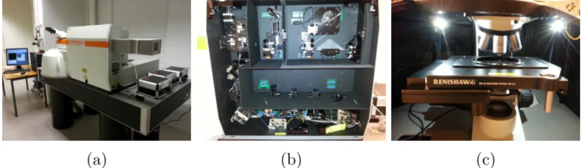
The inVia Raman microscope applied to make the final measurements is shown in figure 9.
(a) (b) (c)
Figure 9: (a) RENISHAWTM inVia confocal Raman microscope with CCD
detector; (b) Different optical components of the Raman microscope: notch filter, diffraction grating, laser tunning mirror, beam expander, slit, etc; (c) Different objectives and a translation stage of the spectrometer.
3
Results
3.1
Vertically aligned N-doped CNT forest growth onto
the substrates
Overview pictures of vertically aligned N-doped CNT forest onto 100, 50 and 20 µm transistor patterns with and without containing a 10 nm Ti-buffer layer under the catalyst layer can be seen in figure 10 a-e.
(a) (b) (c)
(d) (e)
Figure 10: Vertically aligned N-doped CNT forest onto the transistor pat-terns of (a) 100 µm with having a 10 nm Ti-buffer layer under the Fe+Co layer; (b) 50 µm with having a 10 nm Ti-buffer layer under the Fe+Co layer; (c) 100 µm without having any buffer layer under the Fe+Co layer; (d) 50 µm without having any buffer layer under the Fe+Co layer; (e) 20 µm without having any buffer layer under the Fe+Co layer.
Figure 10 shows the vertically aligned N-doped CNT forest growth onto Si-substrates through the CVD process. The CNT forests look promising as the parameters related to the CVD process worked very well. The narrow space between two forest lines is easily visible to the naked eyes for 100 and 50 µm of transistor patterns whether 20 µm requires an optical microscope. Additionally, some top-view high resolution SEM pictures of the vertically aligned N-doped CNT forest onto different transistor patterns with and with-out having a buffer layer under the catalyst metal layer are also shown in
figure 11 a-d.
(a) (b)
(c) (d)
Figure 11: Top-view SEM images onto the transistor patterns of (a) 100 µm with having a 10 nm Ti-buffer layer under the catalyst layer, The scale bar is 200 µm; (b) 100 µm without having any buffer layer under the catalyst layer, The scale bar is 100 µm; (c) 50 µm with having a 10 nm Ti-buffer layer under the catalyst layer, The scale bar is 100 µm; (d) 20 µm without having any buffer layer under the catalyst layer, The scale bar is 200 µm.
It is clearly seen from figure 11 that transistor pattern allows the CNTs to grow up only from that surface through the CVD process wherein the catalyst metal particles are present. The SEM images also show the edges of each pattern whereon the CNTs have been grown up are very sharp. However, it seems that Ti-buffer layer doesn’t affect CNT growth from the catalyst layer (Fe+Co) and probably it protects the catalyst metal particles from being diffused into the substrate surface. Some previous works [27] related to use a buffer layer onto the Si-substrates showed that the buffer layer increased the uniformity and growth time of the CNT compared with the case while using no buffer layer. It can also be seen in 11 that some part of
the patterns have been damaged and it is believed that the damage arises from the photolithography technique. In the photolithography process, the develpoing time was too long for some samples as some photoresist had been dissolved into the developer solution which were not exposed to UV radiation.
Two samples of 100 and 20 µm transistor patterns were tilted 45o to see the
cross-sectional SEM view of N-doped CNT forest and the images are shown in figure 12.
(a) (b)
Figure 12: Cross-sectional SEM view of the N-doped CNT forest onto
tran-sistor patterns of (a) 100 µm tilted 45o, The scale bar is 200 µm; (b) 20 µm
tilted 45o, The scale bar is 100 µm.
In figure 12, since the CNTs onto the patterns look stable, promising and detailed, the route to grow up CNTs from the catalyst layer is successful through the CVD process. It is also clear that the catalyst metal particles remain undamaged during the high temperature heat treatment in the CVD process and therefore no particle is diffused into the substrate surface.
3.2
N-doped CNT forest characterization through the
SEM imaging
High resolution top-view SEM pictures of the CNT forest onto different tran-sistor patterns are shown in figure 13. In each SEM picture, the top surface of a Si-substrate look very clean and the SEM observations also confirm that no particles diffusion has occoured into the substrate surface during the CVD process. As it is hard to examine the alignment, height and density of the CNT forest through top-viewing, the cross-sectional images are needed instead to study these properties thoroughly.
(a) (b)
(c) (d)
Figure 13: Top-view SEM pictures of N-doped CNT forest onto the transistor patterns of (a) 100 µm, The scale bar is 100 µm; (b) 100 µm, The scale bar is 20 µm, (c) 20 µm, The scale bar is 20 µm; (d) 20 µm, The scale bar is 10 µm.
The cross-sectional SEM images of N-doped CNT forests grown onto the transistor patterns of 100, 50 and 20 µm after applying different pyridine treatment times during the CVD process are given in figure 14. Moreover, figure 14 also shows some N-doped CNT forests whose had no buffer layer; on the other hand, a 10 nm of Ti-buffer layer was applied for the others.
(a) (b)
(c) (d)
(e) (f)
Figure 14: Cross-sectional SEM pictures of N-doped CNT forests onto the
transistor patterns of (a-b) 100 µm tilted 45o, no buffer layer, pyridine
treat-ment time is 60 minutes, The scale bar is 20 µm; (c) 100 µm tilted 45o, 10
nm Ti-buffer layer, pyridine treatment time is 20 minutes, The scale bar is
10 µm; (d) 50 µm tilted 45o, 10 nm Ti-buffer layer, pyridine treatment time
is 20 minutes, The scale bar is 10 µm; (e-f) 20 µm tilted 45o, 10 nm Ti-buffer
It is seen in figure 14 that the height of N-doped CNT forests grown with the longer pyridine treatment time is around 41 µm, whereas the height of others grown with the shorter pyridine treatment time is 20 µm. A pyridine is commonly used as a precursor to synthesis N-doped CNTs through the CVD process and the use of it allows a controlled doping of nitrogen (N) on the catalyst metal surface. The rate of N-doping on the catalyst surface increases
if a regulated steam of NH3 is intoduced in the CVD process along with the
pyridine precursor [28]. However, pyridine treatment time determines the height of N-doped CNT forest which is grown by CVD process. It can also be seen in figure 14 that the density of N-doped CNT forest grown from the catalyst surface without having a buffer layer is much lower than the N-doped forest grown from the same catalyst surface with having a 10 nm Ti-buffer layer. The less dense CNT forest proves that the rate of catalyst particles loss into the substrate surface is high as no protection layer has previously formed on that surface. The rate of catalyst particles loss into the silicon surface can be minimized by depositing a buffer layer onto that surface. On the contrary, the N-doped CNT forests whose don’t have any buffer layer are more aligned in straight direction than the other N-doped forests whose had a 10 nm buffer layer. Apparently, the density of catalyst particles into the Si-surface without having a buffer layer is much less compared with the surface with having a buffer layer. Anyway, the CNTs can grow up from the surface inwhere the catalyst particles density is low but the CNT growth has less opportunity to get stuck with the particles and every single CNT gets enough space to align vertically. In other case, when the catalyst particles density is high, the CNTs collide with more particles while growing up from the catalyst surface and as a result, the CNT alignment comes out is not very vertical. To examine how the N-doped CNT forest look like after peeling a transistor pattern off, a 20 µm pattern was peeled off by a sticky tape and top view SEM images of the N-doped CNT forests are given in figure 15.
(a)
(b)
Figure 15: (a) Top-view SEM picture of N-doped CNT forest after peeling a 20 µm transistor pattern off by a sticky tape. No buffer layer was applied on the substrate surface and the pyridine treatment time was 60 minutes during the CVD process, The scale bar is 20 µm; (b) Top-view SEM image shows the remain N-doped CNT forest onto 20 µm transistor pattern after peeling the pattern off. No buffer layer was applied on the substrate surface and the pyridine treatment time was 60 minutes during the CVD process, The scale bar is 100 µm.
It can be seen in figure 15 that the N-doped CNT forest look promising even no buffer layer was applied on the substrate surface. A buffer layer can only be used to make the CNT forest dense as a dense forest is much more capable to create the “hot spots” after diffusing Ag and Au nanoparticles on top of it. The “hot spots” are created along the CNT forest as Ag and Au have plasmonic properties which make the field enhancement factor maxi-mum in the CNT surface. The SERS signals from the “hot spots” are the strongest and our main goal is to achieve it. To create a dense CNT forest, one should use a buffer layer on the substrate surface before evaporating a catalyst metal layer on top it.
3.3
SEM image characterization after evaporation of
the Ag and Au metal layer on the N-doped CNT
forest
Cross-sectional (tilted 45o) SEM images of N-doped CNT forest after
evap-orating a 30 nm of Ag metal layer onto it are given in figure 16. In figure 16, one can see no Ag nanoparticle has formed along the CNT wall as no annealing process was applied in the forest. The forests grown with longer and shorter pyridine treatment time during the CVD process look dense as a 10 nm Ti-buffer layer was deposited on the substrate surface. If we look at more zoomed SEM pictures, every single CNT orientation in the forest is clearly visible. The outer surface of each CNT look very rough as it was covered by Ag particles during the evaporation process and the tube diam-eter ranges from 50 to 100 nm. A single CNT which has a outer surface covered by Ag or Au particles can create a very small gap between two metal nanoparticles and thus the “hot spots” can be formed through the annealing process. Therefore, one can obtain the strongest possible SERS signal from the “hot spots” only.
(a) (b)
(c) (d)
(e) (f)
Figure 16: (a) Cross-sectional SEM pictures of N-doped CNT forest after evaporating a 30 nm of Ag layer onto it. Parameters of the forest: Height : 41 µm, Buffer layer: 10 nm Ti, Pyridine treatment time: 60 min, Scale bar: 10 µm; (b) Cross-sectional SEM pictures of single CNT orientation in the forest, Parameters of CNT: Diameter range: 50-100 nm, Buffer layer: 10 nm Ti, Pyridine treatment time: 60 min, Scale bar: 200 nm; (c) Cross-sectional SEM pictures of N-doped CNT forest after evaporating a 30 nm of Ag layer onto it. Parameters of the forest: Height : 10 µm, Buffer layer: 10 nm Ti, Pyridine treatment time: 20 min, Scale bar: 10 µm; (d-f) Cross-sectional SEM pictures of single CNT orientation in the forest; Parameters of CNT: Diameter range: 50-100 nm; Buffer layer: 10 nm Ti; Pyridine treatment time: 20 min, Scale bar: 200, 200 and 100 nm.
Cross-sectional (tilted 45o) and top-view SEM images of N-doped CNT
17. As seen in figure 17, the N-doped CNT forest with having a 35 nm of Au layer look also dense, vertical and promising. As no annealing process was applied in the forest, the Au nanoparticles diffusion has not occurred along the CNT walls. In the zoomed SEM images, the orientation of every single CNT in the forest is clearly distinguishable.
(a) (b)
(c) (d)
(e) (f)
Figure 17: (a-b) Cross-sectional SEM pictures of N-doped CNT forest after evaporating a 35 nm of Au layer onto it. Parameters of the forest: Height: 10 µm, Buffer layer: 10 nm Ti, Pyridine treatment time: 20 min, Scale bar: 10 µm; (c) Top view SEM picture of N-doped CNT forest after evaporating a 35 nm of Au layer onto it. Parameters of the forest: Buffer layer: 10 nm Ti, Pyridine treatment time: 20 min, Scale bar: 10 µm; (d-f) Cross-sectional SEM pictures of single CNT orientation in the Au-coated forest; Parameters of CNT: Diameter range: 50-100 nm, Buffer layer: 10 nm Ti, Pyridine treatment time: 20 min, Scale bar: 200, 200 and 100 nm.
In figure 17, the outlook for the outer surface of a single tube is rough as the surface was covered by Au particles during the PVD process. The diameter of a tube varies from 50 to 100 nm. It has already discussed before the tubes having rough outer surfaces can create more “hot spots” for the SERS measurement. If we look at the tube outer surface in figure 17 d-f, it seems there is a strong probability to get the strongest possible SERS signal from the surface onwhere the “hot spots” can be created by Au or Ag nanoparticles.
3.4
SEM image characterization after annealing of the
Ag and Au metal layer on the N-doped CNT forest
For diffusing Ag nanoparticles along the CNT walls, the samples with 100
µm transistor patterns were annealed at a temperature of 400 oC for 30
minutes in the CVD oven. Top-view and cross-sectional (tilted 45o) SEM
images of N-doped CNT forest and the Ag nanoparticles distribution along the CNT walls are given in figure 18. One can see in figure 18 that the annealing process creates a high density of Ag nanoparticles along the CNT walls. The annealing process was applied to two different forest heights as the pyridine treatment times were different while growing these forests through the CVD process. The pyridine treatment times were 60 and 20 minutes for the longer (height 41 µm) and shorter (height 10 µm) forests respectively. In both forests (41 and 10 µm), the size of Ag nanoparticles varies from 200 to 600 nm. The Ag nanoparticles distribution in the forest and on the catalyst metal surface look homogeneous. Figure 18 also confirms that the density of Ag nanoparticles along the CNT walls is much lower than the density of Ag nanoparticles on top of the forest. The formation of Ag nanoparticles on the CNT surface depends on the diffusion barrier, surface wetting and nucleation rate of Ag particles [4]. Ag particles have low diffusion barrier, weak surface wetting and high nucleation rate with the CNTs. Each tube to tube intersection creates a high nucleation rate for Ag particles and the discrete Ag nanoparticles with having samll gaps between them are formed on the CNT surface [4]. The result is the “hot spots” on that surface from where one can get the strongest SERS signal.
(a) (b)
(c) (d)
(e) (f)
Figure 18: (a-c) Cross-sectional SEM pictures of the Ag-coated N-doped longer, shorter and longer CNT forests after 30 minutes of annealing at 400
oC. Forest properties: Height: 41 µm (longer), 10 µm (shorter); The scale bar
is 10 µm. (d-e) Top-view SEM pictures of the Ag nanoparticles distribution on top of the shorter and longer N-doped CNT forests. The scale bar is 2 and 10 µm. (f) Top-view SEM picture of the Ag nanoparticles distribution on the catalyst surface. The scale bar is 10 µm.
For the Au nanoparticles diffusion on top of the N-doped CNT forest and along the tubes, the samples of 100 µm transistor patterns were annealed at
a temperature of 800 oC for 10 minutes in the CVD oven. Several top-view
and cross-sectional (tilted 45o) SEM images of N-doped CNT forest and the
Au nanoparticles distribution on top it and along the tubes are shown in figure 19. As seen in figure 19, the N-doped CNT forest was grown from the catalyst surface with a pyridine treatment time of 20 minutes through
the CVD process. The height of the forest is 10 µm and the size of Au nanoparticles in the forest varies from 50 to 100 nm. According to figure 19, the Au nanoparticles distribution in the forest look very homogeneous and the density of Au nanoparticles on top of the forest is much higher compared along the tube walls. Therefore, Au has a low diffusion barrier, weak surface wetting and high nucleation rate with the CNTs which are related to form Au nanoparticles on the CNT surface [4]. Each tube to tube intersection makes a high nucleation rate for Au to form nanoparticles on the CNT surface and the distinct Au nanoparticles with having small gaps between them are created along the tube walls [4]. The “hot spots” are then formed on the CNT surface and the SERS signal from that surface is the strongest.
(a) (b)
(c) (d)
Figure 19: (a) Cross-sectional SEM image of the Au-coated N-doped CNT
forest after 10 minutes of annealing at 800 oC. The forest height is 10 µm.
The scale bar is 10 µm. (b-c) Top-view SEM images of the Au nanoparticles distribution on top of the N-doped CNT forest. The scale bar is 1 µm and 100 nm. (d) Cross-sectional SEM image of the Au nanoparticles diffusion along the CNT walls. The scale bar is 200 nm.
3.5
The SERS measurements
To get the enhanced SERS signals from the vertically aligned Ag-coated N-doped CNT forest, an as-prepared sample was exposed to 10 fM ethanolic 4ATP solution first. The SERS measurement was carried out from the top surface of the sample and the SERS spectra for this measurement is shown in figure 20 a. The enhanced SERS signals of the D and G band of N-doped MWCNTs covered by the Ag nanoparticles are seen in figure 20 a. As seen in
figure 20 a, the peak intensity at wave number of 1076 cm-1is 6000 cps (counts
per second). As soon as the 4ATP solution has evaporated, the surface ten-sion of ethanol and strong van der Waals forces of the molecules are summed together to get stuck with the CNTs to a near-ideal graphite spacing [4]. This causes to decrease the lateral dimension of CNTs by 19% from the as-grown CNTs [4]. The squeezed CNTs cause a dramatic increase the density of Ag nanoparticles on their surfaces. The result is an increased number of “hot spots” on the CNT surface and the SERS signals from these “hot spots” are the strongest. Subsequently, the same sample was exposed to 10 pM, 10 nM, 10 µM and 200 µM ethanolic 4ATP solution to observe the change in SERS spectras. Figure 20 b-e shows the different SERS spectras from the vertically aligned N-doped CNT forest with diffused Ag nanoparticles after exposing it to 10 pM, 10 nM, 10 µm and 200 µm ethanolic 4ATP solution. Each single SERS measurement was carried out from the top surface of the sample.
Wave number in cm-1
200 400 600 800 1000 1200 1400 1600 1800 2000
Counts or intensity (a.u.)
0 5000 10000 15000 10 fM (a) Wave number in cm-1 200 400 600 800 1000 1200 1400 1600 1800 2000
Counts or intensity (a.u.)
0 5000 10000 15000 20000 10 pM (b) Wave number in cm-1 200 400 600 800 1000 1200 1400 1600 1800 2000
Counts or intensity (a.u.)
×104 0 0.5 1 1.5 2 2.5 10 nM (c) Wave number in cm-1 200 400 600 800 1000 1200 1400 1600 1800 2000
Counts or intensity (a.u.)
×104 0 1 2 3 4 10 µM (d) Wave number in cm-1 200 400 600 800 1000 1200 1400 1600 1800 2000
Counts or intensity (a.u.)
×104 0 1 2 3 4 5 6 7 200 µM (e)
Figure 20: The SERS spectras from the vertically aligned N-doped CNT forest with Ag nanoparticles. Raman instrument settings: Laser: 785 nm infrared diode; Laser power: 0.0001%; Accumulations: 3; Exposure time: 10 s; Objective: 50×/0.75. Forest properties: Height: 10 µm; Patterns: 100 µm transistor; Pyridine treatment time: 20 mins; Annealing temperature and
time: 400 oC, 30 mins. (a) SERS spectra with 10 fM ethanolic 4ATP. The
peak intensity at wave number of 1076 cm-1 is 6000 cps. (b) SERS spectra
with 10 pM ethanolic 4ATP. The peak intensity at wave number of 1076
cm-1 is 19000 cps. (c) SERS spectra with 10 nM ethanolic 4ATP. The peak
intensity at wave number of 1076 cm-1 is 2.4×10⁴ cps. (d) SERS spectra
with 10 µM ethanolic 4ATP. The peak intensity at wave number of 1076
cm-1is 4×10⁴ cps. (e) SERS spectra with 200 µM ethanolic 4ATP. The peak
One can also see the enhanced SERS signals of the D and G band of N-doped MWCNTs in figures 20 b-e. The peak intensities at wave number
of 1076 cm-1 in figures 20 b-e are 19000 (10 pM 4ATP), 2.4×10⁴ (10 nM
4ATP), 4×10⁴ (10 µM 4ATP) and 6×10⁴ (200 µM 4ATP) cps respectively.
To see the SERS spectra variations with different 4ATP concentraions, the spectras from figure 20 are combined together in figure 21.
Wave number in cm-1
200 400 600 800 1000 1200 1400 1600 1800 2000
Counts or intensity (a.u.)
×104 0 1 2 3 4 5 6 7 10 fM 10 pM 10 nM 10 µM 200 µM Ag trend curves
Figure 21: Combination of the 4ATP concentration dependent SERS spectras of N-doped MWCNTs with Ag nanoparticles.
Figure 21 clearly shows that the peak intensity at wave number of 1076
cm-1 increases with higher concentration of 4ATP solution. To see the
Ag-trend curves with different concentrations of 4ATP solution, the inset region of figure 21 was plotted in MATLAB separately. The 4ATP concentration dependent Ag-trend curves are shown in figure 22.
Wave number in cm-1
1030 1040 1050 1060 1070 1080 1090 1100 1110 1120
Counts or intensity (a.u.)
×104 0 1 2 3 4 5 6 7 10 fM 10 pM 10 nM 10 µM 200 µM 1 mM (Bulk)
Figure 22: 4ATP concentration dependent Ag-trend curves.
It is clear from figure 22 that the characteristic peak of every SERS
spec-tra at 1076 cm-1 represents the 4ATP concentration dependent Ag-trend
curves. Additionally, a SERS spectra from 1mM 4ATP solution placed on a silicon surface is added in the presented Ag-trend curves. No peak is ob-served in the SERS spectra from this bulk material as it has not applied to a CNT surface. To draw a calibration curve between the peak intensity and concentration of 4ATP, the peak intensities of 10 fM, 10 pM, 10 nM, 10 µM
and 200 µM 4ATP at 1076 cm-1 were plotted against their corresponding
Concentration of 4ATP 200 µM 10 µM 10 nM 10 pM 10 fM Peak intensity at 1076 cm -1 ×10⁴ 0 1 2 3 4 5 6
Figure 23: The peak intensities of 4ATP at 1076 cm-1.
For the SERS enhancement, it is seen in figure 23 that the peak
intensi-ties of the SERS spectras at 1076 cm-1 in each concentration of 4ATP could
attain up to the lowest detection limit 10 fM without any surface chemistry of CNTs [4]. The laser power also relates to the SERS enhancement as the higher power can provide more characteristic signals at lower concentration of 4ATP.
To get enhanced SERS signals from the N-doped CNT forest with Au nanoparticles through annealing, the as-prepared sample was exposed to 10 fM ethanolic 4ATP solution. The laser was focused on the top surface of the sample and the SERS spectra for this measurement is shown in figure 24 a. The enhanced SERS signals of the D and G band of vertically aligned N-doped CNTs with Au are seen in figure 24 a. Figure 24 a also shows
the peak intensity at wave number of 1076 cm-1 is 4100 cps. Furthermore,
the same sample was exposed to 10 pM, 10 nM and 10 µM ethanolic 4ATP solution to observe the change in SERS spectras. Figures 24 b-d show the different SERS spectras from the Au-coated vertically aligned N-doped CNT forest after exposing it to 10 pM, 10 nM and 10 µm ethanolic 4ATP solution.
For the SERS measurement, the laser was focused on the top surface of the sample and the SERS spectras were collected afterwards.
Wave number in cm-1
200 400 600 800 1000 1200 1400 1600 1800 2000
Counts or intensity (a.u.)
0 2000 4000 6000 8000 10000 12000 14000 10 fM (a) Wave number in cm-1 200 400 600 800 1000 1200 1400 1600 1800 2000
Counts or intensity (a.u.)
0 5000 10000 15000 10 pM (b) Wave number in cm-1 200 400 600 800 1000 1200 1400 1600 1800 2000
Counts or intensity (a.u.)
0 5000 10000 15000 10 nM (c) Wave number in cm-1 200 400 600 800 1000 1200 1400 1600 1800 2000
Counts or intensity (a.u.)
×104 0 0.5 1 1.5 2 2.5 3 10 µM (d)
Figure 24: The SERS spectras from the vertically aligned N-doped CNT forest with Au nanoparticles. Raman instrument settings: Laser: 785 nm infrared diode; Laser power: 0.05%; Accumulations: 1; Exposure time: 10 s; Objective: 50×/0.75. Forest properties: Height: 10 µm; Patterns: 100 µm transistor; Pyridine treatment time: 20 mins; Annealing temperature and
time: 800 oC, 10 mins. (a) SERS spectra with 10 pM ethanolic 4ATP. The
peak intensity at wave number of 1076 cm-1 is 4100 cps. (b) SERS spectra
with 10 pM ethanolic 4ATP. The peak intensity at wave number of 1076
cm-1 is 7000 cps. (c) SERS spectra with 10 nM ethanolic 4ATP. The peak
intensity at wave number of 1076 cm-1 is 11100 cps. (d) SERS spectra with
10 µM ethanolic 4ATP. The peak intensity at wave number of 1076 cm-1 is
2.6×10⁴ cps.
The enhanced SERS signals of the D and G band of Au-coated verti-cally aligned N-doped CNTs are also observed in figures 24 b-d. The peak
intensities at wave number of 1076 cm-1 in figures 24 b-d are 7000 (10 pM
4ATP), 11100 (10 nM 4ATP) and 2.6×10⁴ (10 µM 4ATP) cps respectively.
To see the alteration in SERS spectras with different 4ATP concentraions, the spectras from figure 24 are combined together in figure 25.
Wave number in cm-1
200 400 600 800 1000 1200 1400 1600 1800 2000
Counts or intensity (a.u.)
×104 0 0.5 1 1.5 2 2.5 3 10 fM 10 pM 10 nM 10 µM Au trend curves
Figure 25: Combination of the 4ATP concentration dependent SERS spectras of N-doped MWCNTs with Au nanoparticles.
As seen in figure 25, the peak intensity at wave number of 1076 cm-1
increases with higher concentration of 4ATP solution. A simple comparison between figures 21 and 25 shows that the SERS signal from the CNT forest with Ag nanoparticles is much stronger than the SERS signal from Au-coated CNT forest. The Au particles are more stable than Ag as the Ag particles have the tendency to become oxidized in air. Sometimes, the SERS signals from the “hot spots” created by silver nanoparticles can rise up to 3 times than the signals from the “hot spots” created by gold nanoparticles [18]. To see the Au-trend curves with different concentrations of 4ATP solution, the inset region of figure 25 was plotted in MATLAB separately. The 4ATP concentration dependent Au-trend curves are shown in figure 26.
Wave number in cm-1
1040 1050 1060 1070 1080 1090 1100 1110 1120
Counts or intensity (a.u.)
×104 0 0.5 1 1.5 2 2.5 3 10 fM 10 pM 10 nM 10 µM 1 mM (Bulk)
Figure 26: 4ATP concentration dependent Au-trend curves.
One can see in figure 26 that the characteristic peak of every SERS spectra
at 1076 cm-1represents the 4ATP concentration dependent Au-trend curves.
In addition, a SERS spectra from 1mM 4ATP solution placed on a silicon surface is added in the presented Au-trend curves. Obviously no peak is observed in the SERS spectra from this bulk material since it has not applied to a CNT surface. To draw a calibration curve between the peak intensity and concentration of 4ATP, the peak intensities of 10 fM, 10 pM, 10 nM
and 10 µM 4ATP at 1076 cm-1 were plotted against their corresponding
Concentration of 4ATP 10 µM 10 nM 10 pM 10 fM Peak intensity at 1076 cm -1 ×10⁴ 0 0.5 1 1.5 2 2.5 3
Figure 27: The peak intensities of 4ATP at 1076 cm-1.
As seen in figure 27, the generated vertically aligned N-doped CNT forest has provided a stable platform to generate highly dense “hot spots” on the CNT surface for the SERS measurement. Since the SERS signal enhancer decreases the space between CNTs, the coupling between Au nanoparticles and CNTs is increased what causes highly concentrated Au nanoparticles on the CNT surface [3]. Further, the “hot spots” are created on this surface, whereupon the strongest SERS signals are observed during the measurement.
3.6
The SERS mapping
To study the enhanced SERS signal uniformity, SERS mapping was per-formed on the N-doped CNT forest with Ag nanoparticles through annealing. Firstly, the sample was exposed to 10 µM 4ATP solution for one hour and then air-dried. A suitable region of a CNT surface in a regular array (X and Y) was choosed to perform the mapping with 785 nm infrared diode laser. Figure 28 shows the SERS mapping image, optical image of mapping region
and SERS mapping spectra.
(a)
(b) (c)
Figure 28: The SERS mapping performance outputs. Mapping type: Map image acquisition. The Raman instrument settings: Laser: 785 nm infrared diode; Laser power: 0.0001%; Objective: 50×/0.75; Accumulations: 1; Expo-sure time: 10 s; Step size: 1; Number of scanned points: 72. N-doped CNT forest properties: Height: 10 µm; Patterns: 100 µm transistor; Pyridine treatment time: 20 mins; Diffused nanoparticles: Ag; Annealing
tempera-ture and time: 400 oC, 30 mins; Analyte solution: 10 µM ethanolic 4ATP.
(a) The SERS mapping image. (b) The optical image of mapping region. (c)
The SERS mapping spectra. The relative peak intensity at 1076 cm-1is 3200
The resulting SERS map (figure 28) comprises of 72 spectras and shows
the relative peak intensity at 1076 cm-1 is 3200 cps. It is seen that the
SERS signals from Ag-coated N-doped CNT forest are relatively uniform even though some darker regions appear in mapping. The darker regions during the SERS mapping occur due to the leaning of CNTs [29] and lack of “hot spots” on the CNT surface. However, the presented SERS mapping demonstrates the coupling between CNTs and Ag nanoparticles at the par-tition area which increases the effectiveness significantly to detect an organic molecule in a short measurement time [30].
To investigate the enhanced SERS signal uniformity, SERS mapping was performed on the N-doped CNT forest covered by the Au nanoparticles through annealing. Initially, the sample was exposed to 10 µM 4ATP solu-tion for one hour and then air-dried. To establish a coherent SERS mapping on the CNT surface covered by the Ag and Au nanoparticles, the same laser power was employed in both cases. A suitable region of the CNT surface in a regular array (X and Y) was choosed to perform the mapping with 785 nm infrared diode laser. Figure 29 shows the SERS mapping image, optical image of mapping region and SERS mapping spectra.
(a)
(b) (c)
Figure 29: The SERS mapping performance outputs. Mapping type: Map image acquisition. The Raman instrument settings: Laser: 785 nm infrared diode; Laser power: 0.0001%; Objective: 50×/0.75; Accumulations: 1; Expo-sure time: 10 s; Step size: 1; Number of scanned points: 72. N-doped CNT forest properties: Height: 10 µm; Patterns: 100 µm transistor; Pyridine treatment time: 20 mins; Diffused nanoparticles: Au; Annealing
tempera-ture and time: 800 oC, 10 mins; Analyte solution: 10 µM ethanolic 4ATP.
(a) The SERS mapping image. (b) The optical image of mapping region. (c)
The SERS mapping spectra. The relative peak intensity at 1076 cm-1 is 900
cps.
relative peak intensity at 1076 cm-1 is 900 cps. A comparison between two maps presented here shows a CNT surface covered by the Au nanoparticles is more homogeneous compared with a surface covered by the Ag nanoparticles. As described before, a SERS signal from the “hot spots” created by the Ag nanoparticles is much stronger compared with a signal from the “hot spots” created by the Au nanoparticles. However, the two maps confirm the Au nanoparticles distribution on a CNT surface is more uniform and stable but contains less dense “hot spots” than a Ag-coated CNT surface.
3.7
Enhancement Factor of the SERS system
The laser interaction volume was determined by using the method described in [29]. Firstly, a SERS substrate was placed in the focal plane of Raman microscope and then it was moved vertically out of the focal plane at an increment of 1 µm each. The SERS signal for each vertical movement (z-direction) was summed and normalized by the maximum peak intensity at
the focal plane. The measured laser interaction volume was 48 µm3 after
applying the excitation source of 785 nm infrared diode laser whose spot size was 1.28 µm. The 50×/0.75 objective and 0.0001% laser power were em-ployed in this measurement.
To calculate the value of IRef:
200 µM ethanolic 4ATP was prepared in small beaker and then poured into a petri dish. With using the excitation source of 785 nm infrared diode laser,
50×/0.75 objective and 0.0001% laser power, the measured value of IRef was
2 cps at 1076 cm-1.
To calculate the value of NRef:
With using the laser interaction volume of 48 µm3, the value of N
Ref was
estimated to be 6×10⁹.
To calculate the value of ISERS:
A sample with 100 µm transistor pattern and consisted of N-doped CNT forest with Ag nanoparticles through annealing was immersed into 200 µM ethanolic 4ATP solution for one hour. Hereafter, the sample was air-dried and placed in the Raman microscope. The 785 nm infrared diode laser, 50×/0.75 objective lens and 0.0001% laser power were applied to calculate
the value of ISERS. The calculated value of ISERS was 60000 cps at 1076 cm-1.
The number of 4-ATP molecules within the area of laser spot was
esti-mated by considering a monolayer of 4-ATP (∼ 6˚A) [32] on the substrate
surface. In this calculation, the packing density of 4-ATP was assumed to
be 0.20 molecules/nm2 [32]. After taking the CNT surface topography into
consideration while using the laser spot size of 1.28 µm, the area of the
effec-tive region probed by the laser was 6.4 µm2. The estimated value of N
SERS
was 2×10⁷.
Thus we can calculate the EF for the SERS measurement from equation (1) as
EF = 60000/2×107
2/6×109 = 9×10 6.
This is the enhancement factor for the SERS measurement applies to Ag-coated N-doped CNT forest. To calculate the EF in the case of Au-Ag-coated N-doped CNT forest, the EF calculation procedure as described above was followed. For this measurement, we obtained the following parameters:
IRef= 1 cps at 1076 cm-1; NRef= 6×10⁹; ISERS= 900 cps at 1076 cm-1 and
NSERS= 2×10⁷.
Hence, the EF for the SERS measurement applies to Au-coated N-doped CNT forest can also be calculated from equation (1) as
EF = 900/2×107
1/6×109 = 2.7×10 5.
4
Discussions
In our works, the vertically aligned Ag and Au-coated N-doped CNT forests onto SSP silicon wafers were made successfully by the CVD process. The forests were several micro meters long and were composed of a combination of double and tripled walled CNTs [4]. We demonstrated the optimum con-ditions for preparing and developing the samples, patterening parameters by the photolithography technique, CNT growth parameters by the CVD, thin film deposition parameters by the PVD and noble metal particle diffusion parameters on a CNT surface by the annealing process. Therefore, we have characterized the CNT forest density, forest height, noble metal nanoparticles distribution and diffusion along the tube walls through the SEM imaging. To investigate the resonant field enhancement [4] caused by the plasmonic reso-nances of Ag and Au, the SERS measurements were carried out with using the analyte molecules of 4ATP. The SERS spectras were analyzed to study