Implementation of Narrow-Band
Frequency-Response Maskingfor Efficient Narrow
Transition Band FIR Filters on FPGAs
Syed Asad Alam and Oscar Gustafsson
Linköping University Post Print
N.B.: When citing this work, cite the original article.
©2011 IEEE. Personal use of this material is permitted. However, permission to
reprint/republish this material for advertising or promotional purposes or for creating new
collective works for resale or redistribution to servers or lists, or to reuse any copyrighted
component of this work in other works must be obtained from the IEEE.
Syed Asad Alam and Oscar Gustafsson, Implementation of Narrow-Band
Frequency-Response Maskingfor Efficient Narrow Transition Band FIR Filters on FPGAs, 2011,
NORCHIP, 2011.
http://dx.doi.org/10.1109/NORCHP.2011.6126702
Postprint available at: Linköping University Electronic Press
Implementation of Narrow-Band Frequency-Response Masking
for Efficient Narrow Transition Band FIR Filters on FPGAs
Syed Asad Alam and Oscar Gustafsson Department of Electrical Engineering, Linkiiping University
SE-581 83 Linkiiping University, Sweden E-mail:
{
asad, oscarg}
@isy.liu.seAbstract-The complexity of narrow transition band FIR filters is high and can be reduced by using frequency response masking (FRM) techniques. These techniques use a combination of periodic model filters and masking filters. In this paper, we show that time-multiplexed FRM filters achieve lower complexity, not only in terms of multipliers, but also logic clements compared to time-multiplexed single stage filters. The reduced complexity also leads to a lower power consumption. Furthermore, we show that the optimal period of the model filter is dependent on the time-multiplexing factor.
I. INTRODUCTION
Finite-length impulse response (FIR) filters are digital filters whose impulse responses are of finite length [1]. The difference equation that defines the output of an FIR filter of length N is:
N-l
yen)
=L
h(k)x(n - k)
(I)k=O
where
yen)
is the output sequence,x(n)
is the input sequence andh( k)
are the coefficients.The complexity of FIR filters mainly depends on the number of multiplications, which according to (I) is proportional to the filter length. The filter length is, for linear phase single stage filters (SSF), roughly proportional to the inverse of the width of the transition band. This dependence, as given in (2), clearly show that narrow transition bands would result in filters of large length [I].
2 27l'
N:::::; --3
log(108e8s) T
_T
+1
Ws
We
(2)where
8e, 8s, wsT
andweT
indicate passband ripple, stopband ripple, passband edge and stopband edge respectively.Complexity reduction can be achieved by using frequency-response masking techniques. This involves using two cascaded filters; a periodic model filter and a masking filter to obtain the desired frequency response. The impulse response of the periodic model filter is interpolated with a factor
L
and its transfer function is written asH(zL)
[1]-[4]. This filter produces images, which are then removed by the masking filter, as further described in Section II.Field programmable gate arrays (FPGAs) constitute a powerful platform to implement signal processing algorithms efficiently. The presence of optimized multipliers aid in the implemention of these algorithms in general and filters in particular.
Time-multiplexing is an efficient way to fully utilize FPGA re sources for cases where the sample rate is lower than the maximum obtainable clock frequency. Especially, it will help in reducing the number of multipliers required. This, combined with the sparseness helps to significantly reduce the hardware complexity.
The design of FRM filters and related structures have received considerable attention [1]-[4], but only a few attempts of dedicated implementations have been reported [5]-[7]. Reference [5] studies multiplierless narrow-band frequency-response masking fi lters with 978-1-4577-0516-8/11/$26.00 ©2011 IEEE
a fixed tap count, in [6] the focus is on reducing memory fetches between the FPGA and an external memory, while in [7], the authors compare fully parallel FRM filters with conventional, sharp FIR filters developed using Xilinx core generator tool. The authors in [8] compare the impact of different sparsity factors and placement of zeros on FPGA utilization while implementing a 200-order fully parallel FIR filter. Furthermore, the effect of time-multiplexing and sparseness of a periodic model filter was studied in [9].
In this work, we extend our previous work in [9] to cover a complete narrow-band FRM filter in comparison to a single stage implementation for the same specification. This comparison includes both resource utilization and power consumption.
This paper is arranged as follows: After the introduction, Section II explains the frequency-response masking technique while Section III discusses implementing filters on FPGAs. Section IV explains the design methodology adopted and the architecture of both the periodic model filter and masking filter. Finally, Sections V and VI present the results and conclusions, respectively.
II. FREQUENCY RESPONSE MASKING
Frequency-response masking is a set of techniques for realizing filters with very narrow transition bands. The considered structure consists of a cascade of two filters, which for narrow-band filters is shown in Fig. l(a). Wide-band filters can be implemented by computing the complementary output of a narrow-band filter.
The periodic model filter has a periodic frequency response with multiple pass bands with only one required. The masking filter re moves the unwanted passbands. This structure is sometimes referred to as an interpolated FIR (IFIR) filter [4].
To obtain a narrow transition band FIR filter with passband and stopband edges at
weT
andwsT,
the model filter would have its passband and stopband edges atLWeT
andLWsT.
It would then be up sampled by a factor ofL.
This would produce periodic images, which is removed by a masking filter with passband and stopband edges atweT
and 27l'/ M
-wsT.
The magnitude responses of the model, periodic model, masking and overall filter is shown in Fig. I(b) for a narrowband filter.The cascade of these two filters lowers the multiplier count at the cost of an increased number of delay elements. The insertion of zeros in the model filter increases the filter order, but the arithmetic complexity decreases as many of the filter coefficients are zero. The arithmetic complexity of the periodic model filter decreases as
L
is increased but that of the masking filter increases [4].III. IMPLEMENTING FILTERS ON FPGAs
FPGAs are programmable hardware which are commonly pro grammed using hardware description languages (HDLs) and can be used to implement any given logic function. The basic building block of an FPGA is called is a look-up table (LUT), which can be used
x(n) --
I
GCzM)�1
FCz)�
yen) (a) Block diagram of FRM.6>:!L -wT
(b) Magnitude responses of the model, masking and overall filters [I].
Fig. I. FRM block diagram(a), FRM magnitude response(b).
to implement complex combinatorial functions or simple logic gates. The LUT can be combined together to form a larger block which might contain a multiplexer, flip flop and even a carry chain.
Current state-of-the-art FPGAs have, in addition to the general purpose LUTs and registers, a number of dedicated blocks for different specialized functions. FPGAs, like Xilinx Virtex series and Altera Stratix series have dedicated blocks, called DSP blocks, for im plementing multipliers, multiply-accumulates (MACs) and multiply adds (MADs). These DSP blocks are very efficient in implementing the convolution operation which is at the center of filter operation, as seen from (1).
FPGAs also have resources for implementing memories. There are two types, dedicated memory blocks called block RAMs (BRAMs) and memories provided by LUTs called distributed RAMs (DRAMs). This combination of DSP and memory blocks provide an opportunity to efficiently map frequency-response masking filter architectures to FPGAs.
IV. DESIGN METHODOLOGY
This work extends the previous work of the authors as reported in [9]. We proposed an architecture for time-multiplexed periodic model filters and showed it to achieve low resource utilization when compared to vendor provided time-multiplexed FIR cores because these cores were not able to fully utilize the sparsity. In [9], two architectures were proposed: a non-pipelined and a pipelined one, along with an adjustment for odd filter length. For brevity, we will only describe the pipelined architecture for odd filter lengths.
Before explaining the architecture, some variables are defi ned. Let N G, N F and L denote the fi Iter length of the model fi Iter,fi Iter length of the masking filter and period of the model filter respectively. Then NGL = NG.L- L+ 1 would denote the length of the periodic model filter and M would denote the time-multiplexing factor.
For time-multiplexed filters, there are M - 1 cycles between each input. This indicates that the current and previous inputs must be saved in memories. The depth of each such memory is given by Ddm = M. With regards to coefficients, instead of one coefficient per mUltiplier, there are M coefficients in a ROM [9]. Coefficient symmetry imposed by linear phase FIR filters is utilized to further reduce the multiplier count.
A. Architecture - Periodic Model Filter
The design methodology for periodic model filter in [9] is as follows: an array of ROMs holds the non-zero coefficients and an array of RAMs is used to store data. The DSP blocks are used to implement the convolution function as well as accumulation as, in general, DSP blocks also can support fast accumulation [10].
TABLE 1
EQUATIONS FOR TIME MULTI PLEXED FILTERS [9]. Description
Data memory count (Ndm) Coefficient memory count
DSP count Data memory depth (Ddm)
Middle memory depth
Equation
l:���� l
MXLX2l
I GL-1l
1 I MxLx2 + MxL NGL-LxMx(Ndm-2) 2The pipelined version of this architecture is shown in Fig. 2 for a 4M + I-tap filter, where the arrows on the data memory indicate the transfer of data between memories.
x(n) >(11. -3Ddm -2
j
x(n-Ddm-I Multiply-Add 0 x(n-Ddm -2) x(n2Dctm -y(n)Fig. 2. Pipelined time-multiplexed architecture for periodic model filters [9].
For the data memories, distributed RAMs are used instead of block RAMs because of the short length required. Each data memory should be able to concurrently support 1 write and 2 reads. For this, one dedicated read port to read the data and one shared read/write port used to transfer data between memories and write new data are. Each memory is implemented as a circular buffer, where write and read pointers are used to control the read and write operations. To exploit symmetry, the data memory array is divided into two halves, where one memory from each half is combined to form one memory set.
Since only non-zero coefficients are stored in the coefficient ROM, the depth of each data memory is more and number of data memories less, when compared to a non-sparse filter of same length (i.e. length of the periodic model fi Iter). To read data, the read counter is incremented by a factor of L to match the coefficient index.
For pipelining, k pipeline registers are added after the memory set in the memory set lVh, except for the first memory. This is done to balance the pipelining register used at the outputs of the DSP block. When N is odd one extra middle tap is handled by one extra flip flop between the two halves of the data memory array. This middle tap along with the middle coefficient is fed to the multiplier of the DSP block used as an accumulator to form the initialization value of the accumulator. This arrangement is shown in Fig. 3. To properly pipeline this tap, m registers are added after the middle tap in the pipelined architecture with m coefficient memories.
Multiply-Add 0 Multiply-Addl Multiply-Add and Accumulator
Fig. 3. Time-multiplexed architecture using the final accumulator DSP block for the middle tap [9].
B.
Architecture - Masking Filter
For the masking filter, there are two options. The first is to use the same architecture as for the periodic model filter with sparsity factor of one. The other option is to use the vendor provided FIR core as it is more optimized, specially in tenns of speed.
As the focus of this paper is to compare time-multiplexed SSF with FRM filter mainly in terms of power and resource utilization and that the masking fi Iter does not have any zero coefficients, the FIR core is used and cascaded with our design of the periodic model filter. The systolic multiply accumulate architecture of the FIR core is based on the direct fonn and matches closely with our own architecture. The difference is in the way data is stored. We employ distributed memory while Xilinx uses shift registers [11].
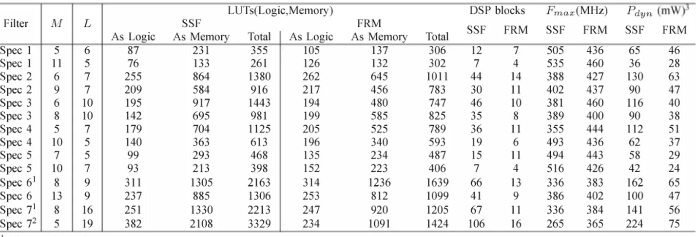
V. RESULTS
This section presents the results. The designs are implemented on Xilinx Virtex--6 VLX75T, speed grade -2. For all these results seven filter specifications, as adapted from [4], [12], are given by Table II. The passband and stopband ripples are
0.001
and0.0001
respectively for all specifications.TABLE II
FILTER SPECIFICATIONS CONSIDERED [4], [12].
Filter specification Spec 1 Spec 2 Spec 3 Spec 4
Passband edge (rad) O.057r O.097r O.Oh O.04047r Stopband edge (rad) O.h O.h O.027r O.05567r
Filter specification Spec 5 Spec 6 Spec 7
Passband edge (rad) O.OOh O.0457r O.0157r Stopband edge (rad) O.0257r O.057r O.027r
The design method for all these filters is simple. Matlab's firpm was used to design all the filters. Optimization of the filters is possible using advance techniques which could further reduce the filters' complexity.
A. Effect of Time-Multiplexing
The complexity using FRM initially decreases as the period L is increased. In this context, complexity can either mean the number
(a) (b) 60 14 c ---+--Single stage 12 .
�
50 Periodic model � :a 40 --+--Masking'g.
10 ." --TotalFRM]
�
30 � � 0b
20 � � � E E 10 �----i
z 2 0 0 3 6 3 6 Period, L Period, L (c) (d) � � 8 :a 8:g.
6 ."�
6 � E '0�
4 " 4 � � E�
2i
2 0 0 3 3 Period, L Period, LFig. 4. Number of multipliers for spec. I and M = (a) 1 (b) 5 (c) 6 (d) 8.
of multiplications
(M
=1)
or multipliers(M
>1),
as given byTable I.
However, there is an optimal point, beyond which increasing L increases the overall complexity of the filter. This is because as the model filter becomes more sparse, the masking filter length increases. This is illustrated in Fig. 4(a). This optimal point is dependent on the time-multiplexing factor, as shown in Fig. 4(c-d), where the optimal point in terms of number of multiplications at L = 5 in Fig. 4(a) is
now at L = 4,6, L = 5 and L = 4 for
M
= 5, 6, 8 respectively.Also shown in Fig. 4 is that the complexity of FRM can even go beyond that of the single stage filter.
This dependency on time-multiplexing is further highlighted by looking at the values of L at which complexity is minimum as
M
varies. This is shown in Fig. 5 for specifications 3 and 5. It is clear that there is no single optimal period L and that it depends on the time-multiplexing factorM.
(a) 20 ** **** *** * ** I; * * ** * * * *** * *** *** -0 * * * ** **�"
10 *** ** **** ***** * * ******* ***** *** *** ***** **** ci' * ** ** 0 0 ; 10 I; 20 Time-nlUltiplexing factor,M I; 10 -0�"
ci' 0 0 (b) * **** * ** * ** ****** *** ** **** **** **** ******* * * *** ***** * * ** 5 10 15 20 Time-multiplexing factor,MFig. 5. Points of minimum complexity for spec. 3 (a) and spec. 5 (b).
B.
Performance Matrix for the Implemented Filter
The results of resource utilization, maximum frequency and power consumption are shown in Table III. The values of
M
and L are picked based on the values at which we get the minimum number of multipliers. All the designs are placed and routed and static timing analysis is run on the routed design. In almost all the cases, FRM achieves lower complexity as compared to the SSF. Due to sometimes high DSP count, SSF cores for three specifications are implemented on larger FPGAs from the same family as shown in Table III. The results are still comparable.TABLE III PERFORMANCE MATRIX
L UTs(Logic,Memory) DSP blocks Fmax(MHz) Pdyn (mWY
Filter M L SSF FRM SSF FRM SSF FRM SSF FRM
As Logic As Memory Total As Logic As Memory Total
Spec 1 5 6 Spec 1 11 5 Spec 2 6 7 Spec 2 9 7 Spec 3 6 10 Spec 3 8 10 Spec 4 5 7 Spec 4 10 5 Spec 5 7 5 Spec 5 10 7 Spec 61 8 9 Spec 6 13 9 Spec 71 8 16 Spec 72 5 19 1 Virtex-6 VLX130T 2 Virtex-6 VLX550T 3 Pdyn@100MHz 87 76 255 209 195 142 179 140 99 93 311 237 251 382 231 355 105 133 261 126 864 1380 262 584 916 217 917 1443 194 695 981 199 704 1125 205 363 613 196 293 468 135 213 398 152 1305 2163 314 885 1306 253 1330 2213 247 2108 3329 234
One of the major contributors towards the lower LUT count for FRM is the better utilization of distributed memories. In Virtex-6, one can implement 32, 64 and 128-bits memory. 32 and 64-bit dual port memories occupy two LUTs and a 128-bit memory occupies four LUTs. For non-sparse filters, the depth of memories is equal to M. Only for a value of M = 32 or 64 or 128, the whole memory is fully utilized. On the other hand, since we only store non-zero coefficients to implement the periodic model filter, it not only decreases the total number of data memories, it also increases the depth of each memory, thus having a better utilization of the resources as shown in Fig. 6 for specification number 7. Fig. 6(a) shows the total memory bits required for each filter's data memories and Fig. 6(b) shows the total number of LUTs. It is evident, that although the total number of memory bits required by FRM is larger, the total number of LUTs is quite less. The jumps observed between L = 6 and 7 and L = 12 and 13 is due to the transition between one type of memory to the other type. The same trend is observed for all filter specifications and various values of M and L. This is one major advantage of implementing FRM on FPGAs which leads to fewer LUTs for data memories despite more delay elements initially.
2.5 x 10' (a) ... ,-��-����-.... -. 5 1 5 o o � Single stage -- Periodic model _____ Masking -+-TotalFRM 10 15 Period, L .-20 (b) 4000 3000
§
2000 ,.J 1000 0 0 10 15 Period, L Fig. 6. Data memory bits and LUTs for Spec. 7, M = 10.20
The lower complexity of FRM filters translate directly to lower power consumption as shown in Table III. The power numbers are obtained by simulating the post place and route simulation model at a clock frequency of 100 MHz for 1000 input data words and generating value change dump (vcd) file. Only dynamic power is considered in the last two columns because quiescent (static) power is more or less constant for a particular FPGA.
137 306 12 7 505 436 65 46 132 302 7 4 535 460 36 28 645 1011 44 14 388 427 130 63 456 783 30 11 402 437 90 47 480 747 46 10 381 460 116 40 585 825 35 8 389 400 90 38 525 789 36 11 355 444 112 51 340 593 19 6 493 436 62 37 234 487 15 II 494 443 58 29 223 406 7 4 516 426 42 24 1236 1639 66 13 336 383 162 65 812 1099 41 9 386 402 100 47 920 1205 67 II 336 384 141 56 1091 1424 106 16 265 365 224 75 VI. CONCLUSION
In this paper, we presented a low power FIR filter architecture for narrow transition bands using FRM techniques. This low power consumption is achieved because of lower resource utilization. We also pointed out that better memory utilization by the FRM filters is one of the reasons behind reduced power consumption. Furthermore, we presented that the optimal point in terms of low complexity for FRMfilters differs with changes in M. Although the presented architecture is only for narrow band fi lters, they can be easi ly employed to implement wide band filters by using the same memories present.
REFERENCES
[I] S. K. Mitra, Digital Signal Processing. University of California, Santa Barbara: TATA McGraw-Hill, 2006.
[2] Y-C. Lim, "Frequency-response masking approach for the synthesis of sharp linear phase digital filters," iEEE Trans. Circuits Syst., vol. 33, no. 4, pp. 357-364, 1996.
[3] T. Saramiiki, "Finite impulse response filter design," in Handbook for
Digital Signal Processing, S. K. Mitra and J. Kaiser, Eds.
Wiley-Interscience, 1988, pp. 155-277.
[4] T. Saramiiki, T. Neuvo, and S. K. Mitra, "Design of computationally efficient interpolated FIR filters," iEEE Trans. Circuits Syst., vol. 35, no. I, pp. 70-88, 1998.
[5] Y Lian, "FPGA implementation of high speed multiplierless frequency response masking FIR filters," in Proc. iEEE Workshop Signal Process ing Syst., Lafayette, LA, 2000, pp. 317-325.
[6] Y C. Lim, Y J. Yu, H. Q. Zheng, and S. W. Foo, "FPGA implementation of digital filters synthesized using the frequency-response masking technique," in Proc. JEEE into Symp. Circuits Syst., vol. 2, Sydney, NSW, May 2001, pp. 173-176.
[7] S. Li and J. Zhang, "Efficient FPGA implementation of sharp FIR filters using the FRM technique," iEICE Electronics Express, vol. 6, no. 23, pp. 1656-1662, Dec. 2009.
[8] S. G. Patronis and L. S. DeBrunner, "Sparse FIR filters and the impact on FPGA area usage," in Proc. Asilomar Con! Signals Syst. Comput., Pacific Grove, CA, Oct. 2008, pp. 1862-1866.
[9] S. A. Alam and O. Gustafsson, "Implementation of time-multiplexed sparse periodic FIR filters for FRM on FPGAs," in Proc. iEEE Int. Symp. Circuits Syst., Rio de Janeiro, Brazil, May 2011.
[10] Xilinx, Virtex-6 FPGA DSP48Ei Slice User GUide, Sep. 2009. [Online]. Available: http://www.xilinx.com/support/documentation/virtex-6.htm [II] --, FIR LogiCORE IP FIR Compiler v5.0, 2009. [Online]. Available:
http://www.xilinx.comlsupport/documentation/ipdsp_filter.htm [12] Y Neuvo, D. Cheng-Yu, and S. Mitra, "Interpolated finite impulse
response filters," IEEE Trans. Acoust., Speech, Signal Process., vol. 32, pp. 563-570, May 1984.
![Fig. 2. Pipelined time-multiplexed architecture for periodic model filters [9]](https://thumb-eu.123doks.com/thumbv2/5dokorg/5500375.143245/3.918.494.805.347.606/fig-pipelined-time-multiplexed-architecture-periodic-model-filters.webp)
![Fig. 3. Time-multiplexed architecture using the final accumulator DSP block for the middle tap [9]](https://thumb-eu.123doks.com/thumbv2/5dokorg/5500375.143245/4.918.97.424.77.339/time-multiplexed-architecture-using-final-accumulator-block-middle.webp)