Department of Physics, Chemistry & Biology
Master’s Thesis
Design and Characterization of a Synchronous
Co-axial Double Magnetron Sputtering System
Asim Aijaz
LiTH-IFM-A-EX-09/2041-SE
Department of Physics, Chemistry & Biology Linköping University, SE-581 83 Linköping, Sweden
i
Department of Physics, Chemistry & Biology
Master’s Thesis
Design and Characterization of A Synchronous
Co-axial Double Magnetron Sputtering System
Asim Aijaz
LiTH-IFM-A-EX-09/2041-SE
Department of Physics, Chemistry & Biology Linköping University, SE-581 83 Linköping, Sweden
iii Nyckelord
Keyword: HiPIMS, magnetron sputtering, co-axial double magnetron, side-ways deposition, cylindrical
shaped objects.
Sammanfattning Abstract
High power impulse magnetron sputtering (HiPIMS) is a novel pulsed power technique. In HiPIMS, high power pulses are applied to the target for short duration with a low duty factor. It provides a high degree of ionization of the sputtered material (in some cases up to 90%) and a high plasma density (1019 m-3) which results in densification of the grown films. Recently a large side-transport of the sputtered material has been discovered, meaning that the sputtered material is transported radially outwards, parallel to the cathode surface. In this research, we use this effect and study the side-ways deposition of thin films. We designed a new magnetron sputtering system, consisting of two opposing magnetrons with similar polarity. Ti films were grown on Si using the side-ways transport of sputtered material. Scanning electron microscope was employed to investigate the microstructure of the grown films. Optical emission spectroscopy (OES) measurements were made for investigating the ionized fraction of the sputtered material while Langmuir probe measurements were made for evaluating the plasma parameters such as electron density. The conclusion is that the system works well for side-ways deposition and it can be useful for coating the interior of cylindrically shaped objects. It is a promising technique that should be used in industry.
Datum
Date: 2009-01-27
Avdelning, institution
Division, Department
Department of Physics, Chemistry and Biology, IFM Linköping University, SE-581 83,Linköping, Sweden
URL för elektronisk version http://www.ep.liu.se/
ISBN
ISRN: LITH-IFM-A-EX--09/2041--SE
_________________________________________________________________
Serietitel och serienummer ISSN
Title of series, numbering ______________________________
Språk Language Svenska/Swedish Engelska/English English Rapporttyp Report category Licentiatavhandling Examensarbete C-uppsats D-uppsats Övrig rapport _____________ Titel
Title: Design and Characterization of A Synchronous Co-axial Double Magnetron Sputtering System
Författare
Author: Asim Aijaz
Nyckelord
Keyword: HiPIMS, magnetron sputtering, co-axial double magnetron, side-ways deposition, cylindrical
shaped objects.
Sammanfattning Abstract
High power impulse magnetron sputtering (HiPIMS) is a novel pulsed power technique. In HiPIMS, high power pulses are applied to the target for short duration with a low duty factor. It provides a high degree of ionization of the sputtered material (in some cases up to 90%) and a high plasma density (1019 m-3) which results in densification of the grown films. Recently a large side-transport of the sputtered material has been discovered, meaning that the sputtered material is transported radially outwards, parallel to the cathode surface. In this research, we use this effect and study the side-ways deposition of thin films. We designed a new magnetron sputtering system, consisting of two opposing magnetrons with similar polarity. Ti films were grown on Si using the side-ways transport of sputtered material. Scanning electron microscope was employed to investigate the microstructure of the grown films. Optical emission spectroscopy (OES) measurements were made for investigating the ionized fraction of the sputtered material while Langmuir probe measurements were made for evaluating the plasma parameters such as electron density. The conclusion is that the system works well for side-ways deposition and it can be useful for coating the interior of cylindrically shaped objects. It is a promising technique that should be used in industry.
v
Abstract
High power impulse magnetron sputtering (HiPIMS) is a novel pulsed power technique. In HiPIMS, high power pulses are applied to the target for short duration with a low duty factor. It provides a high degree of ionization of the sputtered material (in some cases up to 90%) and a high plasma density (1019 m-3) which results in densification of the grown films. Recently a large side-transport of the sputtered material has been discovered, meaning that the sputtered material is transported radially outwards, parallel to the cathode surface. In this research, we use this effect and study the side-ways deposition of thin films. We designed a new magnetron sputtering system, consisting of two opposing magnetrons with similar polarity. Ti films were grown on Si using the side-ways transport of the sputtered material. Scanning electron microscope was employed to investigate the microstructure of the grown films. Optical emission spectroscopy (OES) measurements were made for investigating the ionized fraction of the sputtered material while Langmuir probe measurements were made for evaluating the plasma parameters such as electron density. The conclusion is that the system works well for side-ways deposition and it can be useful for coating the interior of cylindrically shaped objects. It is a promising technique that should be used in industry.
vii
Acknowledgements
First of all I like to thank Almighty Allah, Who is the real source of knowledge and wisdom and without His help and blessings, nothing is possible.
Furthermore, I take this opportunity to show my gratitude towards all those people who helped me during this diploma work, making it a valuable experience.
I like to thank….
Prof. Ulf Helmersson, for giving me the opportunity to do this work under his supervision, for providing good ideas, for being ready all the time to discuss problems. You always remain polite and put your trust in your students and that works….Thank you Ulf.
Daniel Lundin, for being a wonderful supervisor, for providing me all sorts of help whenever I got stuck anywhere during this work, for showing patience while answering my questions, for taking his time out whenever I needed it from a very busy schedule and heavy work load. You boosted my confidence and showed me how research is performed with a good planning.
Petter Larsson, for being an amazing person when it comes to solving technical problems. You play a big role in the good research that is performed in the Plasma & Coatings Physics division.
Montri Aiempanakit and Daniel Magnfält, for providing a good office environment and for non-work related discussions that we had during this time. I enjoyed your company.
viii
All other members of the Plasma & Coatings Physics Division, for making it a wonderful place to work.
Special thanks to Leif Johansson, my master’s program co-ordinator, for providing a valuable guidance and support throughout my master’s studies, for being available to solve minor and major problems. Your encouragement and support helped me in early completion of my MS.
All my friends in Linköping, for making me feel at home away from home. It is a great pleasure to have all of you in my life.
My mother, the most precious asset of my life, who prays for my success day and night. I can never forget how hard you worked for providing me the means of getting an education.
All other family members of mine, for supporting me whatever I do in my life. I love you all and I am nothing without you.
Asim Aijaz Linköping, January 2009
ix
Contents
1 Introduction
11.1 Background . ……… 1
1.2 Aim of the thesis ………. 2
1.3 Outline ………. 3
2 Thin film growth and deposition techniques
52.1 Overview ………. 5
2.2 Plasma and its role in thin film deposition ... 7
2.3 Sputtering process and surface interactions ……… 9
2.4 Magnetron sputtering ... 10
2.4.1 Direct current magnetron sputtering (dcMS) ……… 14
2.4.2 High power impulse magnetron sputtering (HiPIMS) ………….. 15
3 Experimental details
17 3.1 Design of the synchronous co-axial double magnetron sputtering system ……….. 173.2 Thin film analysis ……… 20
3.2.1 Scanning electron microscopy (SEM) ………... 21
3.3 Plasma analysis ……… 23
3.3.1 Optical emission spectroscopy (OES) measurements …………... 23
3.3.2 Langmuir probe measurements ………. 25
3.3.2.1 Langmuir probe theory and evaluation of plasma parameters ……… 27
3.3.2.2 Experimental setup for Langmuir probe measurements ……….. 30
x
4 Results
33 4.1 Film Analysis ……….... 33 4.1.1 Microstructural analysis ……….………. 33 4.1.1.1 dcMS films ………... 33 4.1.1.2 HiPIMS films ……….... 374.1.2 Deposition rates of the film growth ..………... 42
4.1.2.1 Comparison of deposition rates at different distances between the magnetrons for dcMS ………... 42
4.1.2.2 Comparison of deposition rates at different distances between the magnetrons for HiPIMS ………..…. 43
4.1.2.3 Comparison of deposition rates at different Ar gas pressures for HiPIMS ………... 44
4.2 Plasma analysis ……… 45
4.2.1 Optical emission spectroscopy measurements for dcMS and HiPIMS plasmas ………. 45
4.2.2 Langmuir probe measurements (LPM) ………... 49
4.2.2.1 For dcMS plasma ..………... 49
4.2.2.2 For HiPIMS plasma .,,,,,,,,.………... 53
5 Discussion
576 Conclusions
637 Future Outlook
65References
671
1 Introduction
1.1 Background
Thin film technology is simultaneously one of the oldest arts and one of the latest sciences [1]. The Egyptians are believed to be the earliest craftsmen in this field by producing a decorative gold leaf by gliding, which dates back to the eighteenth dynasty (1567-1320 B.C). The leaf measured about 0.3 micron in thickness [2]. Since then thin film science has taken a huge leap in becoming one of today’s vital technologies, having a big impact on a large variety of industrial applications. These applications involve decorative, wear and corrosion resistant coatings, optical and magnetic thin films, thin film solar cells, thin film electro-acoustic devices and porous nanocomposite films to name just a few. Generally, the term thin film is applied to layers which have thicknesses on the order of microns or less and may be as thin as a few atomic layers. On the other hand, the thicker layers of films are usually called “coatings”. The idea behind thin film deposition is that these films are deposited onto bulk materials to acquire the properties which may not be obtained in bulk alone [3]. Additional functionality in the films can be achieved by depositing multiple layers of different materials such as TiN coatings on cutting tools simultaneously providing hardness and low friction.
The increasing applications of thin films and coatings have been leading material scientists and material processing engineers to focus not only on the study of new and multi-functional materials but also motivating them to develop new deposition systems to broaden the spectrum of applications. At present, various thin film deposition systems employing different operating principles, configurations and component geometries are in use sufficing the need for the growth of metal, oxide and
2
alloy films etc. Magnetron sputtering and its variants represent one class of such systems (see sec. 2.4). A fundamental step towards the improvement of the magnetron sputtering technique was the introduction of an unbalanced magnetron (see sec. 2.4), provided by Window and Savvides in 1986 [4]. The study of the unbalanced magnetron continued giving improved versions of this configuration and leading to the development of multi-cathode unbalanced magnetron sputtering systems. Sproul et al. developed a dual cathode, high rate reactive sputtering system [4]. They made studies onto different magnetic field configurations in a dual cathode arrangement, referred to as close field and open field (mirrored) magnetron configurations. Both of these configurations will be discussed in more detail in sec. 2.4. These multi-cathode magnetron sputtering systems provide the enhancement in sputtering rates and ionization conditions specially when operated with a pulsed power. Today, many of the improved forms of multi-cathode magnetron sputtering systems have been developed and are used within industry [5]. These systems make use of only the closed field configuration. Open field or mirrored multi-cathode magnetron sputtering systems have not attracted researchers’ attention to any greater degree. The reason behind this is that the sputtered ions get transported sideways (parallel to the surface of magnetrons). This results in a decrease in the plasma density in a region between the two opposing magnetrons where a substrate is usually placed. Recently Lundin et al., discovered a cross-field ion transport in a single unbalanced magnetron sputtering system operated with a relatively newly developed pulsed power sputtering technique called high power impulse magnetron sputtering (HiPIMS) [6]. This discovery may provide means of making the sideways deposition of thin films possible especially when this concept is employed in an open field multi-cathode sputtering system. The research work presented in this thesis is an attempt to contribute to the development of multi-cathode magnetron sputtering systems with mirrored or open field configuration, in particular operating with a pulsed power.
1.2 Aim of the Thesis
The aim of this research is to develop a multi-cathode magnetron sputtering system with an open field configuration which can be utilized to make sideways depositions of thin films. The implementation of the idea of this system was carried out by mounting two circular magnetrons facing each other co-axially and operating
3
synchronously in a conventional cylindrical vacuum chamber. This “Synchronous Co-axial Double Magnetron Sputtering System” operating with direct current magnetron sputtering (dcMS) and HiPIMS modes was used for depositing Ti coatings on Si substrates and studying the properties of the plasma associated with this new sputtering system. Scanning electron microscopy (SEM) was employed to measure the thickness and to investigate the uniformity of the grown films. Optical emission spectroscopy (OES) measurements were made for the determination of ionized fraction of the sputtered material. Langmuir probe measurements (LPM) were made for studying the plasma properties and subsequently determining the plasma parameters such as plasma potential, floating potential, electron density, electron energy distribution function and effective electron temperature etc. The sputtering parameters that have been varied for these measurements were the distance between the two magnetrons as well as the working gas pressure. The motivation behind using the techniques of dcMS and HiPIMS for all of the above mentioned measurements, has been to compare the two techniques as well as making this new sputtering system an attractive option for thin film growth on an industrial scale. The details of the design and operation of this “Synchronous Co-axial Double Magnetron Sputtering System” are presented in section 3.1.
1.3 Outline
This thesis is structured as follows. Chapter 2 contains the description about the role of a plasma in thin film growth processes and the description of different magnetron sputtering techniques used in this work. In chapter 3, all the experimental details are provided, including a thorough breakdown of the new sputtering system design. The experimental results are presented in chapter 4 and the discussion on these results is made in chapter 5. In chapter 6 this research work is concluded. Finally chapter 7 gives the future outlook of this research.
5
2 Thin Film Growth and Deposition
Techniques
2.1 Overview
In order to understand various aspects of this work it is of essence to look into the fundamentals of a thin film deposition process in a bit more detail. There exist various processes for growing thin films and coatings. In general, all thin film processes comprise of four or five steps that are described as follows. The source of material to be deposited as a thin film, which is usually called a target is provided. The source material may be in the form of a solid, liquid or gas. This material is transported to an object to be coated, which is called a substrate. The deposition takes place and the resulting film may be annealed before it is analysed [7]. Analysis of the film after the deposition can be regarded as the final stage of the film formation process. It may involve the direct measurement of the desired and important properties of the film such as the hardness of the film used for a cutting tool, the break down voltage of an insulating film or the transparency of an optical film.
Depending on the type of source material and means of transporting this material to a substrate, a thin film process can be regarded as electroplating, chemical vapor deposition (CVD) or physical vapor deposition (PVD). Electroplating is one of the most simple and commonly used forms of thin film deposition. In this, an object is coated by immersing it into a solution such as an acid containing a dissolved metal. A coating is formed on the surface of the object through attracting positive metal ions by applying a negative charge on it. The other widely used process is chemical vapor deposition (CVD), in which a material to be deposited is in a volatile compound form
6
and reacts with the other gases to produce a nonvolatile solid that is subsequently deposited on a suitable substrate atomistically. Another common thin film process is the physical vapor deposition (PVD). This is an atomistic deposition process in which a material is vaporized from a solid or a liquid source in the form of atoms or molecules. The evaporated material gets transported in a low pressure or a plasma environment to a substrate where it condenses and forms thin layers of films. The primary source of energy may be electrons, photons or ions which, apart from vaporizing the source material play an important role in activating the atoms during their transport or modifying the film structure during deposition [8]. Commonly used thin film deposition techniques such as the thermal evaporation, arc evaporation, laser ablation and sputtering etc., stand under the banner of PVD. Each of these techniques is briefly described here.
In a process of thermal evaporation, thermal energy is imparted to atoms in a liquid or a solid source. This causes their temperature to be raised to a level where the atoms may efficiently evaporate or sublime. Subsequently they transfer themselves to a substrate located at some distance from the source, where the film formation proceeds atomistically. The other common technique is arc evaporation, in which a high current and a low voltage arc is produced on the surface of a target in a small area (cathode spot) causing an ejection of the target material. The ejected material condenses on the substrate and subsequent film formation takes place. Another process of film formation is laser ablation in which laser radiation interacts with a solid target. Absorption of energy and localized heating of the target surface causes the material from the target to be vaporized, which is deposited on the substrate and hence film formation occurs. The final PVD technique which is described here resembles deposition method like evaporation and it is called sputtering. Sputtering differs from the evaporation in that gaseous ions impinge on the source surface which is maintained usually at room temperature. These ions eject the atoms from the source through momentum transfer and thereby cause the source material to be deposited on the substrate. A modified form of sputtering is called magnetron sputtering, which has become a widely spread technique in modern thin film technology. This technique along with its variants will be described in sec. 2.4. Furthermore, it can be inferred from the discussion made above regarding all of the PVD processes that these processes exploit the formation of vapors from a solid or a liquid phase for the thin
7
film formation. Also the method used to form the vapor defines the characteristics of vapor atoms, such as their energy distribution, velocity distribution, flux of atoms and their degree of ionization etc. In addition, these above mentioned characteristics of vapor atoms can also be influenced by electrons, ions, or photons (see sec. 2.2). When a PVD process contains a plasma environment it is called plasma-based PVD. The work presented in this thesis is based on a plasma-based PVD process therefore it is important to understand the fundamentals of a plasma and the role it plays in thin film growth.
2.2 Plasma and Its Role in Thin Film Growth
In general, plasma may be defined as a quasi neutral gas that exhibits a collective behavior in presence of electromagnetic fields. It consists of electrons, ions and neutral atomic and molecular species. The term plasma was first used by Irvin Langmuir in 1929 [9]. Plasma is also said to be the fourth state of matter and it plays an imperative role in material processing, particularly in PVD, where it is confined within an evacuated vacuum chamber. Inside the chamber, there are generally two electrodes, one of which is the target of the material to be deposited and it is connected to the negative terminal of the power supply hence it serves as cathode. The other electrode, the anode, is usually the grounded chamber walls. Opposite to the cathode is a substrate which may be grounded, biased positively or negatively, heated or cooled. The chamber is evacuated and an inert gas such as argon is introduced and a pressure within the range of a few to a hundred of millitorr is maintained. By applying a voltage to the cathode an electric discharge is initiated and sustained where the gas serves as a medium for this discharge. Afterwards, a current flows when a visible glow discharge, a plasma, is maintained between the two electrodes.In order to understand the behavior of the conduction via plasma on a microscopic scale, the mechanism responsible for this phenomenon should first be considered. This process starts with a free electron, present for example due to cosmic radiation or thermal energy, which is accelerated by the electric field towards the anode. While travelling, the electron may gain sufficient energy and collide with a neutral gas atom and subsequently ionize it. Due to this impact ionization, the following reaction takes place, which ejects two electrons further:
8 Ar e Ar e o 2
These ejected electrons are accelerated due to presence of the electric field and interact with two neutral gas atoms, releasing more ions and electrons. The ions move in the opposite direction to the electric field and impinge on the cathode ejecting, among other particles, secondary electrons. This regime is called the Townsend discharge and a small current flows in the system due to a small number of charge carriers.
Figure 2.1. Different plasma discharge regimes [10].
The secondary electrons undergo charge multiplication which leads to a rise of the current effectively indicating the breakdown of the neutral gas. Now the gas begins to glow and the voltage drops which is accompanied by a sharp increase of the current. This is known as the normal glow regime. In this case the ion bombardment increasingly spreads over the cathode surface with increment in power until a uniform current density is achieved. The discharge is driven into the abnormal discharge regime with further increase in the power resulting in the higher voltage and cathode current-density levels. The processes such as sputtering or plasma etching are operated in this realm. Further increase of the power causes the thermionically emitted
9
electrons to be exceeded to that of secondary-electron emission propagating the low-voltage arcs. This is the arc discharge regime and is utilized in the cathodic arc deposition process.
The discussion made above provides a clear picture of how a plasma behaves with respect to the applied power. This behavior of the plasma over a wide range of the applied power was divided into different discharge regimes (See figure 2.1). In this work, the process of sputtering is the main concern, and therefore a description of the interaction between plasma species and surface of the target within the abnormal glow discharge regime is made with a bit of re-introduction of the phenomena of sputtering in the next section.
2.3 Sputtering Process and Surface Interactions
Sputtering refers to the phenomenon of ejection of particles such as atoms or molecules from the surface of a material in response to impinging species such as ions from an ion-beam or a plasma. These ions, directed towards the cathode under the influence of an electric field created by a potential difference between the cathode and the anode, strike and erode the target (cathode) material. As a result, there occurs an ejection of the individual atoms, group of atoms or molecules via the momentum transfer. This ion-surface interaction does not always result in sputtering, and depending on the energy of the incoming ions, they may also reflect back, stick or adsorb, scatter or get buried in surface layers. Moreover, the ejected species are not only comprised of charged particles (electrons, ions), but also neutrals and photons of varying energies and abundance may be emitted from the surface.In the case of sputtering, three different ion-surface interaction schemes are possible as shown in figure 2.2 which involve a) single knock-on (low energy), b) linear collision cascade and c) spike (high energy). These three energy regimes of sputtering can be summarized as higher energy of the impinging ions causes more collisions, which results in more sputtered atoms. The basic sputtering process as described above is limited by low deposition rates, a low ionization efficiency and high substrate heating effects [12]. The origin of the slow rate of sputtering is intimately tied to a very low efficiency in the use of electrons to create ions. The problem of low ionization of the sputtering gas at a given pressure can be overcome by injecting more
10
electrons by some means, for example by thermionic emission from an independent electrode.
Figure 2.2. Energy regimes of sputtering: a) Single knock-on (low energy), b) Linear cascade, and c) Spike (high energy) [11].
A better solution of the low ionization problem was presented in 1930 by Penning [13] with his invention of the magnetron. The importance of using this magnetron in connection with sputtering, and the remarkable benefits it provides in order to overcome the problems encountered with simple sputtering as described above, are discussed in the next section.
2.4 Magnetron Sputtering
Magnetrons make use of the fact that a magnetic field configuration parallel to the target surface can confine the motion of secondary electrons ejected by the bombarding ions, to a close vicinity of the target surface as shown in figure 2.3. An array of permanent magnets is placed behind the sputtering source. In the case of circular magnetrons, the magnets are placed in such a way that one pole is positioned at the central axis of the target, and the second pole is placed in a ring around the outer edge of the target.
This configuration creates crossed E and B fields, where electrons drift perpendicular to both E and B according tovEB/ B2. If the magnets are arranged in such a way that they create closed drift regions, then the electrons are trapped, move in a spiral
11
path and rely on collisions to escape (or other type of slightly more complicated diffusion mechanisms).
Figure 2.3. A schematic showing the principle of a magnetron [14].
These trapped electrons suffer more collisions, due to their constrained motion, with the neutral sputtering gas atoms near the target surface. This increases the net density of ions and electrons in the plasma. The increase in the density of ions of sputtering gas leads to an increased ion bombardment on the target, giving higher sputtering rates and therefore higher deposition rates at the substrate are achieved. The electron confinement also allows for a magnetron to be operated at much lower voltages compared to basic sputtering (approx. 500 V instead of 2-3 kV) and can be used at lower pressures typically in the mTorr region [15]. This is an advantage since less material is lost to the chamber wall and back to the target through scattering in the discharge gas.
A disadvantage of using a magnetic field is that the shape of the magnetic field efficiently erodes the target where the magnetic field lines are parallel to the target surface; a so-called race track is created. The major drawback of these early magnetrons was the too good confinement of dense plasma near the surface of the target. The reason behind this confinement near the surface is that these magnetrons, called intermediate or balanced magnetrons, use equally strong magnets at the central axis and around the outer edge of the target. It means that the magnetic field lines emerging and reentering into the target form closed loops. Since the motion of electrons is confined to these closed loops the ionization increases only near the target
12
surface where these electrons make collisions with the sputtering gas atoms. Therefore the plasma available further away at the substrate has very low density to activate reactive gases and the ion bombardment for modification of the growing film is suppressed. This problem can be overcome by unbalancing magnetrons by strengthening the magnetic pole in the middle resulting in an opening up of closed magnetic field lines. In this way, a larger portion of the secondary electrons can escape from the near cathode region, thus increasing the plasma density at the substrate compared to the case of a balanced magnetron. As a result, ion bombardment at the substrate increases which provides an improvement in the coating structure. The concept of an unbalanced magnetron was first developed by Window and Savvides, who investigated the effect of varying the magnetic field configuration of a balanced magnetron [16]. There are two types of unbalanced magnetrons. Type I in which the magnetic pole in the middle of the magnetron is strengthened compared to the pole at edges. Type II in which the magnetic pole at the edges is strengthened compared to the pole in the middle. The schematic of all three types of the magnetrons is shown in figure 2.4.
Figure 2.4. Simple cross-sectional schematic of a circular magnetron showing the magnetic field lines for the different kinds of magnetron configurations [17].
The magnetic field configuration that is utilized in unbalancing the magnetrons implies that high ion current can be transported to the substrate. However, a disadvantage of the unbalanced magnetrons is that the flux of the escaping electrons is not uniform, and thus the generated plasma is non-uniform [18]. In order to utilize the
13
advantages of the unbalanced magnetron configuration as well as overcoming the problem of a non-uniform plasma, Sproul et al. studied and developed multiple unbalanced magnetron sputtering systems [19, 20] as shown in figure 2.5. The system in which two unbalanced magnetrons are installed opposite to each other and configured with the opposite magnets of the same polarity is called a mirrored unbalanced magnetron sputtering system. The one employing two opposing unbalanced magnetrons and configured with the opposite magnets of the opposite polarity is called a closed field unbalanced magnetron sputtering system. In the mirrored unbalanced magnetron sputtering system the field lines are directed towards the chamber walls. Secondary electrons following these magnetic lines are lost to the chamber walls resulting in a low plasma density in the region between the two magnetrons. Conversely, in the closed field unbalanced magnetron sputtering system, the magnetic fields lines emerging out of the opposing magnetrons form closed loops, reducing the losses of secondary electrons to the chamber walls. Therefore, a high density plasma is maintained in the region between the two magnetrons. Several variants of the closed field unbalanced magnetron configuration have been developed for specific applications [12].
(a) (b)
Figure 2.5. Schematic showing (a) an open or mirrored (b) a closed field unbalanced magnetron configuration [4].
14
From the description of the multiple unbalanced magnetrons it can be inferred that the concept of the mirrored unbalanced magnetron configuration can be utilized for sideways depositions of the film where the substrate to be coated is placed sideways and perpendicular to the surface of both opposing magnetrons. This concept was used for the designing of a new magnetron sputtering system in this work. The details of this design are presented in section 3.1. Moreover, the newly designed magnetron sputtering system was operated with two variants of magnetron sputtering namely direct current magnetron sputtering (dcMS) and high power impulse magnetron sputtering (HiPIMS) which will be discussed in the next section. As mentioned in section 1.2, both of these techniques have been used for all measurements in this work with the motivation of comparison of results.
2.4.1 Direct Current Magnetron Sputtering (dcMS)
In direct current magnetron sputtering (dcMS) a constant voltage is applied between the cathode and the anode. This is one of the simplest sputtering configurations and is used for the sputtering of conducting materials and reactive sputtering of compounds (by the use of a reactive gas such as N2 or O2). This technique has the limitation for electrically insulating targets, where current no longer can be drawn. The plasma density resulting from the power dissipated in a conventional dcMS plasma is on the order of 1017 m-3 in a close vicinity of the target with typical average electron energy of the order of a few electron volts (eV) [21]. A low plasma density results in a low degree of ionization of the sputtered material, typically a few percent [21]. A high degree of ionization is desired in order to obtain a dense microstructure of the grown films since the ionized species can be guided by electric and magnetic fields. The problem of a low degree of ionization can partially be solved by delivering a higher power to the target resulting in a higher sputter yield and a denser plasma, which in turn provides a high degree of ionization. However, one limitation is encountered in this case; high applied power increases the heat load on the target and can eventually melt it. The typical cathode potentials in the dcMS case are in the range of 300 V to 700 V which leads to current densities below 100 mAcm-2, resulting in power densities upto 50 Wcm-2 [22]. These problems can be overcome by employing a new
15
sputtering technique called high power impulse magnetron sputtering (HiPIMS) which will be discussed in the following section.
2.4.2 High Power Impulse Magnetron Sputtering
(HiPIMS)
In order to acquire a high degree of ionization, PVD techniques have been developed where at least 50% of the deposition flux is ionized, so-called IPVD techniques [23]. The development of these PVD techniques was initially mainly driven by the need to deposit metal layers and diffusion barriers into trenches or vias of high aspect ratio, such as integrated circuits [24], but has during the past years found a number of additional areas where beneficial properties such as enhancing the substrate pre-treatment for improving adhesion of hard coatings are observed [23]. Cathodic arc evaporation and hollow cathode magnetron sputtering are such common IPVD techniques which have been utilized efficiently. A novel technique in this regard is high power impulse magnetron sputtering (HiPIMS) also known as high power pulsed magnetron sputtering (HPPMS) [23].
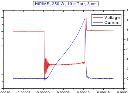
Figure 2.6. A HiPIMS voltage and current pulse.
While conventional magnetron sputtering discharges are characterized by a very low degree of ionization of the sputtered species, typically about 10% or lower, ionization of sputtered atoms can occur to a much greater extent in HIPIMS discharge [25]. It
-0.00010 -0.00005 0.00000 0.00005 0.00010 0.00015 0.00020 -800 -600 -400 -200 0 200 H iP IMS , 2 50 W , 1 0 m T orr, 3 cm Voltage C urrent T im e (sec) V o lt a g e ( v o lt s ) -20 0 20 40 60 80 100 120 140 C u rr e n t (a m p s )
16
utilizes high power pulses (peak discharge power density ~ 1000 Wcm-2) with a short duration to achieve high electron density plasma. A HiPIMS voltage and a current pulse recorded in this work are shown in figure 2.6. Plasma densities of the order of 1019 m-3 have been reported for HiPIMS [26] and several reports have shown highly ionized metal plasmas (see for example reference 21). The high density of the plasma leads to a high degree of ionization of the sputtered atoms (see figure 2.7) [27]. To ensure that the target has time to cool down between the pulses, the duty factor (ratio between pulse on time and total time) is kept low, usually around 1%. The ionization fraction reaches 30-70% but peak values of 90% have been reported for Ti [26].
Figure 2.7. Ionized flux fraction of the sputtered material as a function of the electron density as modelled by Hopwood [27].
The great advantage of the HiPIMS is that the technique is easy to apply on a conventional sputtering system and no troublesome rebuilding is required. The only modification is changing the power supply.
17
3 Experimental Details
3.1
Design of the Synchronous Co-axial Double
Magnetron Sputtering System
The experimental details for the magnetron sputtering system used for sideways deposition of thin films are presented here. The idea behind this concept is that a multi-cathode magnetron sputtering system is developed which provides such a magnetic field configuration which can be utilized for transporting the sputtered material flux sideways, that is, towards the walls of the sputtering chamber. This sideways transportation of the sputtered flux can be utilized for depositing thin films on substrates that are placed perpendicular to the surface of the target around the magnetrons. It may provide a good solution for coating complex shaped objects, such as the interior of cylindrically shaped objects by placing them around the magnetrons.
The side-ways transportation of the sputtered material is dependent on the plasma confinement. The plasma confinement is mainly dependent on the shape and behaviour of magnetic field lines originating from the magnetron and the greatest confinement of the plasma is in front of the magnetron. The plasma density outside this confinement region is substantially lower. For the case of a single magnetron, approximately three orders of magnitude lower density in the immediate vicinity of the rim of the magnetron has been reported [28].
One can now find an immediate solution to this low plasma density problem by making magnetic field lines extend to the region around the magnetrons. It will be much easier with an unbalanced magnetron because in this case the magnetic field lines also emerge vertically outward with respect to the surface of the magnetron. In
18
our system, we used two magnetrons therefore if another similar magnetron is mounted co-axially in such a way that both magnetrons face each other then the effect will be similar to that of two similar magnetic poles opposing each other. The field lines will drift towards the chamber walls and secondary electrons will follow these magnetic field lines. This will result in an increase in the plasma density around the magnetrons. This may be utilized for the sideways deposition of thin films. This configuration of a magnetic field in a multi-cathode unbalanced magnetron sputtering system is called the mirrored or the open field configuration.
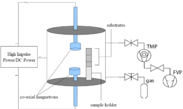
Figure 3.1. Schematic drawing of synchronous co-axial double magnetron sputtering system. The magnetrons are connected to a power supply. The substrates are mounted on a sample holder. A turbo molecular pump (TMP) and fore vacuum pump (FVP) are also connected to the chamber. A working gas (e.g. Ar) is let in through a gas inlet.
A schematic of the system is shown in figure 3.1. In this sputtering system two identical planar, circular, weakly unbalanced magnetrons each with 7 cm in total diameter equipped with a 5 cm diameter titanium (Ti) target (purity > 99.9 %) were mounted co-axially facing each other. They were placed inside cylindrically shaped vacuum system, 42 cm in diameter and height 30 cm, in such a way that one of the magnetrons was mounted in the lid facing vertically downward and the other was mounted into the base of the chamber facing vertically upward.
19
A static, grounded substrate holder having three 1.5 cm x 1.5 cm Silicon (Si) substrates mounted vertically in sequence was placed 2 cm away from the rim of the magnetron at ambient temperature. Prior to deposition, the substrates were ultrasonically cleaned in isopropanol for 10 minutes each. The center point of the
separation between the magnetrons was sought as the reference point for keeping track of deposition rates and uniformity of the grown films at various positions on the
substrates. The measurements were performed at various distances (3 cm, 4 cm, 5 cm and 8 cm) between the magnetrons to optimise the sputtering conditions in this new system while keeping the substrate holder at the same distance from the magnetrons. The vertical position of the substrate holder was adjusted for different distances between the magnetrons to make sure that all three substrates remain at a position such that the symmetry of different positions on the substrates is maintained with respect to the reference point. Before each measurement, the chamber was evacuated to a base pressure on the order of 10-6 Torr. In order to obtain the desired working gas pressure, an inert gas (Ar of purity 99.9997%) was introduced into the chamber through leak valves. All measurements were performed at ambient temperature with no substrate heating using either, dcMS or HiPIMS. For these measurements, both magnetrons were driven synchronously. In the case of dcMS the plasma was driven by a constant voltage MDX Pinnacle DC power supply (Advanced Energy). For HiPIMS the power was supplied by a SPIK 1000A pulsing unit (Melec) fed by the same DC power supply. Approximately square voltage pulses with specific width and repetition frequency are produced by this pulsing unit.
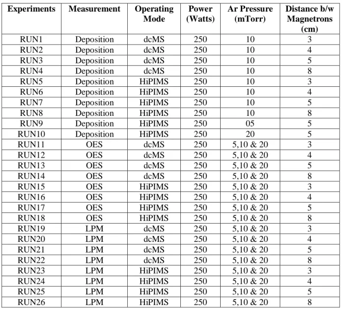
In this work, a total average power of 250 W was used for both the dcMS and the HiPIMS while the deposition time of 1 hour for the dcMS and 2 hours for the HiPIMS were chosen, due to a lower deposition rate in the case of HiPIMS. The dcMS process was power regulated, while in the HiPIMS process, the discharge voltage was adjusted to deliver the desired average target power as monitored by a digital oscilloscope. A repetition frequency of 100 Hz and a pulse width of 100 µsec were used for all HiPIMS measurements giving pulses with a duty cycle of 1%. Further details of all measurements are presented in the respective sections and a general overview of all measurements is given in table 3.1. In this table OES denotes optical emission spectroscopy and LPM denotes Langmuir probe measurements.
20
Table 3.1. Details of all measurements performed in this work.
3.2 Film Analysis
The properties and behaviour of thin films depend on the thickness of the film. Therefore it is of utmost importance to keep the desired thickness in mind while designing a new process or a new deposition system since both, the process parameters and configuration of the system can affect the growth. Another important factor is the growth rate (deposition rate) of the material. In this work the deposition rate was evaluated in a simple manner by the following formula:
Deposition rate = Thickness of film/ Time of deposition 3.1 Experiments Measurement Operating
Mode Power (Watts) Ar Pressure (mTorr) Distance b/w Magnetrons (cm) RUN1 Deposition dcMS 250 10 3 RUN2 Deposition dcMS 250 10 4 RUN3 Deposition dcMS 250 10 5 RUN4 Deposition dcMS 250 10 8
RUN5 Deposition HiPIMS 250 10 3
RUN6 Deposition HiPIMS 250 10 4
RUN7 Deposition HiPIMS 250 10 5
RUN8 Deposition HiPIMS 250 10 8
RUN9 Deposition HiPIMS 250 05 5
RUN10 Deposition HiPIMS 250 20 5
RUN11 OES dcMS 250 5,10 & 20 3
RUN12 OES dcMS 250 5,10 & 20 4
RUN13 OES dcMS 250 5,10 & 20 5
RUN14 OES dcMS 250 5,10 & 20 8
RUN15 OES HiPIMS 250 5,10 & 20 3
RUN16 OES HiPIMS 250 5,10 & 20 4
RUN17 OES HiPIMS 250 5,10 & 20 5
RUN18 OES HiPIMS 250 5,10 & 20 8
RUN19 LPM dcMS 250 5,10 & 20 3
RUN20 LPM dcMS 250 5,10 & 20 4
RUN21 LPM dcMS 250 5,10 & 20 5
RUN22 LPM dcMS 250 5,10 & 20 8
RUN23 LPM HiPIMS 250 5,10 & 20 3
RUN24 LPM HiPIMS 250 5,10 & 20 4
RUN25 LPM HiPIMS 250 5,10 & 20 5
21
The deposition rates were calculated at three different positions namely top, middle and bottom on each substrate by measuring the thickness of the films at these positions by SEM (see sec. 3.2.1). There were three sample substrates in each run, and therefore a total of nine positions were chosen corresponding to which the deposition rates were plotted. The samples were named as Ti (n,m), where ‘n’ represents the particular deposition experiment (‘Run’ as specified in Table 3.1) and ‘m’ represents the substrate number e.g. 1, 2 or 3 starting from the top, as the substrates are mounted vertically in a continuous manner on the substrate holder (see figure 3.1). The depositions were made either at different distances between the magnetrons namely 3cm, 4cm, 5cm and 8cm keeping the Ar gas pressure of 10mTorr as constant or at a different Ar gas pressures, namely 5mTorr, 10mTorr and 20mTorr keeping a constant distance of 5cm between the magnetrons. Both dcMS and HiPIMS were employed for these depositions for making a comparison; however the variation of deposition rates at different pressures was studied only for HiPIMS. All other sputtering parameters were the same as mentioned in sec. 3.1. SEM was employed to measure the thickness of the samples. The description of how this instrument works is made in the following section.
3.2.1 Scanning Electron Microscopy (SEM)
McMullan and Oatley designed the first well-working SEM in 1953 while the first commercially available instrument appeared in 1965 [29]. Mainly SEM is used for surface topographic studies where the surface of the sample is examined in three dimensions with both high resolution and high magnification [29]. Compared to an optical microscope the resolution of a SEM is several orders of magnitude higher. Still, it can not compete with transmission electron microscope (TEM) regarding high resolution. In SEM, the surface of the sample to be investigated is scanned by a focused electron beam and ejected electrons from the whole surface are detected simultaneously.
There are different imaging modes in a SEM such as secondary electron, cathodoluminescence etc., which depend on the interaction of primary electrons with the surface of the sample. This interaction may be elastic or inelastic. An elastic
22
interaction means that electrons interact with the nuclei and scatter at larger angles and the transfer of energy to the material does not take place. In an inelastic interaction, energy is transferred to the material. This results in; excitation of electrons in outer shells ejecting low-energy (1-50 eV) electrons called secondary electrons, excitation of core electrons causing ejection of Auger electrons or emission of characteristic x-rays, continuous slowing down of primary electrons and emanating continuous x-rays, or phonon scattering due to interaction with lattice.
Figure 3.2. A schematic of a SEM setup [30].
Taking the above mentioned interaction into account, various kinds of information can be gained about the sample material. Secondary electrons create contrast and are used to reproduce the surface. An image can also be formed by detecting the elastically scattered primary electrons, also called backscattered electrons, while the quantitative and qualitative elemental composition analysis of the sample is made by characteristic x-rays.
Figure 3.2 shows a schematic illustration of a SEM. In the top of the column, electrons are generated in the electron gun, then accelerated down through the column and focused on the specimen. The magnetic lenses focus the electron beam into a beam with small diameter and high current. Scanning coils scan the electron beam over the surface area of the sample in the vacuum chamber. Detectors in the vacuum chamber are used to detect secondary electrons, backscattered electrons or X-rays.
23
In this work, the cross-sectional images of Ti films were obtained by a LEO 1550 Gemini SEM setup using an inLens detector. An acceleration voltage of 5 kV and magnifications of 35 KX and 50 KX were used for dc sputtered films. Since the films grown by the HiPIMS, even for twice the deposition time compared to the dcMS, are thinner a higher magnification of 100 KX with same acceleration voltage was used.
3.3
Plasma Analysis
3.3.1 Optical Emission Spectroscopy (OES)
The fact that one can observe objects in the surroundings is related to the reflection (or absorption and re-emission) of light from that object, and the detection of the very same light by the human eye. The emission of radiation can also be caused by excitation and de-excitation of electrons in atoms through collisions with free electrons. The radiation may not necessarily always fall into the visible region of the electromagnetic spectrum, but can also be in the infrared or the ultraviolet region for example. Important is that the various emitted wavelengths of an element serve as a signature and can be used for gaining an information about the presence and state of a particular element. This information, for instance, may concern the degree of ionization or the energy that electrons acquire by occupying certain energy states within the atom which can be calculated by knowing the detected wavelength and using Plank’s law:
E hc/ (3.2) Where E= Energy, h= Plank’s constant, c = speed of light and = wavelength.
Similarly in a plasma, excited states are created by an interaction of free electrons with ions and neutrals. The subsequent de-excitation results in an emission of radiation which in turn is utilized for the identification of the different constituent of the plasma. The emission spectrum of individual plasma species can also be used for obtaining the electron energy distribution of plasma electrons [31]. The study of this emission spectrum is known as spectroscopy. Emission spectroscopy deals with the
24
range of the electromagnetic spectrum in which a substance emits radiation. The term optical emission spectroscopy (OES) refers to the study which deals with wavelengths ranging from 100 nm to 900 nm involving ultraviolet, visible and near infra-red regions. In the case of a plasma it enables identification of plasma species by recording the emission with the help of a spectrometer. A spectrometer is an optical instrument used to make a spectroscopic analysis e.g. to identify elements by measuring properties of light over a specific portion of electromagnetic spectrum and can operate over a wide range of wavelengths. Most often, intensity of emitted radiation and wavelength are used as variables in these kinds of measurements.
A schematic of an OES setup is shown in figure 3.3. After collimating the optical emission from the plasma the incoming light is directed to a slit through an optical fiber. The grating resolves the wavelength components of the collected radiation and energy corresponding to each wavelength is thus calculated by using equation 3.1. A charge coupled device (CCD) camera or a photodiode array converts the spectrum into an electrical signal, which then is sent to a processing unit. Finally, the intensity of each emission line is plotted against the corresponding wavelength. The results can be compared to tabulated values such as the NIST database [32] to identify the emitted species qualitatively. The recorded intensity of an individual emission line is dependent on several factors such as excitation mechanism, atomic transition probability, re-absorption of the emitted photon and spectrometer sensitivity for different lines [33].
25
In this research, a Mechelle Sensicam 900 spectrometer connected to a collimator via an optical fiber was used to record the emission from the plasma. The spectrometer was equipped with a charge coupled device camera capable of measuring the full spectrum (300-1100 nm) with a time resolution of 100 ns. The emission from the plasma was measured through a side window of the chamber. The collimator was made focused at the center position of the separation between both magnetrons. The data was collected at Ar gas pressures of 5, 10 and 20 mTorr for various separation distances between the magnetrons (3, 4 and 5 cm). The fraction of the ionized species, especially of the sputtered material, is of great interest for this new sputtering system, and hence the ion to neutral intensity ratio was estimated (see table 4.1).
3.3.2 Langmuir Probe Measurements
Electrostatic probes are indispensible diagnostic tools in low-pressure weakly ionized plasmas [35]. A metal probe inserted in a discharge and biased positively or negatively to draw electron or ion current, is one of the earliest and still one of the most useful tools for diagnosing plasmas [36]. Irving Langmuir (1926) first introduced these diagnosing probes, hence these are known as Langmuir probes [36]. The ability to locally measure various plasma parameters such as plasma potential, floating potential, electron energy distribution function etc. over a wide range of experimental conditions brought about the widespread usage of this probe method. The detailed analysis in this regard was made by Mott-Smith in collaboration with Langmuir. The presence of a Langmuir probe in the plasma can be regarded as similar to an electrode immersed into the plasma whereby a sheath is formed around the probe. The difference between a large electrode which controls the plasma and a Langmuir probe is that the latter hardly perturbs the plasma due to its small dimensions.
When biased, these probes are able to draw currents, and therefore a complete I-V characteristic curve of a plasma discharge can be obtained as shown in figure 3.4. The current drawn from the plasma body depends on the applied voltage, the plasma density and the temperatures of ions and electrons. This means that measuring the I-V characteristic of the plasma enables the evaluation of these plasma parameters. The
26
plasma density and the electron temperature affect the Debye length (see sec. 3.2.2.2) and corresponding sheath thickness [37]. In order to describe these measurements in detail, first consider the plasma confined in a vacuum chamber with grounded walls before insertion of the Langmuir probe. Since the plasma can be seen as quasi-neutral (i.e. equal amounts of positive and negative charges) it can be assumed to be at ground potential initially.
Eventually it gets more positive because of a large continuous loss of electrons compared to ions through diffusion to the grounded wall of the chamber. The reason for acquiring a positive potential is that being lighter and smaller in size more electrons are lost to the chamber walls compared to ions. Due to this process a potential sheath is developed between the plasma and the chamber walls, which in turn starts to repel some of the electrons. An equilibrium is reached after a while when the loss of ions is equal to the loss of electrons. The potential at which this equilibrium is reached is known as the plasma potential (Vpl).
Figure 3.4. A typical Langmuir probe I-V characteristic curve [38].
Now consider a Langmuir probe made of a thin metallic wire that is immersed into the plasma and no bias voltage is applied to the probe. The ions and electrons present in the plasma will reach the probe surface making it charge up, because in this case the probe can not draw any current. The probe turns out to be negatively charged with respect to the plasma because more electrons, being more mobile and lighter will reach the probe surface. Again, equilibrium is reached when the number of ions and
27
electrons reaching the probe is equal. The potential corresponding to this equilibrium condition is termed as the floating potential (V fl) because it is the potential at which an insulated probe (which cannot draw current) will float. Now suppose that an external bias voltage (V ) from a battery or a variable power supply is connected to B
the probe. If the applied voltage is made slightly positive, the probe will start to attract more electrons and a current, which is called the electron current, will flow from the plasma body through the probe to the external circuitry where it can be measured. If the applied voltage is gradually increased to a large positive value then more and more electrons will reach the probe increasing the electron current linearly with voltage. At the applied voltage V =B Vpl, the probe is at the same potential as that of the plasma and will draw a current from the more mobile electrons subsequently.
Increasing V further causes the electron current to saturate which reflects the B condition when virtually all electrons reach the probe. If instead the applied voltage is decreased to a negative value then the electrons will start to feel repulsion due to an increasing potential barrier between the probe and the plasma and more ions will tend to make their way to the probe. The collection of these ions will result in a positive current called the ion current which will progressively increase with increasing negative applied voltage. Decreasing the voltage further, causes all of the electrons to be repelled and the resulting ion current will saturate. Due to a much greater ion mass, the magnitude of the ion current is always much smaller than the electron current. It is worthwhile to mention here that the probe can draw more current than the ion and the electron saturation currents with increasing positive and negative applied voltages if the effective collection area of the probe increases by any means.
3.3.2.1 Langmuir Probe Theory and Evaluation of Plasma
Parameters
So far we have described the basic principles of the Langmuir probe, its simplest geometry, and behaviour of the plasma species in presence of a biased Langmuir probe, as well as different plasma parameters that can be investigated. Now a more concrete theory behind the operation providing the basis for evaluation of plasma parameters is presented. The probe theory developed in the beginning encompassed
28
generally equilibrium plasmas in which the electron distribution is approximated by a Maxwellian distribution. These plasmas contain electrons that are in energy equilibrium with ions or neutrals, which implies that the electron temperature, T , is e
approximately equal to the ion or the neutral temperature, T and i Tg respectively. However, various deviations from Maxwellian electrons exist in discharges [39] resulting in a high energy-tail of the electron distribution causing bulk electrons to be colder in contrast to their relatively higher temperature in case of equilibrium discharge with Maxwellian distribution. This happens in the case of low-pressure weakly ionized plasmas, and electrons in these plasma discharges are assumed to have an effective electron temperature ‘Teff ’ corresponding to a mean electron energy E and are described by a non-Maxwellian distribution. The phenomenon of a two-temperature distribution was examined by Godyak et al. [35]. They argued that the use of conventional electron and ion saturation current techniques for the plasma parameter evaluation can be misleading. Moreover, they suggested the measurement of an electron energy distribution function (EEDF) instead and using it directly for calculation of plasma parameters.
From the theory of Langmuir probes it can be inferred that the measurement of EEDF is essential for evaluating plasma parameters. Another important quantity in this regard, which is used for EEDF calculations, is the second derivative of the I-V characteristic, because it is found to be proportional to the EEDF [40]. The second derivative of I-V characteristic is obtained by numerically differentiating and filtering the measured I-V curve [38, 41]. This is known as the Druyvesteyn procedure [35]. Therefore, after finding the second derivative of the I-V curve, the measured EEDF is calculated by the so-called Druyvesteyn formula [42]:
2 2 2 1 2 2 2 ) ( dV I d m eV A e m V g e pr e 3.3
Where Apris the probe area, m and e are the electron mass and charge, I is the e
electron current, and V V plVB is the probe potential with respect to the plasma potential. The electron energy probability function (EEPF) is defined as:
29
gp(E)E1/2ge(E) 3.4
Where ‘E’ is the electron energy in equivalent voltage units and a change of variable
e mv E 1/2 2/
has been made here. From the electron energy probability function (EEPF) it can be determined whether the electron energy distribution is Maxwellian or not. For a Maxwellian distribution equation 3.3 can be written as:
E Te
e e
p E nT e
g ( )(2/ ) 3/2 / 3.5
such that the natural logarithm ‘ln’ of gpis linear withE. Once the electron energy distribution function (EEDF) is known the electron density is found by:
0 ) (E dE g ne e 3.6As was mentioned in the probe theory, in low pressure, weakly ionized discharges the EEDF is generally non-Maxwellian and the electron temperature is thought of as an effective electron temperature, Teff , representing the mean electron energy E determined from the EEDF. The average electron energy is:
0 ) ( / 1 n Eg E dE E e e 3.7and the effective electron temperature is defined as [42, 43]:
Teff 2/3E 3.8
Thus by measuring the I-V characteristics of the plasma one can evaluate the desired plasma parameters with the help of the above mentioned equations. Furthermore, a detailed plasma analysis can be made.
![Figure 2.1. Different plasma discharge regimes [10].](https://thumb-eu.123doks.com/thumbv2/5dokorg/5455787.141532/20.892.149.748.410.785/figure-different-plasma-discharge-regimes.webp)
![Figure 2.2. Energy regimes of sputtering: a) Single knock-on (low energy), b) Linear cascade, and c) Spike (high energy) [11]](https://thumb-eu.123doks.com/thumbv2/5dokorg/5455787.141532/22.892.129.747.182.463/figure-energy-regimes-sputtering-single-energy-linear-cascade.webp)
![Figure 2.3. A schematic showing the principle of a magnetron [14].](https://thumb-eu.123doks.com/thumbv2/5dokorg/5455787.141532/23.892.178.691.217.479/figure-schematic-showing-principle-magnetron.webp)
![Figure 2.4. Simple cross-sectional schematic of a circular magnetron showing the magnetic field lines for the different kinds of magnetron configurations [17]](https://thumb-eu.123doks.com/thumbv2/5dokorg/5455787.141532/24.892.139.758.662.936/sectional-schematic-circular-magnetron-magnetic-different-magnetron-configurations.webp)
![Figure 2.5. Schematic showing (a) an open or mirrored (b) a closed field unbalanced magnetron configuration [4]](https://thumb-eu.123doks.com/thumbv2/5dokorg/5455787.141532/25.892.155.733.662.1031/figure-schematic-showing-mirrored-closed-unbalanced-magnetron-configuration.webp)
![Figure 2.7. Ionized flux fraction of the sputtered material as a function of the electron density as modelled by Hopwood [27]](https://thumb-eu.123doks.com/thumbv2/5dokorg/5455787.141532/28.892.197.703.418.773/ionized-fraction-sputtered-material-function-electron-modelled-hopwood.webp)
![Figure 3.2. A schematic of a SEM setup [30].](https://thumb-eu.123doks.com/thumbv2/5dokorg/5455787.141532/34.892.244.738.325.669/figure-schematic-sem-setup.webp)
