Abstract
At Inmotion Technologies, a special method of measuring phase currents is used in the high power inverters for automotive applications. This method requires a considerable amount of control logic, currently implemented with discrete logic gates distributed over a number of integrated circuits. In this thesis, the feasibility of replacing this with programmable logic hardware in one single package is investigated.
The theory behind the current measurement method as well as the operation of the discrete implementation is analysed and described. Requirements on a programmable logic device to implement this was identified and a suitable device chosen accordingly. A prototype was developed and tested, interfacing an existing product.
Benefits in terms of cost and size are evaluated as well as required changes to the existing system and the possibility for improvements brought by such a change is analysed. Since the products in question have high requirements on functional safety, possible impacts in this regard are discussed.
Sammanfattning
Inmotion Technologies använder en speciell metod för att mäta fasströmmar i sina högeffektsväxelriktare för elektrisk motordrift i fordon. Denna metod kräver en ansenlig mängd styrlogik vilken för närvarande är implementerad med diskreta grindar i ett antal integrerade kretsar. I det här examensarbetet under-söks gångbarheten i att ersätta dessa med programmerbar logik i en enda kapsel. Teorin bakom mätmetoden liksom funktionaliteten hos den diskreta imple-mentationen analyseras och beskrivs. Krav på en programmerbar integrerad krets indentifierades och en lämplig typ valdes i enlighet med dessa. En proto-typ togs fram och testades som en del av en existerande produkt.
Fördelar i form av kostnad och storlek utvärderas liksom nödvändiga ändringar av det existerande systemet samt de potentiella förbättringar en för-ändring av det här slaget kan tänkas medföra. Då produkterna i fråga har höga krav på funktionssäkerhet diskuteras även vilken inverkan teknikbytet kan ha i detta avseende.
Acknowledgements
First and foremost I would like to thank Johan Lans for acting as my supervi-sor at Inmotion Technologies, helping with varying technical and non-technical questions and supporting me in the project work.
Thanks also to Lars Lindberg for giving me the opportunity to work with this in the first place and welcoming me as part of the hardware development department at Inmotion Technologies.
I would like to thank Kenneth Lindgren for answering questions regarding the current system design as well as helping with the lab set-up, Christer Thomsson for giving advice on CAD layout and Tobias Ljungström for help with estimating mounting costs. Thanks also to Ulf Karlsson, Hans Sandblom and everyone else at Inmotion who has given ideas, suggestions or helped in any other way during the project.
I would also like to give a big thanks to Christian Rojas for taking on the task of being both supervisor and examiner at KTH for this thesis project.
Contents
1 Introduction 1 1.1 Previous work . . . 1 1.2 This report . . . 1 1.2.1 Structure . . . 2I
Theoretical background
4
2 Current measurement 4 2.1 Measurement transformer . . . 4 2.2 Hall-effect method . . . 62.3 Maximized saturation method . . . 6
2.3.1 H-bridge . . . 6 2.3.2 Saturation detection . . . 7 2.3.3 Current direction . . . 9 2.3.4 Idle state . . . 10 3 Deadband 11 3.1 Miller effect . . . 11 4 System analysis 13 4.1 Discrete implementation . . . 13
4.1.1 Forward pulse generation . . . 14
4.1.2 Combinational logic . . . 14 4.1.3 Direction control . . . 16 4.1.4 Gate drivers . . . 17 4.1.5 Boot-up protection . . . 18 4.2 Delays . . . 19 4.3 Available power . . . 20 4.4 Interfacing . . . 20 4.4.1 Inputs . . . 20 4.4.2 Outputs . . . 21 4.5 Supervision . . . 21
4.5.1 Control state timing . . . 22
4.5.2 Direction update . . . 22
4.5.3 Sum current . . . 22
5 Programmable logic devices 24 5.1 Architectures . . . 24
5.1.1 Field Programmable Gate Array (FPGA) . . . 24
5.1.2 Complex Programmable Logic Device (CPLD) . . . 24
5.1.3 Cross-over . . . 25
5.2 Functional requirements . . . 25
5.2.1 Synchronous logic . . . 25
5.2.2 Timing . . . 26
5.2.3 Inputs and outputs . . . 26
5.2.4 Power requirements . . . 27
5.3.1 RoHS . . . 27
5.3.2 Automotive classification . . . 28
5.3.3 ESD and EMC . . . 28
5.3.4 Package . . . 28
5.3.5 Production lifetime . . . 28
5.4 Pricing . . . 29
5.5 Hardware Description Language . . . 29
5.5.1 Constraints . . . 29
5.5.2 Configuration . . . 29
6 Clock generation 31 6.1 Internal oscillator . . . 31
6.2 Pierce oscillator . . . 31
6.3 Oscillator integrated circuit . . . 32
II
Practice
34
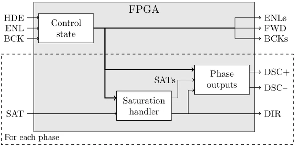
7 Implementation 34 7.1 Internal function blocks . . . 347.1.1 Control state . . . 34
7.1.2 Saturation handler . . . 35
7.1.3 Phase outputs . . . 36
7.1.4 Supervision outputs . . . 36
7.2 Additional functionality - deadband control . . . 36
7.2.1 State transition timer . . . 37
7.2.2 Saturation timer . . . 37 7.2.3 Phase outputs . . . 38 7.3 Timing . . . 38 7.3.1 Clock source . . . 38 7.4 State encoding . . . 39 7.4.1 Forming outputs . . . 40 7.5 Gate driver . . . 40 7.5.1 Minimum change . . . 41
7.5.2 Dedicated driver chip . . . 41
7.5.3 Modified discrete driver . . . 41
8 Simulation 44 8.1 VHDL . . . 44 8.2 Gate driver . . . 44 9 Prototype 45 9.1 Breakout board . . . 45 9.2 Custom PCB . . . 45 10 Test setup 47 10.1 Logic functionality . . . 47 10.2 Interfacing a drive . . . 47
10.2.1 Control board modifications . . . 47
10.2.3 Measurement accuracy . . . 48 10.2.4 Saturation detection . . . 49 10.2.5 Power consumption . . . 49 10.2.6 Deadband timing . . . 50 11 Test results 51 11.1 Response times . . . 51 11.2 Measurement accuracy . . . 56 11.3 Power consumption . . . 57 11.4 Deadband timing . . . 61
III
Evaluation
65
12 Evaluation 65 12.1 Performance . . . 65 12.1.1 Logic . . . 65 12.1.2 Gate drive . . . 65 12.2 Cost . . . 65 12.3 Area . . . 66 12.4 Safety considerations . . . 6712.4.1 Metastability and race conditions . . . 67
12.4.2 Clock oscillation . . . 68 12.4.3 Redundancy . . . 69 13 Summary 70 13.1 Conclusions . . . 70 13.2 Future work . . . 71 13.2.1 Clock source . . . 71 13.2.2 Added functionality . . . 71 13.2.3 Programming . . . 71 13.2.4 Reliability . . . 71
Acronyms
ADC analogue-to-digital converter. 13, 24, 48, 49, 57 AEC Automotive Electronics Council. 28
ASIC application specific integrated circuit. 24 BGA ball grid array. 28, 45, 67
CAD computer aided design. 61, 71 CAN controller area network. 48
CMOS complementary metal oxide semiconductor. 31, 47 CPLD complex programmable logic device. 24–26, 36, 45 CPU central processing unit. 24
DAC digital-to-analogue converter. 24
EEPROM electrically erasable programmable read-only memory. 25 EMC electromagnetic compatibility. 28, 71
EMI electromagnetic interference. 26 ESD electrostatic discharge. 28 FIT failure in time. 71
FPGA field programmable gate array. 1, 24–26, 31, 36, 40, 44, 45, 47–49, 51–56, 61–69, 71
FSM finite state machine. 13, 25, 34–36 HDL hardware description language. 2, 29, 34 I/O input/output. 20, 21, 27, 36, 41
IBIS input/output buffer information specification. 45
IC integrated circuit. 20, 21, 27, 31, 32, 41, 42, 45, 48, 49, 65, 67, 69, 71 ISR interrupt service routine. 24
JTAG Joint Test Action Group. 29, 45 LDO low dropout regulator. 20, 49 LE logic element. 24, 25, 44, 45, 67 LSB least significant bit. 57
LUT lookup table. 24–26
LVCMOS low voltage CMOS. 20
LVTTL low voltage transistor-transistor logic. 20, 21, 41 MC macrocell. 24–26, 36
MCU microcontroller unit. 13, 14, 17, 20–22, 24, 27, 30, 31, 36–38, 41, 44, 47, 48, 53, 54, 68, 69
MEMS microelectromechanical system. 31
MOSFET metal oxide semiconductor field effect transistor. 6, 7, 10–12, 14, 17–21, 23, 27, 35–38, 40–42, 44, 47, 61, 65, 68, 70
MSM maximized saturation method. 1, 2, 6, 47 PAL programmable array logic. 36
PCB printed circuit board. 2, 3, 29, 31, 32, 45, 66, 67, 71 PCBA printed circuit board assembly. 36, 65
PIA programmable interconnect array. 25
PLD programmable logic device. 1, 2, 20, 21, 24, 25, 27–30, 32, 34, 36, 38, 40–42, 44, 67, 69–71
PLL phase-locked loop. 26, 31, 45, 68
PMSM permanent magnet synchronous machine. 1 PWM pulse-width modulation. 41
RoHS directive on the restriction of the use of certain hazardous substances in electrical and electronic equipment. 27
SDC Synopsys design constraints. 29 SMD surface mounted device. 46
SRAM static random access memory. 24, 25 TQFP thin quad flat package. 45, 67
VFD variable frequency drive. 1, 5, 13, 21, 47
VHDL very high speed integrated circuit hardware description language. 29, 34, 38, 51, 68
1
Introduction
Inmotion Technoligies AB develops and manufactures equipment for the indus-trial vehicle industry. A major part of this are the variable frequency drives (VFDs) that control the permanent magnet synchronous machines (PMSMs) or induction motors used for propulsion of vehicles.
The current in each phase of the motor needs to be known to control the motor. Therefore, an integral part of the drive is the current measurement. These measurements require consideration when scaling up to applications using high voltages and currents.
One field which has seen a significant increase in recent years is the area of heavy hybrid vehicles. These motors and drives operate at higher voltages and currents than their light weight vehicle counterparts. To accommodate this, Inmotion use a special measurement technique in their high voltage drives called the maximized saturation method (MSM).
This technique achieves high precision and efficiency at high powers while avoiding the cost and weight increases other approaches would bring. The draw-back is the requirement for more complex control logic.
1.1
Previous work
One of the first to propose this method of current measurements was the Swiss company Socapel SA [1], later acquired by what is now Inmotion. This was tested for higher currents by Inmotion under the company name of Atlas Copco Controls [2].
Two master’s theses have been written on the subject of this method. The first one focused on the electromagnetic properties of the measurement trans-former coils [3]. The other worked on the development of the discrete logic controller [4]. Both were performed at Inmotion although the company name at the time was Danaher Motion and Kollmorgen respectively.
1.2
This report
With increased safety requirements and a demand for drives controlling more than one three-phase motor, the size of the control logic in these drives has grown to a considerable size. A more modern and compact solution is therefore desired. This report investigates an approach towards this by moving the current measurement control logic from an implementation consisting of many discrete components into a single programmable logic device (PLD).
While programmable logic has been around for a while, most applications can be divided into two groups. One is the replacement of a few very simple logic functions with one low density PLD. The other, which has seen a big increase in usage over the past decade or so, is the utilisation of high density PLD for reconfigurable hardware acceleration in data intensive computing and communication applications.
The application in this report does not quite fit into either of these two groups. The functionality is more complex than a few small combinatorial logic nets or a shift register but not nearly on the level where developers often look into field programmable gate arrays (FPGAs).
Other factors making the application atypical is the close connection to the physical world and the need for safe and reliable operation while at the same time being cost effective. With the intention of using this in series production instead of jellybean parts renders it is much more cost sensitive than for instance a hardware simulation test bed.
While this method for measuring current is known from before and have been used by Inmotion in a few products, it is still fairly uncommon and far from an industry standard. Despite being described in previous theses and other reports, it has seen several changes over the years and may have more to come. For this reason, the flexibility in a programmable hardware has the potential to be very advantageous. It also makes it an interesting application from a technical standpoint.
The work going into this report started with an analysis of the measurement method in its present implementation as well as the workings of PLDs in order to break down the intended application into requirements for selecting a device. Limitations arising from the new type of implementation were also identified. The PLD market was investigated and a suitable device chosen.
The control for the maximized saturation method based on the existing input signals was then developed in several steps. The functionality was broken down into necessary code blocks which were written, simulated and tested in evaluation hardware.
Possibilities for extended functionality made possible by the intended new implementation were also investigated and an alternate setup was developed. A custom printed circuit board (PCB) was designed to support both the simple and the extended version.
Test were performed on a product in production to set a baseline. The custom hardware was assembled and necessary modifications to the existing hardware were performed to interface the custom board. The custom board was tested as part of the existing product and performance was compared.
The economic effects of such a change for a production part were estimated and things to consider both in a more general sense and for this application in particular were summarised. Altogether this report tries to investigate the possible impact of moving to programmable logic from a wide perspective in applications where it might not be the first choice to come to mind.
1.2.1 Structure
This report is divided into three major parts. Part one explains the theoreti-cal background. Theory for current measurements and the motivation for this method is given in Section 2. Section 3 gives a background into why an extended functionality in the logic with a controllable deadband could be an improvement when controlling the magnetic flux in an inductor with an H-bridge. Section 4 analyses how the circuits in the existing implementation work. Section 5 gives a brief summary of different types of programmable logic devices and the re-quirements for choosing one for this particular application. Section 6 discusses options for generating a necessary clock signal.
Part two is about implementing this functionality with a PLD. Section 7 de-scribes how the hardware description language (HDL) code setup is structured. Simulation and development of the prototype board is described in Sections 8
and 9 respectively. Section 10 explains the test setup used for evaluating it and the results are given i Section 11.
Part three evaluates the results from the practical tests as well as other fac-tors affecting the choice of implementation such as economics and PCB area. In Section 13 conclusions are drawn, things to consider when moving to pro-grammable logic discussed and a few topics to look further into are mentioned.
Part I
Theoretical background
2
Current measurement
A common and simple way of measuring currents is by using a shunt resistor. The current is passed through a low valued resistor and the voltage over the resistor is measured directly. The current can then be calculated through Ohm’s law, I = U/R.
One big disadvantage of this method is that the voltage sensing electronics need to be directly connected to the conductor through which the current is flowing, in this case the energized motor cables. Even though the measured voltage differential over the resistance is low, the common mode voltage swing can be very high, putting high requirements on the electronics. The electrical connection is also undesirable from a safety standpoint as a component failure may provide a current path to other parts of the circuit or vehicle. To solve this problem, some sort of galvanic isolation is required.
2.1
Measurement transformer
A common way of achieving galvanic isolation is by using a measurement trans-former, feeding the current to be measured through the primary winding and connecting the shunt resistor to the secondary. This also enables the current to be scaled up or down according to the turns ratio of the transformer coils.
In the case of an ideal transformer, where there are no leakage inductances or core losses and the permeability is infinite, the relationship between the magnetic field strength H, current i and number of turns N as given by Amperes law can be written as (2.1) if the field is also homogeneous.
I
H· dl = Z
A
J· dA = N i (2.1)
The magnetic field is the same for the primary and secondary windings as they are wound on the same core. According to Faraday’s law (2.2) the voltage u(t) over a coil is equal to the time derivative of the linked flux ψ, or the flux φ through each individual turn times the number of turns N , so the relationship between current and voltage in the coils is constant, giving (2.3).
u(t) = dψ dt = N dφ dt (2.2) u1 N1 = dφ dt = u2 N2 (2.3) The magnetic energy W stored in an inductor is given by (2.4). L is the inductance as given in (2.5) where l is the magnetic length, A is the cross sectional area of the core and µ is the permeability as in (2.6) [5][6]. If the cross sectional area of the coil is small relative to its diameter, the assumption that the magnetic field is homogeneous over the cross section is a good approximation [7]. Combining these results with (2.1) gives the relationship (2.7).
W = 1 2Li 2 (2.4) L = N 2 l µA (2.5) B= µH = µrµ0H (2.6) W = 1 2µH 2 Al (2.7)
Consequently the stored magnetic energy depends on the volume of the core, its permeability and the H-field which in turn depends on the current and number of turns in the coil. Note that µr is not a constant but has a non-linear
relationship with B for other materials than vacuum.
B
H
Figure 2.1: Hysteresis curve for a ferromagnetic material.
For ferromagnetic materials the value of µris very high, on the order of 50000
for the core used here, and very little current is needed to create a big change in the magnetic flux density B. As the B-field approaches a high enough level, the value of µr tapers off towards one as depicted in Figure 2.1. When this point
has been reached, an increase in primary current will not change the magnetic flux noticeably and thus will not be seen at the secondary. Measurement values calculated with the nominal value of µr in the linear region will therefore no
longer be valid.
Since a VFD naturally must be able to operate at very low frequencies and thus long periods while handling large currents, a normal measurement transformer would have to be very large in order not to saturate. This becomes impractical and expensive.
Another important effect of saturation is that since the value of µ in (2.5) approaches one, the inductance is significantly lowered.
2.2
Hall-effect method
Another method is to use a transformer which has an air gap with a hall effect sensor in it. The Hall-effect sensor measures the B-field in the core as a voltage directly, using the Hall effect.
As current passes through a magnetic field, the Lorentz force will act on the electrons forcing them to one side of the conductor. This generates a voltage perpendicular to both the current and the magnetic field which can be measured directly.
Either this reading is used directly, or it is used in a control loop applying a current to a secondary control winding. The current in the control winding is adjusted to cancel the magnetic field induced by the primary. The required current for cancellation is then measured using a shunt resistor. This current and voltage source can operate at a lower level than the measured currents according to the turns ratio of the transformer and it also benefits from the galvanic isolation.
The air gap reduces the risk of saturating the core and in the closed loop configuration the risk of saturation is avoided even further giving the opportu-nity to use a smaller transformer core. However, power is required continuously to regulate the field in the core.
The main disadvantage of these methods is the limited accuracy coupled with the relatively high cost of the Hall-effect sensors. In high power applications such as in the drives for high voltage motors in hybrid vehicles it is necessary to be able to measure high currents with good precision. For this reason, at Inmotion, the use of Hall-effect sensor based current measurement is limited to low power drives.
2.3
Maximized saturation method
At Inmotion Technologies, another measurement technique has been used in a couple of motor drives. This method borrows some of the elements of the Hall methods. It utilises the idea of applying a voltage to the secondary coil but instead of controlling the flux to a minimum at all times, the core is only driven out of saturation right before sampling. This reduces the mean power required to control the flux density compared to the closed loop Hall-effect method and does not require an air gap.
The core is allowed to saturate in between measurements, hence the name. This lowers the inductance seen at the primary coil and also reduces the current generated in the secondary as the derivative of the flux is lowered in (2.2). The energy dissipated as heat in the shunt resistors is therefore lowered in between measurements.
The material used for the magnetic cores in this system was originally a proprietary cobalt alloy with a very steep hysteresis curve and a sharp transition into saturation at around 0.58 T [8] which makes it suitable for this application. Later on this has been changed to cores from another manufacturer with similar magnetic properties.
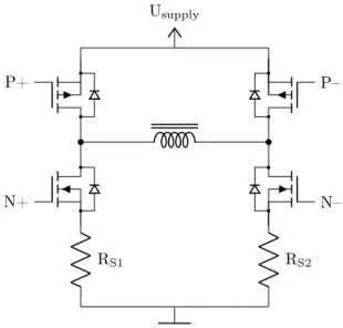
2.3.1 H-bridge
To drive the current in the secondary winding, an H-bridge is used. This consists of four metal oxide semiconductor field effect transistors (MOSFETs) in the
Usupply RS1 RS2 P+ N+ P– N–
Figure 2.2: H-bridge controlling the secondary current.
configuration shown in Figure 2.2. This allows current from the power supply to be passed in either direction of the coil as well as let the coil be either open or short circuited through the shunt resistors to ground. The H-bridge is driven into four different states as follows, depicted in Figures 2.3 through 2.5. Forward One of the diagonal pairs of MOSFETs, either P+ and N– or P– and N+ turns on, driving current from the supply voltage through the secondary coil. Which of the pairs is determined by the flux in the core. The current direction is applied to counteract the field induced by the primary coil, i.e., the motor current.
Back This is the reverse of the Forward state. The other diagonal pair is turned on, inducing a field in the core with the same direction as the one induced by the primary.
Measure In this state, N+ and N– are conducting. This is effectively short-circuiting the coil through the two shunt resistors.
Idle The idle state turns off all the MOSFETs. The secondary coil is open-circuited except for the body diodes of the MOSFETs. These will however only conduct current if the voltage over coil is greater than the supply voltage plus the forward voltages of the two body diodes.
2.3.2 Saturation detection
As the saturation results in a significant reduction of the coil inductance, the current in the coil will increase rapidly. It is important to detect this in order to switch off the power and limit the current rush. This is done with a comparator,
Forward. On Off Off On i i Back. Off On On Off i i Measure. Off On Off On i Idle. Off Off Off Off
Figure 2.3: Nominal secondary current direction in the different states.
comparing the voltage over the shunt resistors to a reference. When too big a current is detected, the core is assumed to be saturated and the H-bridge switches into the measurement state. If this is not done quickly enough, the power consumption will increase significantly and excessive stress is put on the components.
2.3.3 Current direction
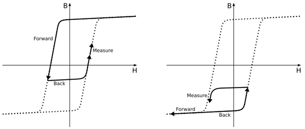
The earlier methods [1] and [2] always saturate the core in one direction during the forward pulse independent of the actual current direction in the motor phase. Then the Back-pulse drives it back into the linear region. This is not the most efficient use of power since one measurement may require up to a full loop of the hysteresis curve.
This is improved upon by taking the direction of the last measurement into account in the implementations [3] and [4]. This way the forward-pulse direction should never have to drive the core from one saturated state to the other and power is saved, at the expense of added circuit complexity.
This is done in slightly different ways. The implementation described by Lindgren [3] assumes the core to be saturated at the start of every measurement cycle. A forward pulse is applied to drive the core out of saturation. The measurement state is entered and a sample is taken. Then a back pulse is applied to drive the core back into saturation. This approach causes some samples to
B
H
Forward
Back
Measure
Figure 2.4: Normal operation.
B
H
Forward
Back Measure
Figure 2.5: Saturation detected. be invalid as the assumption of a saturated core before the desaturation is not valid when the primary current has changed sign since the last measurement.
The more recent implementation described by Wisten [4] on the other hand always applies both the forward and the back pulse before doing the measure-ment. This back pulse is shorter than the forward pulse in order not to drive the core back into saturation, see Figure 2.4, but long enough to drive the core back into the linear region in the case of the forward pulse being interrupted by saturation detection, see Figure 2.5. If that happens, this implies that the sign of the primary current has changed and a flip-flop that stores the information on current direction is toggled. The following measurement cycle will have the opposite direction for the states forward and back.
2.3.4 Idle state
Another difference between the two implementations [3] and [4] is the choice of state in between measurements. While [3] uses the measurement state to reduce the drift of the magnetic flux, [4] opens all the MOSFETs to instead let the flux drift easily and reduce power loss in the shunt resistors in between measurements. The latter method is the one currently used in both regards.
3
Deadband
When using MOSFETs as switches, the current is not immediately turned on or off with the control signal. There is a slight delay and the channel current iDS changes with the charge or discharge of the gate capacitance.
When using them in a half bridge configuration there is a need to delay the turn-on of one a while after the turn-off of the other. This is called deadband as there is a time during the transition from the high to low MOSFET conducting or vice versa when none of them are turned on. Without this feature the half bridge would experience what is called shoot-through, i.e., both MOSFETs are conducting simultaneously, shorting the supply to ground.
The transition times are longer for P-channel than N-channel MOSFET since electrons have higher mobility than holes [9]. They also generally have a higher input capacitance making the transition slower as well as higher channel resistance, RDS. For this reason many applications use an N-channel MOSFET
for the high side as well as the low side. This does however require a gate voltage higher than the supply for the high side to turn it on efficiently. This can be solved with a bootstrap capacitor which is charged up when the low side is conducting and then supplies the high side gate driver when the low side is turned off.
This type of solution has the limitation that the low side has to be turned on occasionally to charge the capacitor. A duty cycle of 100% is therefore not possible. For this application this is not a problem since the measure state is entered every cycle with both low sides turned on but it is using a rather low switching frequency with a long delay between the measure state and the next forward, requiring the bootstrap capacitor to hold its charge for a long time.
Bootstrapping also requires a bit more complicated circuitry and, since the MOSFETs used here have a low RDS of around 20 mΩ even for the P-channels,
it is not used here.
3.1
Miller effect
Usupply
Coil P
N
Another consideration when swithing the MOSFETs is the Miller effect. All transistors have parasitic capacitances between the leads. These are generally very small, on the order of a few pF. The capacitance from gate to drain in an inverting amplifier is however multiplied by the amplification plus one and thus appears to be significantly larger [9].
When switching one MOSFET of a half bridge, the voltage change at the drain is coupled through this capacitance to the gate of the other MOSFET and adds to its gate voltage. If the turn-on of one MOSFET occurs before the gate voltage of the other has discharged to a low enough level, this voltage spike can turn on the MOSFET and cause shoot-through.
To mitigate both of these problems, the turn-on of one MOSFET in a half bride is delayed some time after the turn-off of the other. This lets the first gate capacitance discharge to a safe voltage level and is called a deadband since there is a time in each switching occurrence where none of the MOSFETs are turned on.
4
System analysis
The VFD consists of several modules for different tasks such as power supply, communication, supervision, current measurement, etc. All these modules are governed by a main microcontroller unit (MCU) as well as a supervision MCU. This thesis concerns the current measurement unit. It receives two signals from the main MCU: Enable (ENL) and Back (BCK). Based on these pulses, the current measurement module should return valid voltages representative of the motor currents to the analogue-to-digital converters (ADCs) at the correct time. The voltages are sampled at a frequency of 4 kHz, i.e., the pulses start with an interval of 250 µs. The ENL-pulse has a duration of around 20 µs. The BCK-pulse starts 10 µs into the ENL and lasts for 5 µs. The exact values may be reconfigured but the resulting duty cycle for ENL lies around 8 %.
4.1
Discrete implementation
The logic in place today for controlling the H-bridge from these pulses is made up of a mix of analogue and digital circuits with an emphasis on the latter. Together they implement the finite state machine (FSM) depicted in Figure 4.1 for each phase. These circuits can be divided into a couple of blocks as follows, with prevalent signals summarized in Table 4.1.
off start idle frwd back meas meas meas HDE=1 ENL=1 SATF=0 BCK=1 BCK=1 BCK=0 SATB=0 BCK=0 ENL=0
Figure 4.1: State diagram.
Signal Full name Origin
ENL Enable Main MCU
BCK Back Main MCU
SAT Saturation Comparators
FWD Forward Figure 4.2
DSC Driver state control Figure 4.4 SDL Saturation detection latch Figure 4.4
DIR Direction Figure 4.5
HDE High-side driver enable Figure 4.7 Table 4.1: Summary of signals.
4.1.1 Forward pulse generation R S BCK Q ENL ENL FWD
Figure 4.2: Logic to produce the Forward-pulse.
The two pulses from the MCU are fed to the network of NOR-gates shown in Figure 4.2. The leftmost is wired up as an inverter giving the output of ENL. The centre two that feed back into each other form an active-high SR-latch with BCK connected to Set and ENL to Reset. The output of this latch, Q, is combined with ENL in the rightmost NOR-gate to form the forward-pulse.
-5 0 5 10 15 20 t[µs] ENL BCK = S ENL = R Q FWD
Figure 4.3: Signals involved in the Forward-generation.
The signal sequence is shown in Figure 4.3. At the start of every measure-ment cycle, Q is low. When ENL goes high, its inverse ENL goes low. The latch retains its low value and FWD goes high. At the rising edge of BCK, the latch is set and FWD goes low. When BCK falls back down, Q remains high until the falling edge of ENL where Q is reset. FWD is kept low until the next enable-pulse.
4.1.2 Combinational logic
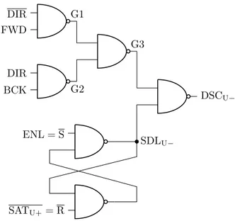
The currently available signals: ENL, FWD and BCK along with the saturation signals as well as the signal DIR and its inverse, which keep track of the cur-rent direction in the phase, are combined in the circuit depicted in Figure 4.4. The output signal DSCU− is fed to the MOSFET-driver circuitry described in
DSCU− G1 G2 G3 DIR FWD DIR BCK ENL = S SATU+= R SDLU−
Figure 4.4: Signals to drivers.
The input connections in Figure 4.4 are for the negative terminal of the coil of phase U in motor 1. For the positive counterpart DSCU+, the DIR and DIR
signals are interchanged and the SAT+ signal is changed to SAT− coming from the other comparator. The other phases have equivalent combinational circuits. The lower part is once again an SR-latch but this time active-low. At the end of a measurement cycle, when ENL goes low, the latch is set giving SDL a high level. If the comparator output SAT+ goes low due to core saturation, SDL is reset to a low value for the rest of the enable pulse. The value of DSCU−
is given by equation (4.1) and presented in Table 4.2. DSCU− = SDL · G3 G3 = G1 · G2 G1 = DIR · FWD G2 = DIR · BCK =⇒
=⇒ DSCU− = SDL · DIR · FWD · DIR · BCK = = SDL + (DIR + FWD) · (DIR + BCK) = = SDL + DIR · DIR | {z } =0 +DIR · BCK + FWD · DIR + FWD · BCK (4.1)
From (4.1) follows that whenever SDL is low, DSC is high. The results for the other signals are shown in Table 4.2. FWD and BCK are mutually exclusive so the only valid combinations giving a low value on DSCU− are FWD · DIR
and BCK · DIR. For the positive side half-bride, the signs of DIR and DIR are interchanged.
SDL DIR FWD BCK DSCU− 0 X X X 1 1 0 0 0 1 1 0 0 1 1 1 0 1 0 0 (1 0 1 1 0) 1 1 0 0 1 1 1 0 1 0 1 1 1 0 1 (1 1 1 1 0)
Table 4.2: Truth table for DSCU−. 4.1.3 Direction control
The outputs of the comparators for saturation detection are normally pulled high by pull-up resistors. When they are triggered by the shunt resistor voltage exceeding the reference voltage, their output is pulled low resetting the latch marked SDL in Figure 4.4.
The latched comparator signals SDL of both sides of the coil are connected to an AND-gate. The output of this gate is connected to the clock input of a D-type flip-flop as shown in Figure 4.5. The output from the flip-flop is the signal DIR and the complementary is DIR. The complementary output is also fed into the flip-flops data input.
D Q CLK Q SDL+ SDL− DIR DIR
Figure 4.5: Direction memory.
If either of the comparators detects saturation, their respective latch will be reset. The AND-gate connected to the clock input will go low and stay low until the latch is once again set by the falling edge of the Enable-pulse. This rising edge will toggle the state of the flip-flop and the values of DIR and DIR.
The use of two different comparators and latches makes it possible to inhibit the low signal of DSC on one side due to saturation while the other still oper-ates normally. If saturation is detected during the forward pulse, for instance when DSCU− is low, this signal will go high at saturation. During the following
BCK pulse, DSCU+ can still go low unless it is also interrupted by saturation.
Normally saturation will only occur during the Forward pulse but having pro-tection against it during the Back pulse is still preferable and which half bridge is active during forward depends on DIR.
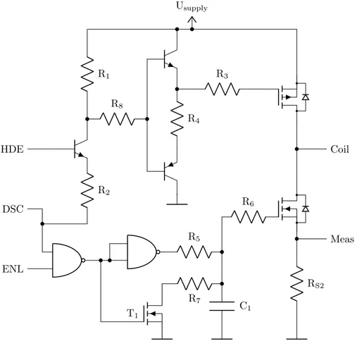
4.1.4 Gate drivers
Driving the H-bridge is a bit more complicated than assigning logic levels to the gates of the MOSFETs. The drain-to-source resistance and switching speed of the MOSFETs depend on the applied gate-to-source voltage. Higher voltages result in quicker switching. At the same time the MOSFETs cannot withstand the full 27 V of the supply from gate to source but is limited to ± 16 V for the N-channel and ± 20 V for the P-channel. These voltages are also referenced differently with the source connected to ground and supply respectively.
To accomodate this, the circuit depicted in Figure 4.6 changes the voltage to appropriate levels and also provides some logic functionality.
DSC ENL HDE Usupply T1 Coil Meas R1 R8 R4 R3 R2 R5 R7 C1 R6 RS2
Figure 4.6: MOSFETs and driver for one coil terminal of one phase. This block takes the inputs ENL from the MCU and DSC from the circuit in Figure 4.4 and controls the power MOSFETs in order to connect one terminal of the secondary coil to either the supply (+, 27V), through the shunt resistors to ground (–) or none (Z) according to Table 4.3.
It is worth noting that DSC only goes low during the forward or back pulse which in turn only occurs during an ongoing enable. The state where both DSC and ENL are low will therefore never occur. The possible signal combinations
ENL DSC Coil
(0 0 +)
0 1 Z
1 0 +
1 1 –
Table 4.3: Coil state according to signals.
and the corresponding states of the MOSFETs are displayed in Table 4.4.
State ENL DSC+ DSC− P+ N+ P– N–
Idle 0 1 1 off off off off
Forward 1 0 1 on off off on
Back 1 1 0 off on on off
Measure 1 1 1 off on off on
Table 4.4: MOSFET control signals.
This circuitry includes a deadband feature, making sure that there is a delay between turning off the P-channel and turning on the N-channel.
When ENL and DSC are high, the low side gate is charged from the NAND-gate through R5 and R6. The MOSFET connected to R7 is turned off. The
capacitor to ground increases the turn-on time of the low side power-MOSFET. When DSC goes low, the MOSFET opens, allowing a quick discharge of the gate and capacitor on the low side. Current flows through both R7 via the
MOSFET and through R5 via the NAND-gate to ground.
4.1.5 Boot-up protection
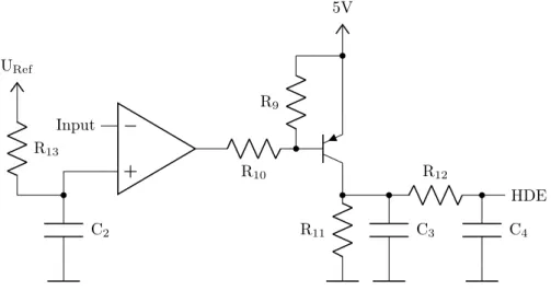
An NPN-transistor, apart from a transistor, also forms a diode which can con-duct current from the base to the collector. This is generally not a problem as the collector potential is normally higher than the base. During system start-up however there is a possibility that the 27 V sstart-upply rises slower than the 5 V. Current can then pass through both the NPN-transistors in the circuit up to the 27 V supply while the gate of the P-channel MOSFET is still low. The voltage over the P-channel MOSFET can cause it to turn on and result in shoot-through.
To mitigate this problem there is a resistor R8 in this path. More
impor-tantly, the input HDE is kept low initially to avoid spurious signals turning on the P-channels at start-up. When the system has booted, this input is kept at 5 V unless the supply voltage falls below a certain threshold.
Figure 4.7 displays the circuit controlling this. It compares an input signal of 0−3.3 V to a reference voltage. The comparator has an open collector output which is pulled up to 5V by R9. The output of the circuit is pulled to ground
by R11. The PNP-transistor reduces the output impedance and is turned on
when the comparator output goes low.
Apart from stepping up the signal voltage from 3.3 to 5 V this circuit in-creases stability of the signals during boot-up. The comparator output is more deterministic than logic gates before the supply reaches its nominal value.
− + URef R13 C2 Input R10 5V R9 R11 R12 C4 C3 HDE
Figure 4.7: High-side driver enable circuit.
4.2
Delays
One of the most critical timing factors in the application is the time it takes from the core going into saturation until the forward-pulse is turned off. If full power is continuously applied after saturation, the MOSFETs will be destroyed in a couple of microseconds.
Comparators When the voltage over the shunt resistor exceeds the reference, the comparator output goes from high to low in about 300 ns.
Combinational logic From the comparator to the signal DSC, there are three gates with a worst case propagation delay of 9, 9 and 17 ns respectively resulting in 35 ns in total.
When changing state, for instance going from forward to back, the path is a bit longer with a worst case delay of 59.5 ns.
Driver circuit The driver circuit has by design different state transition times for different directions. When DSC goes from high to low, the low side starts to turn off after around 40 ns and after around 80 ns the coil terminal has levelled out at a voltage in between ground and supply. The coil terminal is basically floating at this point. 105 ns after the falling edge of DSC, the P-channel starts conducting and the coil is connected to the supply after around 220 ns. Figure 4.8 depicts these transitions together with the voltages at the gates. For increased visibility the coil voltage has been divided by five and the P-gate voltage has been shifted down by 22 V.
When the signal DSC goes from low to high, the coil starts to drop from the supply voltage after 40 ns levels out midway after 70 ns. After 160 ns it starts to drop towards ground and reaches a low level after around 250 ns which can be seen in Figure 4.9.
At saturation, the forward state transitions into measure so the latter case applies. In the simulation, the propagation delay of the logic gates in the driver
circuit was omitted so only the rise times were included. This could delay the turn-off of the N-channel by up to 9 ns and the turn-on by 20 ns more.
The actual curves would be largely affected by the big inductive load and the transformed current during operation. Simulation was done with a mainly resistive load since the sought after result was the behaviour of the driver it-self. Furthermore, simulation was severely slowed down by the induced current through the body diodes generating singular values in the model of the power-MOSFETs when including a large inductance.
4.3
Available power
The power board supplies a lot of different voltages around the system. The current measurement board uses a couple of them in the current implementation. The H-bridge and its drivers are fed by 27 V. The comparators use a 15 V source. Most of the discrete logic use a 5 V source while the NOR-gates generating the forward -pulse use 3.3 V power.
The 3.3 V supply is generated by a low dropout regulator (LDO) capable of delivering 800 mA of current. This supply is in turn fed 5 V from another LDO capable of delivering 1 A.
4.4
Interfacing
As the main objective of this project is to investigate a change from the discrete logic into programmable logic it is reasonable to try and leave as much of the other circuitry unchanged as a first approach. If only the circuitry taking the pulses from the MCU and the comparators to produce the signal DSC were to be changed, this would result in replacing the integrated circuit (IC) packages in Table 4.5. This amount of circuits could possibly on its own motivate a migration into programmable logic. This section explains the interfacing of this circuitry towards the rest of the system.
Function Single drive Dual drive
4×2-NAND 9 18
4×2-NOR 1 2
2-AND 3 6
D-flip-flop 3 6
Total 16 32
Table 4.5: Replaceable logic chips when maintaining drivers and comparators.
4.4.1 Inputs
The MCU runs from the the 3.3 V supply. The two input pulses ENL and BCK it sends to the current measurement circuit are therefore at that level. The logic gates they are fed into work from a 5 V supply but they accept 3.3 V low voltage transistor-transistor logic (LVTTL) or low voltage CMOS (LVCMOS) levels as input.
The comparators for saturation detection have an open collector output pulled up to 5 V by a resistor each. Most modern PLDs support 3.3 V in-put/output (I/O) logic levels but some are tolerant to 5 V inputs. If this is not
the case then the pull-up configuration can still be adapted to use 3.3 V instead rather easily.
The comparators used support tying the outputs together for logic AND functionality. This implies that the input signals to the circuit could be reduced to one rather than two saturation signals per phase, plus the two signals from the MCU.
4.4.2 Outputs
The MOSFET-drivers still include one NAND-package per phase, two gates per half-bridge in the low-side driver. While there is a MOSFET sinking the gate of the N-channel to turn it off, the logic IC in place provides the 5V to turn it on. The 3.3 V output of most PLDs is not enough to achieve good and robust performance in driving the N-channel MOSFET gates high. The NAND-gates would serve the added purpose of logic level shifters.
Removing these NAND-gates would also require supplying the complemen-tary signal of DSC from the PLD to control the signal-MOSFET if the driver circuitry is otherwise left unaltered. In the current configuration, the combina-tional logic supplies the signal DSC while ENL can be routed directly from the MCU.
The high-side driver, i.e., the circuitry controlling the P-channel power-MOSFET, is also interfaced using the signal DSC. When this goes low, the NPN-transistor turns on. The gate outputting DSC must therefore be able to sink the current from the emitter, which in the current configuration is around 11 mA.
For this reason, another type of NAND-gate is used here than for most other places where a 2-input NAND gate is required. This type is slower and does not accept LVTTL input levels but it has a higher drive strength. Although the rated absolute maximum output current is the same for both types, the equivalent output impedance of this type is lower and thus can maintain the low voltage at the transistor emitter more easily.
For many PLDs this would be a limiting factor. However, if the PLD has more I/O ports than the minimum requirement, several outputs could be used together in order to increase the drive strength.
Another consideration in interfacing the high-side driver is that the base of the NPN-transistor is now tied to 5 V (HDE). When DSC reaches this value, it turns the transistor off. This voltage may not exceed the maximum output level of the PLD. If necessary, this can be changed by modifying the supply and R9 of the circuit in Figure 4.7.
Another solution to both of these problems would be to replace the whole circuitry with a gate driver IC. An added benefit is the more explicit control of the deadband. This would however require four signals to the driver circuitry per phase instead of the present two per phase plus the global ENL, which is common to all the phases.
4.5
Supervision
The VFD contains a supervision MCU which aids the main MCU in performing a couple of periodic controls to ensure that the system operates as intended.
4.5.1 Control state timing
One such check is that the pulse lengths of ENL, BCK and FWD are monitored. This is to verify that the samples are taken at the correct time and thus at the correct point of the hysteresis curve and not in or close to saturation.
4.5.2 Direction update
Periodically the MCU puts out a FWD pulse of excessive length to deliberately loop through the whole hysteresis curve and trigger the saturation detection. This is done to verify that the direction signal, DIR, toggles. As mentioned this consumes some extra power, hence it is not done for every sample.
4.5.3 Sum current
The sum of the currents in each phase of one motor should add up to zero. This property has earlier been used to determine the current of the third phase while only actually measuring two.
To increase redundancy and detect errors, the third phase measurement is now also performed. If the calculated and measured values do not match, this implies that something is faulty and the system shall invoke a safe state.
0 100 200 300 400 500 0 1 2 3 4 5 Time [ns] V o lt a g e [V ]
Simulated voltages with resistive load
DSC P-gate –22
N-gate Output/5
Figure 4.8: Falling edge of DSC, signaling the gate driver circuitry to turn off the low side and turn on the high side MOSFET.
0 100 200 300 400 500 0 1 2 3 4 5 Time [ns] V o lt a g e [V ]
Simulated voltages with resistive load
DSC P-gate –22
N-gate Output/5
Figure 4.9: Rising edge of DSC, turning off the high side and turning on the low side.
5
Programmable logic devices
A popular choice when trying to increase flexibility and minimizing parts count in electronic systems it to integrate functionality into a central processing unit (CPU) or an MCU. These are generic and multi purpose and are easy to write software to in order to create the desired functionality. Because of their widespread use, some have been more adapted towards certain ranges of use and incorporate hardware such as comparators or ADCs and digital-to-analogue converters (DACs).
The big drawback is that all actions are performed sequentially. While the state machine described here could be implemented in an MCU, it would take several clock cycles to change state or output according to the current input. The reaction times can be improved by using interrupt branching but still only one interrupt service routine (ISR) can be executed at any one point in time, one line of code at a time. For logic hardware the reaction times can theoretically be reduced to one clock cycle since all the inputs, outputs and intermediate logic work in parallel [10].
PLDs are another type of customizable chips where the written code defines the physical layout of the hardware rather than the actions taken in the software of a processor.
5.1
Architectures
PLDs come in a range of different sizes, from small ones replacing a few logic gates to chips that contain millions. The smallest ones are too simple to be useful in this project but the medium to high capacity PLDs can be divided into the categories below.
5.1.1 Field Programmable Gate Array (FPGA)
This type of PLD was first intended for prototyping of application specific in-tegrated circuits (ASICs) at lower clock speeds during development. Nowadays it is a common choice for high density PLDs and offers high flexibility without the big overhead cost of producing an ASIC.
The main building block or logic element (LE) generally consists of a couple of 3- or 4-input lookup tables (LUTs) and a D-type flip-flop. A 4-input LUT is basically a multiplexer with 16 inputs, all pre-programmed to a value. The output can thus implement an arbitrary logic function of the four address inputs. These LEs are interconnected in a big configurable matrix.
FPGAs are common for large scale, data intensive logic functions such as signal processing or as a customizable CPU core.
The configuration is generally stored in a static random access memory (SRAM). This is a volatile memory type and needs to be loaded at startup from an external non-volatile memory which adds a bit of extra circuitry [11]. 5.1.2 Complex Programmable Logic Device (CPLD)
For small to medium sized applications the use of a CPLD instead is rather com-mon. These consist of a number of macrocells (MCs) which are interconnected similarly to the LEs of the FPGA.
The MC in itself has the structure of a small PLD which forms a sum-of-products logic output through a programmable interconnect array (PIA) of gates. A CPLD has a lower number of MCs than an equivalent FPGA has LEs but the MC supports wider inputs. As such it can often contain a bigger subset of the total functionality with less routing. Because of this CPLDs are considered more deterministic in terms of timing.
The configuration of a CPLD is stored in electrically erasable programmable read-only memory (EEPROM) which is non-volatile and retains its data when power is removed. CPLDs are often used for complex FSMs and counters. 5.1.3 Cross-over
The distinction between low density FPGAs and high density CPLDs is getting blurred as manufacturers try to bridge the gap between the architectures and make the selection easier in cases where the choice is not obvious. Some smaller FPGAs are equipped with on chip flash-based non-volatile configuration memory which is automatically loaded into the SRAM at power up. These devices are sometimes labelled as CPLDs even though their underlying architecture is based on LUTs. Different vendors may sort the same device under different categories since they may be suitable in situations where CPLDs have traditionally been used while they are structurally closer to FPGAs.
5.2
Functional requirements
Choosing an appropriate device for the application requires considering a couple of aspects other than just the number of logic gates it can replace for optimal results. The requirements for operation of programmable logic have a couple of differences from discrete logic.
5.2.1 Synchronous logic
The discrete implementation is an asynchronous design without any clock signal governing state transitions. The flip-flop uses a clock input but that signal in itself is generated asynchronously from the outputs of other circuits. The combinational logic feeds back to its own inputs to retain the current state. When constructing asynchronous sequential logic, care must be taken to ensure correct behaviour at all times by using the following guideines [12]:
• Only one input signal at a time may control a state transition. • Each input signal comination must lead to a stable state.
• Only one state variable may change at any one state transition to avoid race conditions and the inputs must be hazard free.
While it is possible to create asynchronous designs with PLDs it is generally not recommended [10]. Internal routing may cause varying signal delays result-ing in glitches and race conditions, i.e., different results dependresult-ing on the timresult-ing of the input signals. These delays may vary depending on the individual chip, temperature and other operational conditions and thus generate intermittent faults which are difficult to locate [13]. Another drawback is that even though some synthesizing tools can implement asynchronous functionality they are not
good at optimizing or analysing them and the code needs to be more explicit. When using asynchronous input signals, the guidelines mentioned above for asynchronous circuits should be followed by the part of the synchronous system using these inputs, after synchronisation. The input pulse length should also be longer than the system clock period.
5.2.2 Timing
While the delays in asynchronous designs are determined by the propagation delays tP D of the individual chips, for synchronous designs one has to also
consider the clock period tCLK and the clock to pad delay tCO, from a register
to the output. Knowing these values and trying to achieve the same reaction times as the discrete implementation, a lower bound of the clock frequency can be calculated by (5.1).
For values of 35, 4.9 and 5.6 ns for tdiscrete, tP D and tCO respectively, this
yields a minimum clock frequency of 40.8 MHz to meet the maximum delay requirement. It is worth noting that these values are given a bit differently in data sheets. Most CPLDs list the worst case propagation delay through one MC while FPGAs often list the best case propagation delay through one LUT. The number of LUTs a signal has to propagate through is difficult to know beforehand so this calculation is a rough estimation. Synthesizing towards a specific device generates a more accurate analysis even before the device is configured. tP D+ tCO+ tCLK≤ tdiscrete fCLK≥ 1 tdiscrete− tP D− tCO (5.1) This calculation is based on a Moore type machine where the output depends on the present state only. A Mealy type machine, where the input and the state decide the output together, may react faster. The state transitions should still be synchronous for robust operation. If the signal has to propagate through several registers, it will be slower than this calculation as several clock cycles are needed.
Choosing a higher frequency is possible for most devices. Excessively high clock frequencies would however increase the number of flip-flops necessary for timing counters and increase both power consumption and the risk of electro-magnetic interference (EMI) coupling into other parts of the circuit. More importantly, it sets harder constraints on internal routing path speed and the clock source generation becomes more difficult.
Some FPGAs contain phase-locked loops (PLLs) enabling the clock fre-quency to be multiplied by a rational number achieving higher clock frequencies internally than the clock source. This is however normally limited to the larger versions.
5.2.3 Inputs and outputs
As mentioned in Section 4.4, the minimum number of inputs are ENL, BCK plus one SAT per phase and a clock source input. It is advantageous if these tolerate 5 V inputs but more important is that they accept the 3.3 V logic levels
of the signals from the MCU. To start operation in a known state, it should also be possible to use HDE as an input.
Using the existing MOSFET-drivers and routing ENL directly from the MCU requires two outputs, DSC+ and DSC–, per phase for operation. They need to be able to sink the current through R2in Figure 4.6. With a value of R2= 390 Ω,
HDE = 5 V and base-emitter voltage UBE = 0.7 V, this current is 11 mA. This
assumes that the PLD can output 5 V. If not then the driver might need some modification and the current may change.
If deadband control is implemented in the PLD using either a driver-IC or modifying the existing driver then this doubles the number of outputs required per phase to enable control of each MOSFET. The drive strength requirement can however be reduced at least for some of them.
For supervision, the signals ENL, BCK and FWD from the internal states as well as the direction signal DIR of each phase also require outputs. This totals to a minimum number of I/Os for the different version alternatives as listed in Table 5.1 This is a minimum and a higher number is desirable for flexibility.
Single drive Dual drive
Existing drivers 18 30
Individual control 24 42
Table 5.1: Minimum number of I/Os depending on motor and gate driver setup.
5.2.4 Power requirements
The power consumed by the PLD or discrete logic itself is low compared to the circuitry it is controlling in this system. For many other uses of PLDs such as in portable devices, the power consumption is more critical.
In a digital system, power consumption is proportional to load capacitance, switching frequency and supply voltage squared [12]. For this reason the supply voltages of PLDs have continuously moved towards lower and lower levels. The core voltage is often as low as 1.2, 1.8, 2.5 or 3.3 V.
To minimize the need for supporting circuitry while incorporating PLDs into an existing system it is best to try and match the logic and supply levels already used in the system. There are PLDs which operate from a 5 V supply. These are however in most cases older generation devices which are no longer produced at high volumes and whose prices are higher. Devices operating from 3.3 V are thus the preferred option for this system.
5.3
Additional requirements
In addition to the functional requirements there are a few other things to take into account. These serve the purpose of guaranteeing the longevity and relia-bility of the product as well as complying with market regulations and customer requirements.
5.3.1 RoHS
Directive on the restriction of the use of certain hazardous substances in elec-trical and electronic equipment (RoHS) is a European Union directive limiting
the use of certain chemicals in electronics destined for the European market. The most prevalent of these is lead which is used in solder and some component packages. Component suppliers today are very good at supplying information on whether or not a device fulfils the requirements and if not then there are usually alternative versions available which comply with the directive.
5.3.2 Automotive classification
Inmotion Technologies strive to use components which have been thoroughly tested and meet the specifications set by The Automotive Electronics Council (AEC). This classification is divided into AEC-Q100 for integrated circuits, AEC-Q101 for discrete active components and AEC-Q200 for passives.
Components having these classifications are a bit more expensive and may be harder to acquire in single units. For the prototyping done in this project, re-placing some components by equivalents without the classification was accepted, especially for the passive components. Ensuring that the targeted PLD meets the classification was a higher priority.
5.3.3 ESD and EMC
Electrostatic discharge (ESD) and electromagnetic compatibility (EMC) lies beyond the scope of this thesis. However, the AEC-Q100 classification includes some ESD testing. This circuit is also unlikely to be the culprit of a failed EMC classification of the intended products.
5.3.4 Package
Many modern PLDs use ball grid array (BGA) packages. This makes very compact designs possible. However, tests have shown that their solder joints are more prone to cracking compared to more traditional component legs, causing reliability issues [14].
At Inmotion Tehnologies they are therefore avoided if possible. In the in-tended product range, the size of these devices does not entail very hard con-straints as the other available packaging types are still small compared to the discrete implementation in total.
5.3.5 Production lifetime
Describing the functionality in code eases the transition from one device to another. Despite this it is desirable to be able to use the selected device for a long time. As technology improves and new products are introduced, others become obsolete. Even though the chips are highly customizable, some pins are fixed position and a new chip model would have slightly different characteristics requiring much work for verification and classification in the case of a change.
It is difficult to estimate how long a specific device will be in production and available for purchase but choosing a device from a newer family reduces the risk of having to redevelop and test the product again in the near future.
The very newest devices might however not yet have been tested for automo-tive classification. For more matured products the higher production volumes will also have managed to reduce the prices compared to the newest devices. To ensure a good trade off between these factors and still make sure the device does
not go obsolete in the near future, a sales representative for the manufacturer of one of the more interesting devices in other regards was contacted.
5.4
Pricing
It is of course desirable to produce the system at the lowest possible price while still meeting all the other requirements. The discrete implementation achieves a low price since its constituent components are generic and produced at a very large scale. A PLD based solution may have more expensive components but a lower amount.
This can have economic benefits in terms of easier redevelopment, lower mounting cost, smaller PCB area and fewer PCB layers. In case the total component cost is slightly higher than the existing discrete implementation it may due to these factors still result in a reduction of total cost. Even so, the goal is to find a solution where the price of components is at the same or a lower level than that of the discrete implementation.
5.5
Hardware Description Language
The configuration of a PLD is described in a HDL. The two main HDLs used in the industry are Very high speed integrated circuit hardware description language (VHDL) and Verilog. The preference of one over the other is subjective and a widely debated topic but most development tools support the use of both. One difference between the two is that while VHDL might be more verbose, it is arguably more consistent in some regards. They can however both generate slightly different results with different compilers, optimization goals and targeted hardware.
The suppliers of PLDs often have their own proprietary languages as well as the possibility to design circuits using graphical tools in the development software. The drawback of these two methods is that they are tied to the supplier’s range of products whereas the two aforementioned are standardized and can be implemented in hardware of different manufacturers. In this project, all code is written in VHDL.
5.5.1 Constraints
The core functionality is described in the HDL. A few more device specific parameters are written into constraint files. These are used to map the internal signals to the physical pins of the device as well as set timing constraints for analysis. These will require some changes when changing hardware but the changes are few and quite simple in most development tools. The constraints regarding timing can in most cases also be described in the de-facto standard syntax of Synopsys design constraints (SDC) files.
5.5.2 Configuration
Most devices support programming through a Joint Test Action Group (JTAG)-header using a programming cable from the device vendor to interface their development software and produce the bitstream. Some suppliers offer software for producing this interface as an embedded solution. The ability to configure
the PLD from the MCU eliminates the need for a separate programming step in production which could otherwise increase the production cost.
6
Clock generation
The two MCUs in the system have one crystal oscillator each operating at 20 MHz. These are internally multiplied to 200 MHz in the MCUs using PLLs. Depending on the physical proximity of the MCUs in relation to the FPGA, sending a high frequency clock signal through long traces or cables is likely to cause problems. It is possible to achieve this functionality but for robust oper-ation it sets harder constraints on the routing and possibly on the impedance of the PCB material if differential pair signalling is deemed necessary.
High speed differential pair signals are not used in any other parts of the system so instead the specifications on the PCB material are quite loose to enable the production by different manufacturers and also to keep the price low. The purpose of this project is to simplify the design, while introducing such requirements would have the opposite effect. For these reasons it is likely to be more suitable with a locally generated clock source.
6.1
Internal oscillator
Some FPGAs have internal clock oscillators. They are usually complementary metal oxide semiconductor (CMOS) type oscillators and their frequency toler-ance is therefore much higher than a quartz or microelectromechanical system (MEMS) type. Even if the frequency stability for one individual FPGA might be adequate, the variations in between chips makes them less suitable for se-ries production applications where accurate timing is necessary. For instance the Altera Max10 FPGA has an internal clock frequency running at 55 to 116 MHz with a typical value of 82 MHz [15]. For use as a time base these large variations would require individual testing and tweaking for every unit and be impractical and costly. For another device, the Lattice MachXO, the internal oscillator operates between 18 and 26 MHz [16]. This is lower than the frequency requirement estimated in (5.1) and further motivates external clock generation. The internal oscillator is useful if it is only a means of synchronising the internal logic. If no actual time measurements are required and the delays associated with the frequency range are acceptable it could be useful. In this system, as discussed before, this is not the case.
6.2
Pierce oscillator
For applications requiring a stable and accurate clock source the Pierce crystal oscillator depicted in Figure 6.1 is the most common topology. It has a simple structure with only a few low cost components and the timing element is a piezoelectric crystal that can be manufactured to very narrow tolerances.
In this circuit, Rs serves two purposes. It limits the drive strength which is
necessary especially for tuning fork crystals as they can be damaged if driven too hard. For frequencies lower than 8 MHz it also serves the purpose of increasing the phase lag around the loop. For frequencies above 20 MHz it is often omitted as the resistance from the gate output in itself is enough to achieve this.
The function of Rf is to linearise the gate for use as an amplifier, charging
C1 and the input capacitance from the output. The value of this resistor is not
critical and is on the order of 1 MΩ. This resistor is in many cases included internally for the clock input of ICs.
Output
Rf
C1 C2
Rs
Figure 6.1: Pierce crystal oscillator.
The crystals are tuned for a specific load capacitance Cload. The choice of
C1and C2should be adjusted to meet this value. The load capacitance seen by
the crystal can be calculated using (6.1) [17].
Cout should only be included if the value of Rsis near zero Ohms as a higher
value will isolate this capacitance from the crystal. Cload=
(Cin+ C1)(Cout+ C2)
Cin+ Cout+ C1+ C2 + CP CB (6.1)
CP CB is the sum of stray capacitances from PCB traces and pads to the
closest ground or power plane. This is often estimated to a value of 2-3 pF or calculated by using (6.2). With measurements of area A in square metres and the board thickness d in metres, a value of 1120/127 × 10−9 gives an estimate
of the stray capacitance, CP CB, in Farads. For standard FR4 PCB the relative
permittivity εr is usually somewhere between 3 and 5, typically 4.5 [18].
CP CB=
k × εr× A
d (6.2)
The main drawback of constructing the clock oscillator from discrete compo-nents is that it requires testing to make sure it starts and maintains oscillation under various operating conditions. Another limiting factor is that for robust performance with a PLD gate as driver, the crystal should operate at its fun-damental frequency. Crystals oscillating above 50 MHz typically operate at the third overtone and thus have less robust operation.
6.3
Oscillator integrated circuit
An alternative to constructing a Pierce crystal oscillator with one of the gates of the PLD is to use an oscillator IC. These have everything included in one chip in a similar form factor as a discrete crystal. Stability and oscillation is guaranteed and no calculations or tests are required since the output is buffered in the IC and hence not influenced by stray capacitances. The drawbacks are a
higher price per oscillator compared to a discrete solution and that it needs a power supply.