Linköping Studies in Science and Technology Dissertation No. 1350
Stimuli Generation Techniques
for On-Chip Mixed-Signal Test
Shakeel Ahmad
Department of Electrical Engineering
Linköping University, SE-581 83 Linköping, Sweden Linköping 2010
ISBN: 978-91-7393-288-2 ISSN 0345-7524
Abstract
With increased complexity of the contemporary very large integrated circuits the need for on-chip test addressing not only the digital but also analog and mixed-signal RF blocks has emerged. The standard production test has become more costly and the instrumentation is pushed to its limits by the leading edge integrated circuit technologies. Also the chip performance for high frequency operation and the area overhead appear a hindrance in terms of the test access points needed for the instrumentation-based test. To overcome these problems, test implemented on a chip can be used by sharing the available resources such as digital signal processing (DSP) and A/D, D/A converters to constitute a built-in-self-test. In this case, the DSP can serve both as a stimuli generator and response analyzer.
Arbitrary test signals can be achieved using DSP. Specifically, the Σ∆ modulation technique implemented in software is useful to encode a single- or two-tone stimulus as a one-bit sequence to generate a spectrally pure signal with a high dynamic range. The sequence can be stored in a cyclic memory on a chip and applied to the circuit under test using a buffer and a simple reconstruction filter. In this way ADC dynamic test for harmonic and intermodulation distortion is carried out in a simple setup. The FFT artifacts are avoided by careful frequency planning for low-pass and band-pass Σ∆ encoding technique. A noise shaping based on a combination of low- and band-pass Σ∆ modulation
iv
is also useful providing a high dynamic range for measurements at high frequencies that is a new approach. However, a possible asymmetry between rise and fall time due to CMOS process variations in the driving buffer results in nonlinear distortion and increased noise at low frequencies. A simple iterative predistortion technique is used to reduce the low frequency distortion components by making use of an on-chip DC calibrated ADC that is another contribution of the author.
Some tests, however, like the two-tone RF test that targets linearity performance of a radio receiver, require test stimuli based on a dedicated hardware. For the measurement of the third- or second-intercept point (IP3/IP2) a spectrally clean stimulus is essential. Specifically, the second- or third-order harmonic or intermodulation products of the stimulus generator should be avoided as they can obscure the test measurement. A challenge in this design is the phase noise performance and spurious tones of the oscillators, and also the distortion-free addition of the two tones. The mutual pulling effect can be minimized by layout isolation techniques.
A new two-tone RF generator based on a specialized phase-locked loop (PLL) architecture is presented as a viable solution for IP3/IP2 on-chip test. The PLL provides control over the frequency spacing of two voltage controlled oscillators. For the two-tone stimulus a highly linear analog adder is designed to limit distortion which could obscure the IP3 test. A specialized feedback circuit in the PLL is proposed to overcome interference by the reference spurs. The circuit is designed using 65 nm CMOS process. By using a fine spectral resolution the observed noise floor can be reduced to enable the measurement of second- or third-order intermodulation product tones. This also reflects a tradeoff between the test time and the test performance. While the test time to collect the required number of samples can be of milliseconds the number of samples need not be excessive, since the measurements are carried out at the receiver baseband, where the required sampling frequency is relatively low.
Preface
This dissertation presents research during the period January 2007 through November 2010 at the Department of Electrical Engineering, Linköping University, Sweden. This work is supported in part by University of Engineering & Technology Lahore, Pakistan and Linköping University, Sweden. The thesis is based on the following papers:
• Shakeel Ahmad and Jerzy Dąbrowski, “ADC on-chip dynamic test by PWM technique,” in Proceedings of IEEE International Conference on Signals and Electronic Systems, 2008 (ICSES 08), pp. 15–18.
• Shakeel Ahmad and Jerzy Dąbrowski, “On-chip stimuli generation for ADC dynamic test by Σ∆ technique,” in Proceedings of IEEE European Conference on Circuit Theory and Design, 2009 (ECCTD 09), pp. 105–8.
• Shakeel Ahmad, Kaveh Azizi, Iman Esmaeil Zadeh, and Jerzy Dąbrowski, “Two-tone PLL for on-chip IP3 test,” in Proceedings of IEEE International Symposium on Circuits and Systems, 2010 (ISCAS 10), pp. 3549–52.
• Shakeel Ahmad and Jerzy Dąbrowski, “Cancellation of Spurious Spectral Components in One-Bit Stimuli Generator,” in Proceedings of IEEE International Conference on Signals and Electronic Systems, 2010 (ICSES 10), pp. 393–6.
vi
• Shakeel Ahmad and Jerzy Dąbrowski, “Design of Two-Tone RF Generator for On-Chip IP3/IP2 Test,” IEEE Transactions on Circuits and Systems–II. (resubmitted in October 2010 and is under review process)
• Shakeel Ahmad and Jerzy Dąbrowski, “One-bit Σ∆ Encoded Stimulus Generation for on-Chip ADC Test,” Springer Journal of Electronic Testing: Theory and Applications (JETTA). (Submitted in August 2010 and is under review process)
Contributions
The main contributions of the dissertation are as follows:
• Development of a systematic approach for on-chip ADC dynamic test aimed at harmonic and intermodulation distortion using one-bit Σ∆ encoded stimulus. The approach covers the choice of a Σ∆ modulation technique and frequency planning including the FFT artifacts.
• Introducing of a novel noise shaping technique for one-bit encoded stimulus based on a combination of low- and band-pass Σ∆ modulation providing high dynamic range for measurements at high frequencies.
• Development of a simple iterative predistortion technique to reduce the low- and high-frequency distortion components of Σ∆ encoded stimulus by making use of an on-chip DC calibrated ADC.
• Development of a novel two-tone RF generator for IP3/IP2 on-chip test based on a dedicated phase-locked loop architecture.
• Development of a specialized frequency doubling technique introduced in the PLL feedback path to overcome interference by reference spurs.
Timeline
2007 No research
2008 ADC test, PWM
Σ∆ ADC simulation and
layout
RF detector extension
2-tone PLL
2009 2-tone PLL ADC test, Σ∆ mod. 2-tone PLL
2010 2-tone PLL ADC test, correction Thesis
Work contributed towards thesis.
No contribution towards thesis.
Included more than 30 % teaching assistance (except first year) and, 90 ECTS course work.
Abbreviations
AC Alternating current
ADC Analog to digital converter AMS Analog and mixed-signal ATE Automated test equipment
BB Baseband
BiST Built in self test
BW Bandwidth
CMOS Complementary metal oxide semiconductor
COT Cost of test
DAC Digital to analog converter dBfs Decibel full scale
DC Direct current DfT Design for testability DNL Differential non-linearity
DR Dynamic range
DSP Digital signal processing ENOB Effective number of bits
xii
FFT Fast Fourier transform
FPGA Field programmable gate array
HD Harmonic distortion
IF Intermediate frequency IIP3 Input third-intercept point
IM2 Second-order intermodulation product IM3 Third-order intermodulation product IMD Intermodulation distortion
INL Integral non-linearity IP2 Second-intercept point IP3 Third-intercept point LNA Low noise amplifier NRTZ Non return to zero
OIP3 Output third-intercept point OSR Over sampling ratio
PCM Pulse code modulation PLL Phase-locked loop
PN Phase noise
PWM Pulse width modulation
RMS Root mean square
RTZ Return to zero
SFDR Spurious free dynamic range SNDR Signal to noise and distortion ratio SNR Signal to noise ratio
SoC System on chip
TOI Third order intermodulation UTP Unit test period
Symbols
∆ Quantizer resolution
∆1, ∆2 Ratio between IM2 product at f2–f1 and HD2 products at 2f2, 2f1 ∆4, ∆5 Ratio between IM3 product at 2f1–f2 and HD3 products at 3f2, 3f1 ∆f Two-tone frequency spacing
f0 Fundamental frequency
f1 First tone of two-tone stimulus
f2 Second tone of two-tone stimulus
fC Carrier frequency
fclk Clock frequency
fS Sampling frequency
fT Filter cut-off frequency
M0 Number of input signal cycles
MS Number of sampling intervals
N Number of FFT samples
N0 periods of a signal
pPWM(t) PWM signal
xiv
vn(kt) Additive white noise
x(t) Modulating signal xs Spurious content
α Coupling factor between oscillators
δf FFT spectral resolution
Acknowledgments
There are several people who deserve credit for making it possible for me to complete this thesis. I would like to express by gratitude and thank the following persons and organization:
• My supervisor and advisor, Associate Professor Jerzy Dąbrowski, for guidance, patience, and support. Thank you for giving me the opportunity to pursue a career as Ph.D. student.
• I want to thank Martin Hansson (Ph.D.) for being an excellent colleague and a friend, and for all the assistance in circuit simulations and configurations.
• I thank Henrik Fredriksson (Ph.D.) for all the support and guidance during VLSI design project and later contributing with many useful suggestions and improvements.
• I would like to thank Jonas Fritzin (Lic.) for all help, concern and useful discussions, and providing template for the thesis.
• I thank Arta Alvandpour for trying to solve computer related problems and being friendly all the time.
• I want to thank Jan Grenerfors for all the support and concern outside the academic environment.
xvi
• University of Engineering & Technology Lahore, Pakistan, deserves special thanks for partly sponsoring my studies.
• All the past and present members of the group for creating such an outstanding research environment!
• Lastly, my parents for always providing the right guidance and support in all matters of life.
Shakeel Ahmad Linköping, October 2010
Contents
Abstract iii Preface v Contributions vii Timeline ix Abbreviations xi Symbols xiii Acknowledgments xvList of Figures xxi
Part I Background
1
Chapter 1 Introduction 3
1.1 Brief History of Testing ... 3 1.2 Test Techniques and Trends... 4
xviii
1.3 Opportunities and Challenges... 6
1.4 Motivation and Scope of Thesis ... 8
1.5 Organization of Thesis ... 9
1.6 References... 11
Chapter 2 VLSI Mixed-Signal Testing 13 2.1 Introduction... 13
2.2 CMOS Technology ... 14
2.3 Test Complexity... 15
2.4 Mixed-Signal/RF Test ... 16
2.5 References... 17
Part II ADC Dynamic Test
19
Chapter 3 Background 21 3.1 Intoduction ... 213.2 Static Test Limitations ... 22
3.3 Dynamic Performance... 23
3.4 DSP-Based Measurements ... 27
3.5 Digital Bit-Stream Stimulus ... 29
3.6 References... 31
Chapter 4 Pulse Width Modulated Stimuli 33 4.1 Introduction... 33 4.2 PWM Stimulus Requirements ... 34 4.3 FFT Measurements ... 37 4.4 Simulation Model... 40 4.5 Conclusion ... 45 4.6 References... 45
Chapter 5 Σ∆ Encoded Stimuli 47 5.1 Introduction... 47
5.2 Stimulus Encoding and Dynamic Range ... 48
5.3 Frequency Selective Measurements... 53
5.4 Application Example... 54
5.5 Conclusion ... 59
xix
Chapter 6 Σ∆ Encoded Stimulus Correction 61
6.1 Introduction... 61
6.2 Cancellation of Spurious Components... 63
6.3 Buffer Characterization ... 67
6.4 Simulation Results ... 68
6.5 References... 78
Chapter 7 Summary 79
Part III Two-tone RF Test
81
Chapter 8 Background 83 8.1 Nonlinear Distortion... 83 8.1.1 Modeling of Nonlinearity ...83 8.1.2 Harmonics ...84 8.1.3 1-dB Compression Point ...84 8.1.4 Desensitization ...84 8.1.5 Intermodulation ...858.1.6 Second- and Third-Intercept Point ...86
8.1.7 Nonlinear Cascaded Stages ...90
8.2 Importance of IP3/IP2 Test ... 90
8.3 Receiver Front-End ... 93
8.4 IP3/IP2 Specifications ... 95
8.5 Two-tone Generator ... 97
8.6 Linear Analog Adder... 98
8.7 Voltage Controlled Oscillator... 100
8.8 Injection Pulling... 101 8.9 Phase Noise... 103 8.10 Phase-Locked Loop... 106 8.10.1 Phase noise in PLL ...107 8.10.2 Pulling Effect...110 8.10.3 PLL Spur Tones...112 8.11 Conclusions... 113 8.12 References... 113
Chapter 9 Two-Tone Generator 117 9.1 Introduction... 117
9.2 Test Requirements... 118
9.3 Two-Tone PLL Generator ... 122
xx
9.3.2 Stability and Spurious Tones ...123
9.3.3 Enhanced Architecture...124 9.4 Implementation ... 126 9.4.1 Circuit Design ...126 9.4.2 Performance Verification...129 9.5 References... 132 Chapter 10 Summary 135
List of Figures
Figure 1.1 Zero-IF radio transceiver architecture. ...7
Figure 2.1 Number of transistor per I/O pin for microprocessor and ASICs. ...16
Figure 3.1 Measurement of SNR for N-point FFT...23
Figure 3.2 Spurious free dynamic range of an ADC. ...24
Figure 3.3 Harmonics due to non-linearity. ...25
Figure 3.4 Intermodulation products due to non-linearity. ...25
Figure 3.5 Back-to-back and envelope & beat frequency setup for ADC testing...26
Figure 3.6 Effect of FFT processing gain on SNR measurement. ...28
Figure 4.1 Natural-pulse width modulation technique. ...36
Figure 4.2 FFT spectrum of PWM sinusoidal signal of 1 MHz...36
Figure 4.3 Spectrum of PWM sinusoid for different number of FFT points...39
Figure 4.4 Schematic of Σ∆ ADC under test. ...40
Figure 4.5 Test setup with stimulus stored in cyclic memory. ...41
Figure 4.6 Output spectrum for sinusoidal and PWM input. ...41
Figure 4.7 Output SNR vs. 2M for different carrier frequencies fC...42
Figure 4.8 Harmonic distortion measurement for different resolution M. ...43
Figure 4.9 Harmonic distortion measurement for different m. ...43
Figure 4.10 HD for sinusoidal and filtered PWM input. ...44
Figure 5.1 Σ∆ encoded tone windowed spectrum (L=2). ...50
Figure 5.2 L-th order low-pass encoded signal and a 2nd-order low-pass filter response. ....51
Figure 5.3 Two-tone test response using low-pass Σ∆ with L=2. ...52
Figure 5.4 Modulator order vs. FFT length for different measurement bands. ...52
Figure 5.5 Measurement of k-th harmonic...53
Figure 5.6 HD2 test with band-pass Σ∆-encoded stimulus...54
Figure 5.7 ADC two-tone response for IM2/IM3 test. ...56
xxii
Figure 5.9 ADC harmonic response for HD3 test. ...57 Figure 5.10 Linear model of a single quantizer LP-BP Σ∆ modulator. ...58 Figure 5.11 HD3 test with low-pass band-pass Σ∆-encoded stimulus. ...58 Figure 6.1 Non-return to zero (NRTZ) and return to zero (RTZ) encoding. ...62 Figure 6.2 Harmonic distortion with asymmetric edges...63 Figure 6.3 Stimulus correction and test setup for ADC under test. ...65 Figure 6.4 Measurement spectrum of the stimulus IM2 and noise at low frequency. ...66 Figure 6.5 Spectrum for predistorted stimulus and ADC IM2 during test mode...66 Figure 6.6 Schematic of four stage driving buffer in 65 nm CMOS...67 Figure 6.7a IM2 product of stimulus at low frequency. ...72 Figure 6.7b Reduced IM2 product and noise after iterative predistortion...72 Figure 6.7c IM2 product of ADC under test (DUT output)...73 Figure 6.8a IM3 product of stimulus at low frequency. ...73 Figure 6.8b Reduced IM3 product and noise after iterative predistortion...74 Figure 6.8c IM3 product of ADC under test (DUT output)...74 Figure 6.9a Stimulus with HD2 of a LP-BP Σ∆ encoded tone. ...75 Figure 6.9b Stimulus with attenuated HD2 after iterative predistortion. ...75 Figure 6.9c Measurement of HD2 product of ADC under test. ...76 Figure 6.10a Stimulus with HD3 product of a LP-BP Σ∆ encoded tone...76 Figure 6.10b Stimulus with attenuated HD3 after iterative predistortion. ...77 Figure 6.10c Measurement of HD3 product of ADC under test. ...77 Figure 8.1 Intermodulation products of a nonlinear system (input referred)...86 Figure 8.2 Input versus the extrapolated output of the fundamental and IM3 product. ...87 Figure 8.3 The difference ∆P between the fundamental and IM3. ...88 Figure 8.4 The difference ∆P between the fundamental and IM2. ...89 Figure 8.5 Effect of intermodulation of two strong interferers...91 Figure 8.6 Evolution of IM2, interferers and their HD2...91 Figure 8.7 Effect of IM2 due to RF to IF mixer feedthrough. ...92 Figure 8.8 A typical receiver front-end. ...93 Figure 8.9 Zero-IF front-end with quadrature down-conversion. ...95 Figure 8.10 Differential pair with linear input/out characteristics. ...99 Figure 8.11 Cascaded stage adder with linear characteristics...99 Figure 8.12 Two oscillators under mutual pulling. ...102 Figure 8.13 Output spectrum under mutual pulling. ...102 Figure 8.14 Phase noise of an oscillator versus the offset frequency...104 Figure 8.15 Linear model of oscillator. ...105 Figure 8.16 Linear model of four-stage ring VCO...106 Figure 8.17 Linear model of a PLL for input phase noise. ...108 Figure 8.18 Transfer function response for input phase noise. ...108 Figure 8.19 Linear model of a PLL for VCO phase noise...109 Figure 8.20 Transfer function response for VCO phase noise...109 Figure 8.21 PLL under mutual pulling. ...111 Figure 8.22 Output spectrum of PLL under injection pulling. ...111 Figure 8.23 Model of charge injection mismatch in charge pump...112 Figure 9.1 (a) Third-order Intermodulation products,
xxiii
Figure 9.2 Required spectral resolution vs. stimulus frequency offset
for different phase noise level at 1 MHz offset frequency...120 Figure 9.3 Basic two-tone PLL architecture. ...122 Figure 9.4 False frequency doubling using balanced switching mixer. ...125 Figure 9.5 Enhanced two-tone PLL architecture. ...125 Figure 9.6 Waveforms of frequency doubling circuit. ...126 Figure 9.7 Basic architecture components (a) Feedback adder, (b) Envelope detector. ...127 Figure 9.8 Two-stage dual-inverter delay cell based ring VCO. ...128 Figure 9.9 VCO phase noise at 2.4 GHz for VCO2 and closed loop VCO1...128 Figure 9.10 Half section of two-tone linear adder. ...130 Figure 9.11 Adder IP3 linearity. IM3 ≈ –75 dB for Pout = –25 dBm. ...130 Figure 9.12 Two-tone spectrum for 5 MHz spacing (fS/N = 100kHz)...131 Figure 9.13 Two-tone spectrum for 1 MHz spacing (fS/N = 100kHz)...132
Part I
Background
Chapter 1
Introduction
1.1
Brief History of Testing
The testing and measurement of various parameters of electronic devices have been used even before the invention of a transistor. The tests on early vacuum-tube based circuits were performed using specialized bench-testing in a laboratory environment. The devices produced for communication systems at that time were limited both in terms of performance and production volume, and were mostly used in military applications [1]. The tests performed on these devices were time-consuming due to limited production and the nature of test equipment.
Until the late 1980s when the pager was first introduced to the consumer market, the testing actually became a concern with the tremendous growth and demand of personal communication systems. In the early 1990s due to the expanding market of cordless and cellular phones the cost of semiconductor devices dropped significantly. At that time it became apparent that the production testing is crucial not only for the overall fabrication process but also
4 Introduction
for the total manufacturing cost of the devices. With the increased demand of performance and low cost of the communication devices it was no longer feasible to manufacture products using discrete semiconductor devices. Furthermore, the scaling of transistor motivated large-scale integration of circuits and systems on a single monolithic integrated circuit. Consequently, the need of efficient, low cost and comprehensive testing techniques has emerged that could accurately sort out good devices achieving the required specifications. For the high performance devices produced at present the testing is a challenge and, in fact, the test cost has become a major part of the overall production cost of devices.
Therefore, as the products and especially devices are becoming more complex with the objective of low cost, high performance and increased production throughput, efficient testing of these devices is becoming vital.
1.2
Test Techniques and Trends
Conventional testing of semiconductor devices can be grouped into two categories: characterization testing and production testing [2]. During early stages of prototyping and preproduction run the devices are tested exhaustively to verify all parameters and specifications. This process is connected to various stages of the product lifecycle. The characterization testing provides important feedback to the system, design, manufacturing, test, and field engineer to improve the devices for high production throughput and low cost. Although before production, the devices mature with extensive testing, it is not guaranteed that a specific lot of devices may fulfill the required specifications.
In production testing the primary objective is to consume shortest possible time to sort good devices from the ones which do not fulfill the specifications. Obviously, during volume production it is not possible to test each individual device. This implies that either the devices should be checked for reduced number of tests or the test should only be performed for a limited number of devices using statistical analysis to predict the yield. However, the quality of testing and test coverage is important to avoid customer returns or false rejects in high volume production of the devices.
1.2 Test Techniques and Trends 5
During preproduction the devices are usually characterized by a variety of test equipment providing facility for various type of test in a laboratory. However, during production only specific testers are grouped together to perform pre-programmed tests. The two conventional test systems used are rack-and-stack systems and automated test equipment. The rack-and-stack configuration has advantages and drawbacks. It can be reconfigured for a test setup by adding and removing equipment for a particular device under test. However, customizing different testers require effort to rebuild the stack especially in case of interface incompatibility. On the other hand, the automated test equipment is designed to provide a stand-alone solution for the testing of different devices. This is the primary advantage but at the expense of increased cost.
Once the test equipment is selected, the interface between the device under test and the test equipment needs to be established using handlers, load boards, contactors, wafer probes and so on. For this purpose, first, the test floor which is a kind of clean-room and test cell enclosing the testing systems and handlers is arranged. A handler is a robotic tool interfaced with the test equipment and it places the device into position for testing. Although the cost of handler is only a fraction of the total equipment cost, it is the handler that determines the functionality of a tester. In other words, if a handler could offer twice the productivity, then half the number of multimillion dollar testers would be required [3].
As far as the device interface is concerned, one possible method to interface the device with the tester is to use the load board which is a printed circuit board assembly used to route all the test signals to the device under test. The load boards are independent of the tester and designed uniquely for the device. Fabricating custom multilayer boards for a particular device to be tested is time consuming and requires testing and is itself a project. Once the device is placed on the load board, contactors are used to finally route the signals to the tester. Physically mechanical contactors sit atop the load board. Since the contactor is essentially an interconnect its quality is critical in determining the performance of the device under test. Another method of interfacing the device under test to the tester is based on wafer probing equipment. It is usually used during
6 Introduction
prototyping to test the specifications and to avoid assembling and packaging cost.
After the device is ready for testing, a test plan is programmed in a computer for measurements. This includes instructions for the signal generators and measurement equipment to analyze the response and compute the specification of the device under test. In addition, all the test equipment used for testing requires calibration to accurately characterize the device. The purpose of calibration is to reduce the measurement errors related to the test equipment.
The cost of equipment and procedures involved in conventional test techniques has become so important that an acronym COT, that is, cost-of-test is used most often in semiconductor industry. For production testing reducing the COT is often considered as the most important factor. As an alternate multisite testing or outsourcing of production testing is effective to reduce the overall test cost. However, with multisite testing it is not always possible to test the devices for complete specifications. Although with large number of companies offering test facilities, outsourcing has proved to be an effective means to reduce COT, it is necessary to establish permanent link and share the expertise with the outsource.
In the recent years, the trend of conventional testing has been shifted more towards design-for-test (DfT) and built-in-self-test (BiST) to reduce the capital COT. Although BiST have been used for many years in digital circuit design and testing, not much has been reported for RF and mixed-signal circuits until recently. Traditionally, BiST is used to detect parametric defects and for fault modeling which is essentially difficult to apply for mixed-signal/RF devices. Nevertheless, the use of BiST can largely reduce COT and it also provides tremendous opportunities in multisite testing.
1.3
Opportunities and Challenges
The impact of large scale integration of high performance devices provides an opportunity to enable system-level testing and thereby achieving the objectives of reduced test time and cost. In fact, insufficient research and development in this kind of testing and the lack of industry-wide acceptance of system-level test
1.3 Opportunities and Challenges 7
Figure 1.1 Zero-IF radio transceiver architecture.
leaves tremendous opportunity to explore. For example, one possible approach to reduce the test time and cost is that the system-level testing can be supplemented by built-in-self test. In this way the reduced system-level testing can be carried out as production tests, yet also testing individual blocks of the systems for characterization using BiST. The production tests in this case might not be as exhaustive as normal tests, thus reducing the overall test time and also the cost of test equipment overhead. This allows efficient means to test the devices while still providing process information back to the design and fabrication engineers.
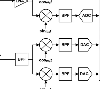
The recent level of increased integration of both analog and digital systems on a single chip provides opportunities to implement a complete test setup with minimum support of external tester. This may include both the test stimuli generation and response analysis for device characterization. For example, Figure 1.1 illustrates a block level model of a modern wireless ZIF radio transceiver architecture [2].
8 Introduction
It can be observed that it is a combination of mixed-signal circuits which can be reutilized during test mode to characterize either an individual device or a combination. Moreover, powerful digital-signal processors available in most of the system-on-chip devices can provide sufficient resources to analyze the test response.
Besides the possibilities to avail the opportunities there are challenges associated with the signal BiST. First, the implementation of mixed-signal BiST does not follow specific standards and lacks the robust traceability. Secondly, the use of uncalibrated on-chip analog stimulus and measurement circuit generates doubt into the accuracy of the measurement. Therefore, calibration techniques need to be adopted for analog circuits of mixed-signal BiST [4]. Moreover, the on-chip instrumentation used to implement BiST is usually inferior compared to the available automated test equipment. Finally, the circuit overhead to implement BiST is often overwhelming, unless most of the circuit is already present on chip. Therefore, using BiST for mixed-signal testing is not trivial and requires much more effort to implement a successful test setup on a chip.
1.4
Motivation and Scope of Thesis
The digital built-in-self-test has matured and standardized to a level that is industry-wide acceptable and used most often. With the CMOS technology scaling the digital BiST complements the advanced digital system performance. However, in the case of analog and mixed-signal systems the BiST has not been developed to an extent that enables its usage for high performance mixed-signal/RF circuits. In order to design mixed-signal BiST, which can accurately characterize a device without area overhead and performance compromise of DUT, there is a need to develop understanding of the advantages and limitations of different feasible BiST techniques. Moreover, new architectures and techniques based on clever design approach need to be explored as a viable solution for mixed-signal BiST, which can be adapted for a wide range of high performance circuit applications. Hence, the focus of the thesis is to develop BiST techniques suitable for on-chip test that, in particular, are aimed at stimuli generation for high performance ADCs and RF receiver front-ends.
1.5 Organization of Thesis 9
Specifically, the ADC dynamic test for harmonic and intermodulation distortion can be realized as BiST using the Σ∆ modulation technique implemented in software to encode a single- or two-tone stimulus as a one-bit sequence to generate a spectrally pure signal with a high dynamic range. For this purpose careful frequency planning is proposed to avoid the FFT artifacts for low-pass and band-pass Σ∆ encoding technique. Although, the BP Σ∆ encoding enables high frequency measurements, when the notch frequency goes up the unfiltered portion of the quantization noise tends to decrease SNR which ultimately appears an obstruction for the ADC test in this case. To overcome this drawback a combination of LP and BP Σ∆ modulation is shown useful providing good accuracy for measurements up to the Nyquist frequency.
It has been observed that a possible asymmetry between rise and fall time of one-bit Σ∆ encoded stimulus results in nonlinear distortion and increased noise at low frequencies which hampers harmonic and intermodulation distortion test. In this case, a simple iterative predistortion technique is proposed in the thesis to reduce the low frequency distortion components of stimulus by making use of an on-chip DC calibrated ADC.
On the other hand, the linearity performance of a radio receiver can be characterized using a two-tone RF generator. For this purpose a specialized phase-locked loop architecture is presented in this thesis as a viable solution for on-chip IP3/IP2 test. The PLL provides control over the frequency spacing of two voltage controlled oscillators and a specialized feedback circuit in the PLL is proposed to overcome interference by the reference spurs.
1.5
Organization of Thesis
The thesis is organized into three main parts:
• Part I – Background
• Part II – ADC Dynamic Test
10 Introduction
The Part I begins with Chapter 1, the Introduction, which provides a brief history of testing and a description of conventional test techniques and trends. It also describes possible opportunities and challenges associated with BiST techniques including motivation and scope of the thesis. Chapter 2 includes discussion on VLSI mixed-signal testing in context of CMOS technology, test complexity and RF test.
In Part II, Chapter 3 provides background of static and dynamic performance of ADC. It also addresses the DSP-based measurements and a concept of the digital bit-stream stimulus. The feasibility of pulse width modulated (PWM) one-bit stimulus for dynamic ADC testing is investigated in Chapter 4 along with simulation results. The Σ∆ encoded stimulus is discussed in Chapter 5, which includes the derivation of dynamic range in terms of the modulator order and FFT length. The chapter also addresses the frequency test plan and a concept of combined LP and BP Σ∆ modulation along with simulation results. Stimulus correction is described in Chapter 6 including the derivation of spurious component cancellation and buffer characterization. The technique is verified by simulation results. Finally, Chapter 7 provides the summary on stimulus generation for ADC dynamic test.
The Part III starts with Chapter 8 providing the background of nonlinear distortion. It also addresses the importance of two-tone test and IP3/IP2 specifications for different receiver front-ends. Next, a two-tone generator is discussed in general including the details of the component blocks, the linear adder to generate the desired stimulus and voltage controlled oscillator. Then the phase noise and injection locking is explored in a context of two-tone operation. Finally, the phase lock-loop issues are discussed which are critical for a possible implementation. The two-tone generator is proposed in Chapter 9 in two variants of PLL architecture followed by the implementation along with the simulation results and discussion. Chapter 10 provides the summary of the two-tone RF generator. The future work is addressed in Chapter 11.
1.6 References 11
1.6
References
[1] K. B. Schaub and J. Kelly, Production Testing of RF and System-on-a-Chip Devices for Wireless Communications, Artech House Inc., 2004. [2] J. Kelly and M. Engelhardt, Advanced Production Testing of RF, SoC, and
SiP Devices, Artech House Inc., 2007.
[3] K. Gray, “Current trends in test-handler technology,” Evaluation Engineering, vol. 36, no. 5, 1997.
[4] M. Burns and G. W. Gordon, An Introduction to Mixed-Signal IC Test and Measurement, Oxford University Press, 2001.
Chapter 2
VLSI Mixed-Signal Testing
2.1
Introduction
One or two decades ago an application/test engineer would have been performing specific tests on discrete analog, mixed-signal and digital components which were ultimately assembled on a printed circuit board for a given system design. Today, the semiconductor industry faces an increased level of CMOS integration such that many of these high performance analog and digital circuits are used as building blocks constituting a standalone system on chip [1]. As a result, testing becomes a complex problem as well and has to be planned in advance, that is, during the circuit design. Hence, the need of design-for-testability techniques (DfT) or built-in-self-test (BiST) for mixed-signal/RF circuits has become necessary as well. Even though on-chip testability comes at the expense of extra silicon area and much design effort, in mass production the cheap CMOS technology comes along with this choice in favor of the guaranteed product quality. Moreover, the manufacturing spread in
14 VLSI Mixed-Signal Testing
contemporary submicron CMOS processes calls for on-chip calibration techniques, which come along with test as well.
2.2
CMOS Technology
The semiconductor industry has been growing at a tremendous pace in the last two decades primarily due to the very large scale integration capability of CMOS manufacturing process [2]. The incursion of CMOS technology in various applications including telecommunication, computing, and different consumer products continues which is likely to carry on for sometime. The primary reason for the CMOS technology to be the choice for vast majority of applications is its relatively simple, inexpensive manufacturing process, integration capability and low power consumption.
The recent development in information technology products is enabled by the possibility to design and manufacture complex systems on a single monolithic integrated circuit. This growth is sustained by the semiconductor industry over a significant period of time by providing high performance products at substantially low cost. Although, scaling of transistor provide the opportunity of large scale integration of systems, a number of technical challenges limits the continuation of the Moore’s Law [3]. The difficulty in design and manufacturing of sub-micron CMOS process has increased to a level where utilization of its full potential seems to be unrealistic. For example, the increased leakage current in complex integrated circuits could be a cause of long term readability concerns.
Similarly, the nominal operation of a scaled transistor is highly susceptible to natural manufacturing process spread. This is particularly critical for analog and mixed-signal circuits integrated on the same die. Unlike digital circuits which in a case of fault or defect may not generate the correct logic, the mixed-signal components my still be functional but might not fulfill the desired specifications and hence degrade the overall performance of the system.
2.3 Test Complexity 15
2.3
Test Complexity
As the complexity of modern high performance integrated circuits has increased the application of a comprehensive test to characterize the complete system is becoming rather expensive in terms of test resources and time. Even if it is possible to perform the complete functional test for the digital part of the system, poor specifications of uncharacterized mixed-signal circuits may lead to the overall deteriorated performance of the system on chip. This suggests that the mixed-signal circuits should be characterized individually while the digital systems must be tested separately, which consequently increases the test cost and time. Complete functional testing of digital systems is usually prohibited by the number of test vectors and the time. The test time may become even longer if the integrated circuit contains sequential logic.
For a moment let us assume that it is possible to perform both mixed-signal and digital test for a given integrated circuit having a huge number of transistors. This circuit may require a large number of pads and pins to enable the complete characterization and test. Figure 2.1 illustrates the packaging complexity from test point of view. The number of transistors on a chip continues to double every 1.5 to 2.0 years [2]. However, the number of pins grows at an annual rate of approximately 11 % [4]. The bigger integrated circuits typically require a large number of pads and pins to enable data flow and adequate power and noise immunity. For such large systems approximately two-third of all pads are dedicated to the power supply and ground to deliver in excess of 100 W power. On the other hand, in high performance application specific integrated circuits (ASICs) approximately half of the total number of pads is used for power and ground. Therefore, with increased integration, the depth of DUT that is to be accessed from primary pins increases and the test controllability and observability becomes more and more difficult externally. In this case newer test techniques need to be developed which can effectively increase test yield and reduce the test cost and time.
16 VLSI Mixed-Signal Testing
Figure 2.1 Number of transistor per I/O pin for microprocessor and ASICs [4].
2.4
Mixed-Signal/RF Test
The integration of RF circuits onto the chip already containing high performance digital and mixed-signal circuits have pushed the traditional test systems to their limits and in most cases they are no longer capable to test these devices. Although, numerous test systems are available from different vendors with varying degree of capabilities, the RF-only tester topology is disappearing primarily due to high cost associated with these systems [5]. The analog and digital functionality along with RF subsystems on a chip needs new testing capabilities to be incorporated into the automated test equipment. Moreover, the challenge of measuring the frequency response of wideband RF and mixed-signal devices increases the technical complexity and cost of the testers as well
2.5 References 17
as the test time. This pushes the need for DfT and BiST to be implemented on a chip both for device characterization and production testing.
2.5
References
[1] K. B. Schaub and J. Kelly, Production Testing of RF and System-on-a-Chip Devices for Wireless Communications, Artech House Inc., 2004. [2] M. Sachdev and J. Pineda de Gyvez, Defect-Oriented Testing for
Nano-Metric CMOS VLSI Circuits, 2nd Edition, Springer, 2007.
[3] G. Moore, “Cramming more components into integrated circuits,” Electronics, vol. 38, no. 8, 1965.
[4] International Technology Roadmap for Semiconductors [Online], Available http://public.itrs.net
[5] J. Kelly and M. Engelhardt, Advanced Production Testing of RF, SoC, and SiP Devices, Artech House Inc., 2007.
Part II
Chapter 3
Background
3.1
Intoduction
The first vacuum tube high performance general purpose data converter became available in mid-1950s pioneered by Bernard M. Gordon [1]. In 1960s the interest in ADCs rapidly increased due to advancements in solid state circuits and mainframe computers. Early applications for data converters were instrumentations, PCM and radar applications. At that time there was no direct way to measure the frequency domain performance of sampling ADCs due to lack of large memory and digital computers to handle the data [2]. By the mid-1970s the mini-computers made possible the dynamic testing of ADCs using FFT [3]. The IEEE-488 bus was used to transfer the ADC samples to the computer for analysis. During 1980s the requirement of ADC testing grew due to demanding applications such as communication systems, and the manufacturers started to specify and include the ADC dynamic performance in converter data sheets [4]. The earlier standards used for digital video and waveform generators were latter updated to include the terminology and test
22 Background
methods for ADCs [5]. By 1990s the frequency domain testing of low speed ADCs become a normal practice with the readily available computers and FFT implementations. Although, today almost all ADCs are fully characterized for AC performance, the testing of high speed and high resolution ADCs for RF applications is still a challenge.
3.2
Static Test Limitations
In addition to the frequency domain testing, conventional static or DC testing is still used to partially characterize ADCs for the following specifications.
1) DC gain and offset error
2) Integral and differential non-linearity (INL and DNL) 3) Monotonicity and missing code
The static test can be carried out using either back-to-back test, crossplot test, servo-loop test or, histogram test [2]. However, based on the stimulus requirements and test setup limitations none of these methods can be adopted for the on-chip ADC test. For example the back-to-back static test setup requires precision ramp generator and a DAC with N+2 bits to test N-bit ADC. The crossplot test also requires a precision ramp generator and a DAC to adjust the DC offset of stimulus. The integrating servo-loop implementation is limited by inadequate precision of analog integrator, while the digital (DSP) based servo-loop test requires a high resolution DAC. Finally, the most widely adopted histogram (code density) test requires precision sinusoidal or linear triangular waveform generator. The other limitation of these ADC test methods is that no information can be extracted for the conversion and recovery time, effect of sampling frequency, aperture jitter, and sparkling. Moreover, as the frequencies and conversion rate increases the transmission parameters become more important for testing than the intrinsic parameters of ADC under test [6].
3.3 Dynamic Performance 23
3.3
Dynamic Performance
In contrast to static testing, a typical high resolution ADC for RF applications can be fully specified in terms of standard dynamic specifications [2] such as
1) Signal to noise ratio (SNR)
2) Signal to noise and distortion ratio (SNDR) 3) Harmonic distortion (HD)
4) Spurious free dynamic range (SFDR)
4) Second- and third-order intermodulation distortion (IMD) and, 5) Effective number of bits (ENOB).
The SNR which is the ratio of RMS signal amplitude to the mean value of root-sum-square of all other spectral components except the first five harmonics and DC, can be measured using a single-tone stimulus. The best possible SNR in dB for an ideal N-bit Nyquist-rate ADC can be expressed as:
SNR = 6.02N + 1.76 dB (3.1)
while in case of over-sampling ADC, it can be expressed as:
SNR = 6.02N + 1.76 dB + 10log(OSR) dB (3.2) where OSR is the over sampling ratio expressed as OSR = fS/(2f0) for a sampling
24 Background
Figure 3.2 Spurious free dynamic range of an ADC.
frequency fS and fundamental frequency f0 [7]. The SNR of a typical N-point
FFT is depicted in Figure 3.1 [2]. In this case the FFT processing gain is a function of N, that is, increasing the number of samples reduces the noise floor to measure the RMS quantization noise of ADC and hence SNR. The SNDR which represents the overall dynamic performance and is the ratio of RMS signal amplitude to the mean value of root-sum-square of all other spectral components including harmonics but without DC, can be measured in a similar way. The SNDR can also be converted to ENOB using the theoretical SNR of an N-bit Nyquist-rate ADC as
ENOB = (SNDR – 1.76 dB)/6.02. (3.3)
For high speed ADCs designed for RF applications the most important specification is the spurious free dynamic range shown in Figure 3.2. SFDR is defined as the ratio of the RMS signal amplitude to the RMS value of the peak spurious spectral component (measured over the Nyquist band).
The non-linearity of a wide-band ADC can be characterized using a single-tone stimulus to measure harmonic distortion within the bandwidth of ADC under test. The HD is the ratio of power of fundamental tone to the sum of powers of the harmonics. If there is a non-linearity in the transfer function the harmonics at multiple of input frequency can be measured by computing the
3.3 Dynamic Performance 25 M a g n it u d e ( d B )
Figure 3.3 Harmonics due to non-linearity.
M a g n it u d e ( d B )
Figure 3.4 Intermodulation products due to non-linearity.
FFT of output. If careful frequency planning is not carried out before the test, the higher order harmonics may fall within the measurement band due to aliasing as shown in Figure 3.3 [8]. On the other hand if the frequency response of ADC is band limited, such as in case of Σ∆ converter, a two-tone stimulus can be used to measure the second- and third-order intermodulation products of
26 Background
Figure 3.5 Back-to-back and envelope & beat frequency setup for ADC testing.
ADC [9]. For two tones at frequency f1 and f2, the second-order IM product
appears at f2± f1 while the third-order IM products appear in particular at 2f1– f2
and 2f2– f1 as shown in Figure 3.4. In this case also, careful frequency planning
is vital for correct measurements. The IM products can be measured in the same way using FFT to estimate the second- and third-intercept point, IP2 and IP3 respectively.
In order to perform the dynamic test of an ADC, ideally a distortion free single- or two-tone sinusoidal signal with accurate and preferably adjustable amplitude is required as test stimulus. Then the frequency domain characteristics of ADC can be analyzed by using coherent DSP-based FFT measurements.
For off-chip measurements, the dynamic performance of ADCs can be evaluated using high-end instrumentation such as automated test equipment (ATE) using conventional back-to-back test or the envelope and beat frequency test setup as shown in Figure 3.5 [2]. However, for test implemented on-chip the generation of distortion free stimulus and the requirement of N+2 bit DAC impose impractical constraints. Although the FFT computation and measurement can be carried out using on-chip DSP resources, the essential bottleneck for on-chip test is the generation of spectrally pure high frequency and high SNR stimulus.
3.4 DSP-Based Measurements 27
3.4
DSP-Based Measurements
In a context of dynamic test of ADC which is essentially based on FFT, coherent sampling is vital. If this criteria is not fulfilled the energy of the fundamental and its harmonics leaks into the adjacent frequency bins of FFT [2]. Additionally if there exists a strong correlation between the input stimulus and quantization noise of the ADC under test, the quantization noise may appear concentrated at various harmonics of input stimulus [6]. Therefore in order to avoid the FFT leakage and artifacts of quantization noise correlation, the unit test period (UTP) must have an integer number of cycles of the input signal (M0)
and an integer number of sampling intervals (MS), where M0 and MS must be
mutually prime. In coherent sampling the sampled UTP repeats itself periodically. The coherence in terms of input frequency f0 and the sampling
frequency fS can be defined as
f0/fS = M0/MS . (3.4)
An additional benefit of coherent sampling in DSP-based testing for multi-tone stimulus is that the test stimulus is composed of two or more mutually orthogonal sinusoidal components. In the response they are statistically independent with zero correlation [6]. This implies that the individual components of signal, distortion and noise can be separated and measured accurately. Also, for HD and IM measurements the likelihood that one or more components fall in the same FFT bin is minimized if the input frequencies are prime multiples. Finally, the implementation of digitally encoded stimulus [10] in terms of UTP can easily be accomplished using system clock and dividers to set M0/MS ratio and ensure coherent sampling for an on-chip test.
Together with the coherent sampling the following rules for tone pruning also improves the test accuracy [6]:
1) Remove all even multiples in multi-tone wideband stimulus to avoid conflicts with second-order harmonics and intermodulation products. 2) Remove all multiples divisible by three in multi-tone wideband stimulus. 3) Select multiples of stimulus tones frequencies that are relatively prime. 4) Select odd multiples in a multi-tone narrowband stimulus to ensure enough
28 Background SNR = 6.02n + 1.76 dB = 74 dB n = 12-bit N = 4096 RMS Signal Level (FS) RMS Quantization Level FFT Noise Floor Frequency M a g n it u d e ( d B ) 10log(N/2) = 33 dB fs/2 0 74 107
Figure 3.6 Effect of FFT processing gain on SNR measurement.
If it is not possible to use coherent sampling for the test setup, FFT windowing function must be used to avoid the leakage of energy of the fundamental tones and its harmonics. In this case the correct spectral resolution of the respective windowing function must be used in the measurement computation. For example, the spectral resolution for Hann window is 3fS/(2N)
instead of fS/(2N) for N-point FFT.
For correct frequency domain measurements it is also necessary to apply corrections for FFT processing gain. In the output spectrum the FFT noise floor may not correspond to the expected SNR of ADC under test. For example in the case of 12-bit Nyquist-rate ADC the theoretical SNR is 74 dB. However, the theoretical noise floor for N-point FFT is 10log(N/2) dB below the quantization noise due to processing gain of the FFT. For example, N=4096 would result in a processing gain of 10log(4096/2) = 33 dB which results in the FFT noise floor of 74 + 33 = 107 dBfs as shown in Figure 3.6 [9]. In fact, the FFT noise floor can further be reduced by increasing the number of FFT samples for weak HD and IM measurement products which might otherwise be buried in the RMS quantization noise floor.
Another important aspect to be considered for DSP-based test is the DNL of ADC transfer function. For a practical ADC, the DNL is usually spread across
3.5 Digital Bit-Stream Stimulus 29
the entire transfer curve of ADC. In this case the distortion components in the output spectrum reflect the INL. However, for reduced input amplitude the harmonic distortion due to DNL does not generally decrease for reduced signal amplitude [9].
3.5
Digital Bit-Stream Stimulus
In a standard production test setup for ADC the stimulus is generated off-chip by specialized instrumentation such as mixed-signal ATE [11]. The frequency response is analyzed by FFT using DSP-based ATE spectrum analyzer or other high-end instrumentation. In this case, typically the stimulus is guaranteed to be spectrally clean with adjustable frequency and amplitude. However, with increased complexity of the contemporary mixed-signal integrated circuits (ICs) and the higher demand for complete system-on-chip (SoC), the off-chip test is becoming more cumbersome and costly. Production test techniques using test access points are often limited by chip performance, operating frequency, and cost of the test instrumentation. For this reason design-for-testability (DfT) and built-in-self-test (BiST) techniques for mixed-signal ICs have been around for the last decade. Based on the concept of reusability a test setup can be realized by incorporating some of the on-chip resources with minimal add-on circuitry. Additionally, with the advent of embedded DSP processors the mixed-signal/RF BiST on a chip has become viable. However, as mentioned before, practical implementation of a precise analog signal generator on a chip for test is still a challenge.
Analog test stimuli can be generated on-chip using two conventional techniques [12]. The first is based on purely analog circuits such as ramp generators [13], or Colpitts/Wien-Bridge to generate a single- or multi-tone signal. Although various analog waveform generators have been reported in the literature [14] which can be used for mixed-signal test, the stimulus integrity of such BiST circuits is limited in terms of amplitude and harmonic distortion requirements, especially in the case of high resolution ADC test. For example, testing a 14-bit ADC requires at least 18-bit linear signal that in case of BiST means on-chip generation of highly linear and undistorted stimuli resulting in impractical design requirements.
30 Background
The second approach is based on a digital signal which is generated as a bit steam sequence and then converted by a digital-to-analog converter (DAC) or by an analog reconstruction filter to generate the analog stimulus. One such a variant is a pseudo-random noise generator derived from digital linear feedback shift registers (LFSRs) [15]. In this case the digital bits are composed of known amplitude tones spread out uniformly across the Nyquist band. For a specific test the out-of-band tones can be removed using an analog low-pass filter. However, the approach is not robust since the power spectral density after low pass filtering is dependent on the filter and is prone to process variations [12]. Other implementations include either a DAC to generate the stimulus or use DSP to determine the characteristic parameters of ADC under test. Digital generators do not need calibration but calibration of the multi-bit DAC is vital for the desired precision of stimulus. Similarly, in a case of the on-chip filter the stimulus characteristics could be sensitive to the type or order of the filter which is also prone to the process variations.
In a context of ADC testing, unlike the classical analog approach to generate stimulus, if a one-bit digitally encoded single- or multi-tone bit-steam [16] is used directly as test stimulus with sufficient dynamic range then the test setup is very much simplified and all non-idealities of DAC and/or filter, essentially, can be avoided. In this case, however, it is assumed that the filter is present on DUT, such as for low-pass Σ∆ ADC. On the other hand if the bit-steam is encoded in such a way that the stimulus characteristics (distortion and quantization noise) become independent of the reconstruction filter, a high precision stimulus can be generated. In this way the filter type, order and sensitivity to cut-off frequency as well as process variations do not impose strict requirements for the generation and implementation of a test stimulus.
These approaches have two key advantages. Firstly, on-chip digital resources can be reused to store and generate a periodic bit-stream and, if required a simple first- or second-order analog filter can be implemented on-chip saving significant silicon area. Secondly, the precision of such a stimulus is relatively high compared to all-analog and DAC based digital implementation. Moreover, a high frequency resolution is achievable with programmability. However, the
3.6 References 31
design of such an encoded stimulus is not straightforward and has limitations in terms of the measurement dynamic range and clock frequency.
3.6
References
[1] B. M. Gordon, “Definition of accuracy of voltage to digital converters,” Instruments and Control Systems, May 1959, pp. 710.
[2] W. Kester, D. Sheingold, The Data Conversion Handbook, Analog Devices Inc., Chapter 5: Testing Data Converters.
[3] B. Pratt, “Test A/D converters digitally,” Electronic Design, Dec. 6, 1975. [4] T. Wilhelm, “Test A/D converters quickly and efficiently,” Electronic
Design, Oct. 15, 1981, pp. 193-198.
[5] IEEE Std. 1241-2000, IEEE Standard for Terminology and Test Methods for Analog-to-Digital Converters, IEEE, 2001.
[6] M. L. Bushnell, V. D. Agrawal, Essentials of Electronic Testing for Digital Memory & Mixed-Signal VLSI Circuits, Kluwer Academic Pub., 2004.
[7] D. A. Johns, K. Martin, Analog Integrated Circuits, John Wiley & Sons Inc., 1997.
[8] M. F. Toner, G. W. Roberts, “A frequency response, harmonic distortion, and intermodulation test for BIST of sigma-delta ADC,” IEEE Trans. On Circuits and Systems-II, vol. 43, no. 8, Aug. 1996.
[9] Analog Devices Inc., Mixed-Signal and DSP Design Techniques, compiled by Walt Kester, 2000.
32 Background
[10] M. M. Hafed, G. W. Roberts, “Techniques for high-frequency integrated test and measurement,” IEEE Trans. on Instrumentation and Measurement, vol. 52, no. 6, Dec. 2003, pp. 1780-86.
[11] J. Kelly and M. Engelhardt, Advanced Production testing of RF, SoC, and SiP Devices, Artech House Inc., 2007.
[12] B. Dufort, G. W. Roberts, “On-chip analog signal generator for mixed-signal built-in self-test,” IEEE J. of Solid-State Circuits, vol. 34, no. 3, pp. 318-330, March 1999.
[13] B. Provost, E. Sanchez-Sinecio, “On-chip ramp generators for mixed-signal BIST and ADC self-test,” IEEE J. of Solid-State Circuits, vol. 38, no. 2, pp. 263-273, Feb. 2003.
[14] G.W. Roberts and A.K. Lu, Analog Signal Generation for Built-In Self-Test of Mixed-Signal Integrated Circuits, Kluwer Academic Publishers, 1995.
[15] E. Liu, C. Wong, Q. Shami, S. Mohapatra, R. Landy, P. Sheldon, and G. Woodward, “Complete mixed-signal building blocks for single-chip GSM baseband processing,” in Proc. IEEE 1998 Custom Integrated Circuits Conf., Santa Clara, CA, May 1998, pp. 101-104.
[16] M. M. Hafed, N. Abaskharoun, G.W. Roberts, “A 4-GHz effective sample rate integrated test core for analog and mixed signal circuits,” IEEE J. Solid-State Circuits, vol. 37, no. 4, April 2002, pp.499-514.
Chapter 4
Pulse Width Modulated Stimuli
4.1
Introduction
In general, the test of high-resolution and high-speed ADCs specifically designed for RF receivers and embedded in a system on chip is not only critical but also a challenging task. The dynamic test addressing various specifications like SNR, SFDR and, INL and DNL in terms of harmonic and intermodulation distortions, for such high speed ADCs require a measurement setup which provides precise test stimuli and can handle large data sets. In a standard approach this implies a need for expensive test equipment and usually long test time. Obviously, the BiST is an option but the test quality requirements make it a real challenge. For example, testing a N-bit ADC requires at least N+4 bit highly linear and undistorted stimuli resulting in tough design constraints. Specifically, the dynamic performance of an ADC is generally characterized by FFT of the output response to a spectrally pure single-tone or two-tone stimulus. Although techniques to test the high resolution ADCs using either the mixed-signal automated test equipment or specialized hardware based on FPGA are
34 Pulse Width Modulated Stimuli
catching up the technological advancements, generation of a test stimulus which is accurate enough, spectrally clean in terms of SNR and HD within a specified bandwidth is still a bottleneck.
Recently, a fully digital approach to generate a test stimulus by pulse width modulation (PWM) used for high resolution ADCs has been reported with a focus on static test [1]. The advantage of this technique is that a 1-bit data pulse train can convey the wanted test signal without harmonic distortions that is particularly attractive for on-chip test. This is in contrast to the true analog techniques or DAC based techniques implemented on a chip, where the spectral purity of the generated signals can be difficult to guarantee.
Although the PWM technique to generate a digitally encoded stimulus is attractive, careful investigation in terms of the ADC dynamic test such as SNR and HD measurements needs to be carried out. For example it is important to pay attention to the spectral content of the PWM stimuli which tends to hamper HD and SNR test and because of this it needs filtering. Also the FFT specifications are critical for the dynamic test. It is also necessary to address the effect of coherent sampling and the FFT processing gain on SNR and spurious free dynamic range.
In order to evaluate the feasibility of PWM for on-chip test the discussion in this chapter is arranged as follows [2]. Firstly, the PWM technique is characterized in terms of the requirements for ADC dynamic test. Then the PWM measurements by FFT technique are discussed. To validate the results, simulation results of a multi-bit Σ∆ ADC under SNR and HD test are presented afterwards. Conclusions are provided in the last section at the end.
4.2
PWM Stimulus Requirements
In order to test an ADC with a large effective number of bits, ideally a distortion free sinusoidal tone with accurate amplitude should be applied as the test signal. Although different BiST techniques have been reported in the literature none of them has gained significant adoption for ADC test, specifically for RF applications. PWM technique can be used to overcome the accuracy problems typical of analog implementations, especially the nonlinear distortions. In this case a limiting factor is pulse-width precision which is reflected by SNR
![Figure 2.1 Number of transistor per I/O pin for microprocessor and ASICs [4]](https://thumb-eu.123doks.com/thumbv2/5dokorg/5428374.139955/40.892.179.719.219.602/figure-number-transistor-i-o-pin-microprocessor-asics.webp)


