Dissertations, No 1716
Techniques for Efficient
Implementation of FIR and
Particle Filtering
Syed Asad Alam
Division of Computer Engineering
Department of Electrical Engineering
Linköping University
SE–581 83 Linköping, Sweden
Dissertations, No 1716
Syed Asad Alam
syed.asad.alam@liu.se www.da.isy.liu.se/
Division of Computer Engineering Department of Electrical Engineering Linköping University
SE–581 83 Linköping, Sweden
Copyright c 2016 Syed Asad Alam, unless otherwise noted. All rights reserved.
Alam, Syed Asad
Techniques for Efficient Implementation of FIR and Particle Fil-tering
ISBN 978-91-7685-915-5 ISSN 0345-7524
Typeset with LATEX
Finite-length impulse response (FIR) filters occupy a central place many signal processing applications which either alter the shape, frequency or the sampling frequency of the signal. FIR filters are used because of their stability and pos-sibility to have linear-phase but require a high filter order to achieve the same magnitude specifications as compared to infinite impulse response (IIR) filters. Depending on the size of the required transition bandwidth the filter order can range from tens to hundreds to even thousands. Since the implementation of the filters in digital domain requires multipliers and adders, high filter orders translate to a large number of these arithmetic units for its implementation. Research towards reducing the complexity of FIR filters has been going on for decades and the techniques used can be roughly divided into two categories; reduction in the number of multipliers and simplification of the multiplier im-plementation.
One technique to reduce the number of multipliers is to use cascaded sub-filters with lower complexity to achieve the desired specification, known as frequency-response masking (FRM). One of the sub-filters is a upsampled model filter whose band edges are an integer multiple, termed as the period
L, of the target filter’s band edges. Other sub-filters may include complement
and masking filters which filter different parts of the spectrum to achieve the desired response. From an implementation point-of-view, time-multiplexing is beneficial because generally the allowable maximum clock frequency supported by the current state-of-the-art semiconductor technology does not correspond to the application bound sample rate. A combination of these two techniques plays a significant role towards efficient implementation of FIR filters. Part of the work presented in this dissertation is architectures for time-multiplexed FRM filters that benefit from the inherent sparsity of the periodic model filters.
These time-multiplexed FRM filters not only reduce the number of multi-pliers but lowers the memory usage. Although the FRM technique requires a higher number delay elements, it results in fewer memories and more energy effi-cient memory schemes when time-multiplexed. Different memory arrangements and memory access schemes have also been discussed and compared in terms of their efficiency when using both single and dual-port memories. An efficient
pipelining scheme has been proposed which reduces the number of pipelining reg-isters while achieving similar clock frequencies. The single optimal point where the number of multiplications is minimum for non-time-multiplexed FRM filters is shown to become a function of both the period, L and time-multiplexing fac-tor, M . This means that the minimum number of multipliers does not always correspond to the minimum number of multiplications which also increases the flexibility of implementation. These filters are shown to achieve power reduction between 23% and 68% for the considered examples.
To simplify the multiplier, alternate number systems like the logarithmic number system (LNS) have been used to implement FIR filters, which reduces the multiplications to additions. FIR filters are realized by directly designing them using integer linear programming (ILP) in the LNS domain in the minimax sense using finite word length constraints. The branch and bound algorithm, a typical algorithm to implement ILP problems, is implemented based on LNS integers and several branching strategies are proposed and evaluated. The filter coefficients thus obtained are compared with the traditional finite word length coefficients obtained in the linear domain. It is shown that LNS FIR filters provide a better approximation error compared to a standard FIR filter for a given coefficient word length.
FIR filters also offer an opportunity in complexity reduction by implement-ing the multipliers usimplement-ing Booth or standard high-radix multiplication. Both of these multiplication schemes generate pre-computed multiples of the multipli-cand which are then selected based on the encoded bits of the multiplier. In transposed direct form (TDF) FIR filters, one input data is multiplied with a number of coefficients and complexity can be reduced by sharing the pre-computation of the multiplies of the input data for all multiplications. Part of this work includes a systematic and unified approach to the design of such computation sharing multipliers and a comparison of the two forms of multipli-cation. It also gives closed form expressions for the cost of different parts of multiplication and gives an overview of various ways to implement the select unit with respect to the design of multiplexers.
Particle filters are used to solve problems that require estimation of a system. Improved resampling schemes for reducing the latency of the resampling stage is proposed which uses a pre-fetch technique to reduce the latency between 50% to 95% dependent on the number of pre-fetches. Generalized division-free architectures and compact memory structures are also proposed that map to different resampling algorithms and also help in reducing the complexity of the multinomial resampling algorithm and reduce the number of memories required by up to 50%.
Sammanfattning
Digitala filter är signalbehandlingsalgoritmer som används i många olika typer av applikationer och system. Som i de flesta fall finns det ett generellt intresse att göra saker enklare och effektivare. I denna avhandlingen studeras två olika klasser av filter och förbättringar föreslås för effektivare implementering av dessa filter.
Den första klassen av filter är så kallade FIR filter. Dessa kräver typiskt många operationer när det finns strikta krav på filtreringen. Då multiplikatio-ner är klart mer komplexa än additiomultiplikatio-ner, både var gäller area, tid och effektför-brukning, så fokuseras arbetet på dessa. Traditionellt finns det två spår för att förbättre detta: antingen minskar man antalet multiplikationer eller så förenklar man multiplikationerna. Metoder för bägge områdena föreslås i detta arbetet.
Ett effektivt sätt att konstruera FIR filter med väldigt smalt övergångsband, dvs avståndet mellan frekvenser som släpps igenom och som dämpas, är att an-vända frekvensmaskning. I denna typen av filter så använder man ett filter där många av multiplikationerna är noll och därmed inte behöver beräknas. Detta filter har nollorna fördelade i ett periodiskt mönster vilket leder till att bete-endet i frekvensdomänen också blir periodiskt. Fördelen är att komplexiteten för att skapa ett väldigt smalt övergångsband skalar omvänt proportionellt med perioden, så ju högre period desto lägre komplexitet. Då det oftast inte är ett pe-riodiskt filter man vill ha i slutänden så behövs det ytterligare filter som tar bort de oönskade delarna i frekvensdomänen. Dessa har typiskt högre komplexitet för högre period, så en lagom avvägning måste hittas.
Trots mycket tidigare arbete på att konstruera sådana filter har väldigt lite arbete lagts på att implementera dem effektivt. Här har vi speciellt tittat på fallet där datatakten, som bestäms av applikationen, och kretsens klockfrekvens, som bestäms av implementeringsteknologin, inte är samma. Specifikt det mest realistiska fallet att datatakten är lägre än klockfrekvensen. En arktitektur som tar hänsyn till det periodiska filtret har föreslagits och olika möjligheter har utretts i detalj. Resultaten visar att vid implementering på en FPGA så mins-kar mängden minne som används, tvärtemot vad man kan tro. Ett ytterligare resultat är att effekten minskar ca 80% av minskningen i antal multiplikationer.
Ett alternativ för att minska komplexiteten på multiplikationerna är att använda logaritmiska talsystem (LNS). I dessa blir multiplikationerna bara en addition av exponenterna. I detta sammanhanget har för första gången optima-la filter konstruerats direkt i den logaritmiska domänen med ändlig ordlängd. Att kunna konstruera optimala filter i både den linjära och logaritmiska domä-nen är en förutsättning för att kunna göra korrekta jämförelser mellan filter implementerade i de bägge domänerna.
Ytterligare ett alternativ för att minska komplexiteten på multiplikationer-na är att använda multiplikatorer med högre radix och dela vissa delar mellan flera multiplikatorer. Vid implementering av FIR filter uppkommer ett mycket gynnsamt fall för detta. I avhandlingen föreslår vi ett enhetligt sätt att konstru-era och utvärdkonstru-era denna typ av multiplikatorer. På så sätt visar vi att tidigare arbeten bara var specialfall av denna generella metod. Då tidigare arbeten inte visat hur parametrar valt eller i vissa fall ej ens insett kopplingen till multipli-katorer med högre radix, kan vi visa hur man bör välja parametrar för bästa effektivitet.
Till sist behandlas en helt annan typ av digitala filter. Dessa så kallade parti-kelfilter används för att skatta tillstånd i dynamiska system. Den kritiska delen för effektiv implementering här är omsamplingssteget. Vi förslår tre metoder för att förbättra implementeringen av detta. En direkt implementering av omsamp-ling bygger på att man jämför innehållet i två minnen. Varje cykel läser man från ett av minnena, vilket beroende på resultatet av tidigare jämförelse. Den förbättrade metoden bygger på att man läser in extra data från det ena minnet och kan på så sätt utföra den total jämförelsen snabbare. Med bara ett extra jämförelseblock kan man statistiskt minska den kritiska tiden med 56%. Den andra metoden löser problemet med att normalisering av värdena som jämförs, vilket normalt kräver en division. Istället används enbart multiplikationer och som en bieffekt så kan vi även skapa sekvenser av sorterade slumptal på ett nytt effektivt sätt. Till sist visar vi att upp till hälften av minnet som används för att spara sekvenserna som ska jämföras kan sparas genom att beräkna resultaten i real-tid.
Praise be to Al-Mighty Allah, the most Compassionate, the most Merciful, who gave me an opportunity to contribute to the vast body of knowledge. Peace and blessings of Allah be upon the Holy Prophet Muhammad (Peace be upon Him), the last Prophet of Allah, who has always exhorted his followers to seek knowledge and whose life is the glorious model for the humanity.
There are a lot of people to whom I would like to express my gratitude. The following is certainly not exhaustive but an effort to thank those who had the most impact on my research and life in Linköping:
• My advisor, Dr. Oscar Gustafsson, for having confidence in me by giving me an opportunity to complete my PhD. I am greatly indebted to him for his inspiring and valuable guidance, enlightening discussions, his pa-tience when ever I was short of his standards and constant encouragement in difficult times, kind and dynamic supervision through out and in all the phases of this thesis. Working and learning from him was always a pleasure. Thank you Oscar.
• My co-supervisor, Dr. Kent Palmkvist, for help with FPGA, VHDL and Linux related issues.
• The former and present colleagues at the old Division of Electronics Sys-tems, Department of Electrical Engineering, Linköping University for cre-ating a very friendly environment. They always were kind enough to do their best to help you.
• The former and present colleagues at the Division of Computer Engi-neering, Department of Electrical EngiEngi-neering, Linköping University for making me feel welcome when I joined their division and helping out when needed.
• A special thanks to our current and past secretary Gunnel Hässler and Susanna von Sehlen for helping out in various administrative tasks. • A special thanks to Doktorand Syed Ahmed Aamir for his support, both
materialistic and spiritual, during my early days in Linköping which im-mensely helped me in settling in this city.
• My present and former room-mates, Dr. Fahad Qureshi, Doktorand Carl Ingemarsson and Doktorand Fahim-ul-Haque for putting up with me,
building a good working environment and having discussions on mundane and technical issues.
• Dr. Muhammad Abbas for his help and guidance at the start of my PhD studies.
• Doktorand Muhammad Touqir Pasha and Doktorand Fahim-ul-Haque for proof reading and giving valuable advice while I was writing my thesis. • Dr. Fahad Qazi, Doktorand Muhammad Touqir Pasha, Dr. Jawad ul
Has-san, Dr. Hafiz Muhammad Sohail, Dr. Nadeem Afzal, Dr. Irfan Kazim, Dr. Usman Dastageer, Dr. Muhammad Junaid and others for building a nice social circle without which it would have been hard for me and my family to live here.
• Finally a special thanks to my family
– My mother, Tanweer Alam, for her immense love, sacrifices, guid-ance, support and upbringing. Without her I would not be where I am. Without her life means nothing to me. It was on her encour-agement that I took the decision to pursue PhD even though living so far apart was always troubling for her. Thanks Maa, because without your prayers and support, I would not have been able to complete my studies.
– My wife, Eyshaa Zehra, you have been a true life partner, bearing the load of taking care of home and children while I spent long hours in office, for always showing love, patience, affection to me and for your immense support and cooperation. You made taking a lot of tough decisions easy for me.
– A special thanks to my children, Muhammad and Arwaa, whom I am sure will read this when they grow up, for taking away all the tiredness and stress with their beautiful smiles, small giggles and playful gestures while welcoming me home.
– My whole extended family in Pakistan, Canada and the U.S.A, my in-laws, my aunts and uncles, my cousins etc., for always being there for me and for making me feel special.
• To those not listed here, I say profound thanks for bringing pleasant moments in my life.
Syed Asad Alam, January 21, 2016, Linköping Sweden.
2C Two’s complement
ASIC Application specific integrated circuit ASIP Application specific instruction set processor BILP Binary integer linear programming
BLE Basic logic element BMI Brain machine interface CFGLUT Configurable LUT CLB Configurable logic block CPA Carry propagate adder
CPLD Complex programmable logic device CPU Central processing unit
CSA Carry save adder CSD Canonic signed digit
CSE Common subexpression elimination CU Control unit
DA Distributed arithmetic DAG Directed acyclic adder graphs DF Direct form
DFT Discrete fourier transform DSP Digital signal processing
EEPROM Electrically erasable programmable read only memory EPROM Electrically programmable read only memory
FF Flip flop
FFA Fast FIR
FFT Fast fourier transform FIFO First in first out
FIR Finite-length impulse response FPGA Field programmable gate array FRM Frequency-response masking FSM Finite state machine
GPC Generalized parallel counter GPU Graphical processing unit HDL Hardware description language HMM Hidden Markov model
HPM High performance multiplier IC Integrated circuit
ICAP Internal configuration access port IDFT Inverse DFT
IFIR Interpolated FIR
IIR Infinite impulse response ILP Integer linear programming
IMHA Independent Metropolis Hastings algorithm LNS Logarithmic number system
LP Linear programming LSB Least significant bit LUT Look-up table MAC Multiply-accumulate
MC Monte Carlo
MCM Multiple constant multiplication MILP Mixed integer linear programming MPGA Mask programmable gate array MSB Most significant bit
MSD Minimal signed digit MSE Mean square error
NP Non-deterministic polynomial OPR Overlapped partial resampling PAL Programmable array logic PAG Pipelined adder graph PE Processing element PLA Programmable logic array PLD Programmable logic device PMCM Pipelined MCM
PROM Programmable read only memory RCA Ripple-carry adder
RNA Resampling with nonproportional allocation RNS Residue number system
RPA Resampling with proportional allocation RPAG Reduced pipelined adder graph
RSG Reduced slice graph
RSR Residual systematic resampling RTL Register transfer level
S-ASIC Structured ASIC
SCM Single constant multiplication SD Signed digit
SEU Single-event upset
SIMD Single instruction multiple data SIS Sequential importance sampling SM Signed magnitude
SMC Sequential Monte Carlo SPT Signed power of two
SRAM Static random access memory SSF Single stage FIR
STM State transition model TDF Transposed direct form TID Total ionizing dose
ulp Unit of least significant position VLSI Very large scale integrated
I
Background
1
1 Introduction 3
1.1 Motivation . . . 3
1.1.1 Reduction in Number of Multipliers . . . 4
1.1.2 Reduction in Multiplier Complexity . . . 5
1.1.3 Improved Particle Filter Resampling Architectures . . . . 7
1.2 List of Publications . . . 7
1.2.1 Other Publications . . . 8
1.3 Thesis Organization . . . 8
2 Implementation Aspects of DSP Algorithms 11 2.1 Introduction . . . 11
2.2 Implementation Platforms . . . 12
2.2.1 Application Specific Integrated Circuits . . . 13
2.2.2 Field Programmable Gate Arrays . . . 15
2.3 Key Arithmetic Operators in DSP Implementations . . . 25
2.3.1 Adders . . . 25
2.3.2 Multipliers . . . 32
2.3.3 Multiple Constant Multiplication . . . 38
2.4 Number Systems . . . 43
3 Finite-length Impulse Response Filters 47 3.1 Introduction . . . 47
3.2 Impulse Response of FIR Filters . . . 47
3.3 Linear Phase FIR Filters . . . 48
3.4 FIR Filters: Input and Output Relationship . . . 49
3.5 FIR Filter Structures . . . 49
3.6 Design of FIR Filters . . . 51
3.6.1 Error Approximation . . . 52
3.6.2 FIR Filter Design by Optimization . . . 53
3.6.3 Remez/Park-McClellan FIR Filter Design . . . 53
3.6.4 FIR Filter Design by Linear Programming . . . 53 xv
3.6.5 FIR Filter Design by Cascade of Sub-Filters . . . 56
3.6.6 Sparse FIR Filter Design . . . 63
3.7 Fast FIR Filters . . . 64
3.8 FIR Filter using Alternate Number Systems . . . 69
3.8.1 FIR Filter using Logarithmic Number System . . . 69
3.8.2 FIR Filter using Residue Number System . . . 70
4 Particle Filters 73 4.1 Introduction . . . 73
4.2 Mathematical Formulation . . . 74
4.3 Particle Filtering Steps . . . 75
4.3.1 Time-Update . . . 76
4.3.2 Measurement-Update . . . 76
4.3.3 Resampling in Particle Filters . . . 76
5 Summary and Future Work 85 5.1 Summary . . . 85
5.2 Future Work . . . 86
References 89 References . . . 89
II
Publications
111
A On the Implementation of Time-Multiplexed Frequency-Response Masking Filters 113 1 Introduction . . . 1162 Frequency-Response Masking Filters . . . 118
3 Design Considerations for Implementing Filters . . . 119
4 Proposed Architecture . . . 120
4.1 Memory Management . . . 121
4.2 Type of Memory . . . 123
4.3 Timing of Read and Write . . . 125
4.4 Pipelining . . . 126
4.5 Architecture – Narrow-Band FRM Filters . . . 129
4.6 Architecture – Wide-Band FRM Filters . . . 130
4.7 Architecture – Arbitrary-Band FRM Filters . . . 130
5 Results . . . 131
5.1 Proposed Model Filter and IP based Model Filter . . . . 131
5.2 Comparison between FRM Techniques . . . 131
5.3 Effect of Time-Multiplexing . . . 133
5.4 Dual-Port Memories and Single-Port Memories . . . 136
5.6 Proposed Architecture vs. Single Stage FIR (SSF) Filter
IP . . . 137
5.7 ASIC Implementation . . . 141
6 Conclusion . . . 141
References . . . 144
B Design of Finite Word Length Linear-Phase FIR Filters in the Logarithmic Number System Domain 147 1 Introduction . . . 150
2 The Logarithmic Number System (LNS) . . . 151
2.1 Finite Word Length Effects . . . 152
3 Proposed Integer Linear Programming Design in the LNS Domain153 3.1 Integer Linear Programming . . . 153
3.2 Linear Programming Design of FIR Filters . . . 154
3.3 ILP Design of FIR Filters in the LNS Domain . . . 155
4 Results . . . 157
4.1 Comparison of Branching Schemes . . . 157
4.2 Effect of Word Length . . . 161
4.3 Changing the Base . . . 163
5 Conclusion . . . 165
References . . . 168
C A Unified Approach to the Design and Implementation of Com-putation Sharing Multipliers 171 1 Introduction . . . 174
2 Multiplication . . . 175
2.1 Standard High-Radix Multiplication . . . 176
2.2 Booth Algorithm . . . 176 3 Cost Models . . . 178 3.1 Pre-Computer . . . 178 3.2 Select Unit . . . 178 3.3 Encoder . . . 183 3.4 Summation . . . 183
4 Computation Sharing Multipliers . . . 185
5 Results . . . 186
5.1 Single Multiplier . . . 187
5.2 Tri-State Buffer Based Multiplexer . . . 192
5.3 Transposed Direct Form FIR Filters . . . 193
5.4 Complex Multipliers . . . 195
6 Conclusion . . . 197
D Improved Particle Filter Resampling Architectures 203
1 Introduction . . . 206
2 Architectures for Particle Filters . . . 207
3 Resampling in Particle Filters . . . 210
4 Proposed Techniques . . . 214
4.1 Reduction in Resampling Latency – Pre-Fetch . . . 214
4.2 Generalized, Division-Free Resampling Architecture . . . 218
5 Results . . . 221
5.1 Latency Reduction . . . 221
5.2 Memory Usage by Generalized Division-Free Architecture for Multinomial Resampling . . . 225
6 Conclusion . . . 226
Introduction
The topic of this thesis is techniques for efficient implementation of finite-length
impulse response (FIR) and particle filtering. It encompasses four different
contributions towards fulfilling the requirements of this thesis:
• Proposing an architecture for the implementation of time-multiplexed frequency-response masking (FRM) filters and analyzing different mem-ory organization and access schemes involved in this architecture. • Design of FIR filters by optimizing the filter coefficients in the logarithmic
number system (LNS) domain
• Analysis and unified design of different computation sharing multiplica-tion schemes and their applicamultiplica-tions to complexity reducmultiplica-tion in FIR filters • Proposing a scheme and corresponding architecture for the reduction in the latency of the resampling stage of the particle filter, a generalized division-free architecture and compact memory structure for its imple-mentation
This chapter aims to introduce these research topics and motivate their rele-vancy in modern day applications. It also presents all the research publications that have resulted as part of the research work done and the thesis organization.
1.1
Motivation
FIR filters are one of the most widely used filters and have played a leading role in frequency selective digital filtering since its inception [1–4]. They are inherently stable and free of limit cycle oscillations caused by using finite word length as long as they are not implemented in a recursive manner. They can be easily designed to be linear phase and hence achieve constant group delay, which helps in preserving the integrity of the information carrying signals and is crucial in communication signals [5].
However, FIR filters suffer from a major disadvantage as they require a higher order to achieve narrow transition bands as compared to infinite impulse response (IIR) filters. This results in more arithmetic operations like multipliers and adders and also an increase in the number of delay elements. Since the filter order of an FIR filter is inversely proportional to the transition band-width, any decrease in band-width increases the computational complexity of the FIR filters significantly [3].
Due to this high computational complexity of FIR filters, research has been on going for decades to reduce it [3, 6]. The proposed techniques to reduce the computational complexity can be broadly divided with respect to the optimiza-tion goals; reducoptimiza-tion in the number of multipliers [7–27] and reducoptimiza-tion in the multiplier complexity [28–42]. The contributions of this thesis are towards both research fronts.
Another topic covered in this thesis the resampling step of particle filtering. The execution of the resampling step is a bottleneck as it cannot be executed in parallel with the other steps in the particle filtering. Furthermore, the multi-nomial resampling algorithm suffers from high computational cost because its implementation requires a search through two large sequence of numbers and their normalization. A number of resampling algorithms has been proposed that deals with the parallelism problem [43, 44] but none has been proposed that reduces the computational cost of multinomial resampling algorithm. Fur-thermore, the bottleneck remains in the implementation of traditional resam-pling algorithms [45]. The work presented in this thesis proposes solutions to reduce the latency which can be used to increase the parallelism and reduce the computational cost of multinomial resampling.
1.1.1
Reduction in Number of Multipliers
A common approach to reduce the number of multipliers is to realize the fil-ter through the cascade of sub-filfil-ters. These sub-filfil-ters can either be differ-ent [46–51] or iddiffer-entical [13, 52–55]. The main premise of these techniques is that by the use of sub-filters, less stringent requirement with regards to tran-sition bandwidth will be placed on these sub-filters, thus reducing the number of distinct multipliers at the cost of an increased order. The non-identical sub-filter technique uses building blocks having different powers of z−1. The
identical sub-filter technique using identical building blocks and connects them with the aid of additional adders and multipliers [54]. One of the most popular techniques utilizing different powers of z−1 is the FRM technique [48]. These
techniques achieve a reduction in the number of multiplications by making use of a combination of wide transition-band filters generally termed as model filters and masking filters. The model filter is first upsampled by L by the insertion of L − 1 zeros between every coefficient, resulting in a filter called the periodic model filter, which compresses the spectrum of the filter to form the desired transition band of the target filter but produces images. The images are then filtered or masked out by the masking filters. The non-identical sub-filters can
be combined in different ways to either produce arbitrary, narrow or wide-band filters. For narrow-band FIR filters, when the pass-band is less than π/2, the overall filter structure can be further reduced to just one periodic model and one masking filter [46, 47, 50]. From this narrow-band structure, efficient wide-band structure can also be derived by the use complementary filter while the technique of using identical sub-filters with different up-sampling factors have also been proposed to synthesize narrow and wide-band FRM filters [13].
The design of FRM filters have received considerable attention but only a few attempts have been made towards the dedicated implementation of these filters [14, 16, 22, 24, 56–58]. Furthermore, since contemporary state-of-the-art implementation platforms like application specific integrated circuit (ASIC) or field programmable gate array (FPGA) allow the circuits to be clocked at hundreds of MHz upto a few GHz and only rarely do the sampling rate require-ments of DSP systems correspond to these high frequencies, time-multiplexed architectures are crucial. These architecture re-use different resources thereby reducing the number of such resources. Since typically FRM filters have more delay elements than a single-stage implementation of FIR filters, it is necessary to study what affects time-multiplexing has on not only the number of multi-pliers but also on the mapping of these delay elements to memories. Paper A presents contributions towards the implementation of time-multiplexed FRM filter where different memory organizations, access schemes, affect of pipelining on these schemes and the effect of time-multiplexing on the optimal value of L which gives the minimum number of multipliers are analyzed.
1.1.2
Reduction in Multiplier Complexity
The other method to reduce the complexity in FIR filters is to reduce the complexity of the multipliers. There are different methods to do this and can be broadly divided into three categories
1. Single/multiple constant multiplication 2. Number representation
3. Computation sharing
These three techniques can be combined in different ways to further optimize the multiplications and can also be combined with the techniques outlined in Section 1.1.1 [32, 59–61].
Single constant multiplication refers to the optimization of the filter coeffi-cients in the signed power of two (SPT) space [62, 63] because each coefficient can be represented as a sum of a limited number of SPT terms. The multipli-cation of each coefficient with the input data can either be implemented as a general multiplier or by using a fixed shift-add network because typically the filter coefficients are constant. The number of adders in a shift-add network is primarily determined by the number of non-zero terms in the representa-tion of a filter coefficient and a reducrepresenta-tion of these non-zero terms is what is referred to as reduction or minimization in the number of SPT terms and
in-teger linear programming (ILP) has been a popular technique to achieve this minimization [62, 64–70].
Further reduction can be achieved by combining single constant multiplica-tion (SCM) with across multiple constants, known as multiple constant multi-plication (MCM). MCM is applicable to the transposed direct form (TDF) FIR filter whose operation can be modeled as an MCM problem [38]. The reduction in the number of adders is achieved by extracting common subexpressions within a filter coefficient and across multiple coefficients. The techniques proposed for MCM can be broadly divided into two categories, common subexpression elim-ination (CSE) [71] and the adder graph technique [28].
The CSE technique is based on pattern matching techniques and the result depends on the initial representation of the filter coefficients where typically canonic signed digit (CSD) is used as the number representation [29, 30, 72–74]. This is because CSD number representation has only around 33% non-zero digits relative to the word length as compared to 2′s complement number
represen-tation which has approximately 66%. These techniques have been combined with integer or mixed integer linear programming [6, 60, 62, 70, 71, 75–78] and minimum spanning trees [31, 33, 79] to yield even better results in terms of number of additions required to realize these coefficients.
The adder graph technique is value based and independent of the underlying number representation [71]. Here partial sums are symbolically represented in the nodes of the graph while the edges are used to represent the shift amounts [28]
Furthermore, different number representations have been used to take advan-tage of the inherent simplification of multiplication in them, like residue number system (RNS) [80–84] and LNS [85–92]. Most efforts towards utilizing LNS for digital filters have focused on either implementing the non-linear conversion to and from LNS, selecting the logarithm basis, or implementing the LNS addition and subtraction efficiently [92–97]. The finite word length filter design has not been considered, but instead relied on rounding the obtained coefficients to the nearest LNS number.
Paper B presents the contribution in this area where an integer linear pro-gramming (ILP) approach to design optimal finite word length linear-phase FIR filters in the LNS domain is proposed. Here, instead of optimizing filters in the linear domain and converting them into LNS with rounding in the LNS, the filter is directly optimized in the minmax sense in the LNS domain with finite word length constraints.
Another source of reducing the multiplication complexity is by sharing some parts of the actual computation when Booth [98–101] or high-radix multipli-cation [102] is used. A number of proposed techniques have used alphabets to pre-compute multiples of the multiplicand to be selected based on multi-plier bits and shared this pre-computer for all multiplications in the TDF FIR filter [103–109]. However, this approach is a special case of high-radix multipli-cation when the radix is 16. Similar sharing can also be performed with Booth
multiplication and in Paper C the attempt is made to analyze both of these mul-tiplications with respect to computation sharing. Furthermore, different design choices have been discussed that are available while designing different parts of the multiplier.
1.1.3
Improved Particle Filter Resampling Architectures
The final contribution of this thesis is the proposal of efficient architectures for the resampling step in particle filtering. In particle filters a weighted set of particles is propagated that approximates the probability density of the un-known state conditioned on the observations. This is achieved by the recursive generation of random measures which are composed of particles drawn from relevant distributions and of importance weights of the particles [110, 111]. Par-ticle filters find application in a wide variety of complex problems including target tracking, computer vision, robotics and channel estimation in digital communication or any application involving large, sequentially evolving data-sets [112–115].Among the three steps that accomplish particle filtering, resampling is the most crucial to obtain an efficient implementation of the estimation. It presents a bottleneck in that this step of resampling cannot be executed in parallel with other steps. A number of research work have focused on different resampling algorithms [43, 44, 116–121]. However, these contributions do not discuss the multinomial resampling which is the most basic form of the resampling step. The current work in Paper D looks into improving different aspects of the re-sampling stage. The first technique proposed is the proposal of a generalized division free architecture and compact memory structure which helps in com-plexity of the multinomial resampling algorithm. In addition to this, a technique has been proposed to reduce the latency of the resampling stage along with the required hardware details.
1.2
List of Publications
This thesis contains research work done between March 2010 and January 2016, and has resulted in the following publications.
Paper A
• S. A. Alam, and O. Gustafsson, “On the implementation of time-multiple-xed frequency-response masking filters,” IEEE Trans. Signal Process., under second review.
Preliminary versions of the above work have been published in
• S. A. Alam and O. Gustafsson, “Implementation of time-multiplexed sparse periodic FIR filters for FRM on FPGAs,” in Proc. IEEE
Inter-national Symposium on Circuits and Systems (ISCAS), Rio de Janeiro,
• S. A. Alam and O. Gustafsson, “Implementation of narrow-band frequen-cy-response masking for efficient narrow transition band FIR filters on FPGAs,” in Proc. NORCHIP, Lund, Sweden, Nov. 14–15, 2011.
Paper B
• S. A. Alam, and O. Gustafsson, “Design of finite word length linear-phase FIR Filters in the logarithmic number system domain,” VLSI Design, vol. 2014, Article ID 217495, 14 pages, 2014.
Paper C
• S. A. Alam, and O. Gustafsson, “A unified approach to the design and implementation of computation sharing multipliers,” Manuscript.
Paper D
• S. A. Alam, and O. Gustafsson, “Improved particle filter resampling ar-chitectures,” IEEE Trans. Signal Process., under review.
A preliminary version of the above work has been published in
• S. A. Alam and O. Gustafsson, “Generalized division-free architecture and compact memory structure for resampling in particle filters,” in Proc.
Europ. Conf. Circuit Theory Design (ECCTD), Trondheim, Norway,
Aug. 24–26, 2015.
1.2.1
Other Publications
Contributions have also been made in the following publication but the contents are not relevant to the topic of this thesis.
• F. Qureshi, S. A. Alam and O. Gustafsson, “4k-point FFT algorithms based on optimized twiddle factor multiplication for FPGAs ,” in Proc.
IEEE Asia Pacific Postgraduate Research on Microelectron. Electron.,
Shanghai, China, Sept.22–24, 2010, pp. 225–228.
1.3
Thesis Organization
The thesis is organized in two parts. The first part establishes the background of the work. It outlines and summarizes the previous research work that has been done in the related field and how this work has brought forward the re-search front. The second part contains the collection of the rere-search publications outlined above.
The first part of the thesis is organized in five chapters. Chapter 2 out-lines various areas connected with the implementation of digital signal process-ing (DSP) algorithms. Specifically it divides these areas into thee distinct fields, (a) implementation platforms, (b) arithmetic operations and (c) number systems. The two main platforms discussed in this chapter are ASIC and FPGA. It has
been shown that the way these platforms are utilized for implementing DSP al-gorithms, their key features and their differences. It moves on to describing the key arithmetic operations involved in the implementation, i.e., adders, multipli-ers and number systems used to represent data and their effect on the overall performance of DSP algorithms.
In Chapter 3, a backround of FIR filters is presented. Advantages and chal-lenges involved in the use of FIR filters is highlighted. To meet these chalchal-lenges, a number of techniques have been proposed to design and optimize FIR filters with respect to its computation complexity and this chapter attempts to high-light key areas important towards the reduction in the implementation cost of FIR filters.
An overview of the particle filter algorithm with special focus on the re-sampling step is presented in Chapter 4. Different algorithms to implement the resampling step is discussed in this chapter while also highlighting different hardware architectures presented in various works.
Finally, Chapter 5 concludes the background part and presents future chal-lenges in the considered work.
Implementation Aspects of
Digital Signal Processing
Algorithms
2.1
Introduction
The design and synthesis of a DSP algorithm, based on a set of specifications, is the first step towards the realization of the complete DSP system. The second step is the mapping of the algorithm to a set of hardware resources like memories, processing elements (PEs), control and interconnection network. The connec-tion between these four fundamental elements is shown in Fig. 2.1. The two most important operations of these PEs, specially for implementation of DSP algorithms, are the adder and multiplier. The memory also has an important role to play in the implementation of these algorithms [122]. The third and the final step is the implementation of these resources on some hardware platform which require the data to be represented using finite word length based on some number system.
The organization of this chapter is as follows: in Section 2.2, various hard-ware platforms available are described along with their main features, advan-tages and drawbacks. Furthermore an overview of the two primary arithmetic operators involved in DSP algorithms, the adder and the multiplier is presented in Section 2.3. Number representation plays an important role in the imple-mentation of DSP systems and affects the overall performance and cost of im-plementing them. A brief overview of different number systems is presented in Section 2.4.
Communication
Memory Processing
elements
Control
Figure 2.1: Hardware resources. Redrawn with permission from [122].
2.2
Implementation Platforms
For real world applications, all algorithms need to be implemented on some kind of hardware platform. With the growing trend of very large scale inte-grated (VLSI) designs, a number of platforms are available. Each of these platforms have different levels of programmability. The platform with the high-est degree of programmability is the general purpose micro-processors such as Intel R
Core R
processors. On the other hand, dedicated hardware accelerators, which have a fixed functionality occupy the other end of the spectrum of de-vices. In general, all implementation platforms can be categorized under ASICs because every platform is associated with a specific application, only the granu-larity is different. In terms of integrated circuit (IC) fabrication technologies, an IC can be classified as full-custom, semi-custom and programmable ICs [123].
The full custom IC is a layout-based technique where the circuit is drawn manually at the transistor level. Highest layout efficiency and maximum circuit performance is achieved at the cost of high initial design effort. These circuits and layouts are collected in libraries together with automatic generation to form
mega-cells, for e.g., state-of-the-art micro-processor cores.
However, such an effort is not necessary for majority of applications. To achieve the required performance in these applications, circuits can be composed of pre-designed cells. These cells are made up of elementary logic gates and stor-age elements. These cells are automatically placed and routed using dedicated layout strategies. These techniques take the form of either standard-cell, gate-array/sea-of-gates and FPGA. The design of circuits targeting this level of ab-straction is generally carried out using hardware description languages (HDLs) like Verilog or VHDL. Using these languages, the circuit may be described at the behavioral level, register transfer level (RTL) level or structural level.
Standard-cells are themselves a full-custom design while gate-arrays/sea-of-gates consist of preprocessed wafers with predefined but unconnected transistors. Only the metallization is customized which defines the interconnect between the transistors and is often called an mask programmable gate array (MPGA) [124]. In FPGAs, an array of logic blocks and routing channels are configured or programmed using a configuration stored in a static memory. Generally, in the wider electronics engineering community, standard-cell based layout is referred
to as an ASIC and this terminology will also be used here.
Another implementation platform, called structured ASIC (S-ASIC), mar-ries the benefits of FPGAs and ASICs in terms of cost, capabilities, turn around time and ease of design [125]. S-ASICs typically contain prefabricated elements which either implements generic logic (called a tile) or special logic like con-figurable I/O, microprocessor cores, embedded memories and others [125]. An-other key differentiator of S-ASIC is the availability of prefabricated metal layers and the design only needs to specify a few metallization layers to complete the device.
From a functionality point of view, a central processing unit (CPU) is only used for general purpose processing. For computation intensive tasks, the main work load is transferred to hardware accelerators. These hardware accelerators can again be programmable, for e.g., a graphical processing unit (GPU) or fixed, for e.g., ASIC [126]. From a signal processing point of view, instead of using a CPU, there is a need to use a more specific processor which is flexible yet not very generic like a CPU. This need is filled by either a digital signal processors (DSPs) or application specific instruction set processors (ASIPs) [127].
DSPs and ASICs occupy the two ends of the spectrum of platforms used to implement DSP algorithms. DSPs are flexible but slow and power hungry while ASICs are non-flexible but very fast and power efficient. FPGAs fill the gap between these two extreme ends. They provide a flexibility not achievable in an ASIC while being faster and consume less power than a DSP [128, 129].
Here the focus will be on standard-cell based ASICs which is described in some detail, in Section 2.2.1 while FPGAs find their description in Section 2.2.2.
2.2.1
Application Specific Integrated Circuits
A standard-cell based ASIC, referred to as an ASIC here, uses pre-designed standard cells, like logic gates (AND, OR, etc.), multiplexers, flip flop, half and full adders and tri-state buffers, to implement a system.
These cells, arranged as rows, may also be combined with megacells like mi-crocontrollers, microprocessors and memories. These standard cells are placed by the ASIC designer who also defines the interconnect. These standard cells are constructed using full-custom design methods and their use allow the same performance and flexibility as a full-custom ASIC but reduces design time and risk. However, all the mask layers of an ASIC are unique and customized for a particular design.
An ASIC vendor provides all cells in a library called a standard cell library. Each cell in a library contains the following
• A physical layout • A behavioral model
• A Verilog and/or VHDL model • A detailed timing model • A test strategy
Design Synthesis System partitioning Floorplanning Placement Routing
Figure 2.2: ASIC design flow [124].
• A cell icon (symbol) • A wire-load model • A routing model
The behavioral model is needed for simulation while the timing model is required to determine the performance of an ASIC. Wire-load models are used to estimate the parasitic capacitance of wires. Circuit schematic and cell icon is used in schematic based design entry.
A ASIC Design Flow
The ASIC design flow is divided into a number of steps, as shown in Fig. 2.2. System partitioning can be done before the design steps and there may be iterations between the different steps. The design entry is typically made using an HDL while synthesis translates the HDL description into gates.
System partitioning is used to divide a system into multiple sub-systems while floorplanning is used to estimate the physical sizes and set the initial relative location of the various blocks. The location of clock- and power networks and that of the input/output pins are decided in the same stage. The location of the logic cells is defined in the placement step while setting aside space for the interconnect and finally routing makes the connections between the logic cells.
B Implementation of Adders and Multipliers on ASICs
Typically, the standard cell library has four main types of cells [124]. These are combinational, sequential, data-path and I/O cells. Each of these cells come with different drive strengths, power specification, capacitance and delay at different temperatures, supply voltages and threshold voltages (VT).
Combinational cells range from simple inverter, AND, OR, NAND cells to more complex cells which contain a comhination of different cells. Cells for efficiently implementing multiplexers, transmission gates and tri-state buffers are also a part of the combination cell library. Sequential cells typically contain
different types of latches and flip-flops. In addition to the different properties mentioned above, they are also available with different timing constraints like pulse width, hold and setup times. Cells for scan-based flip-flops which are useful for data-path scanning used in testing of VLSI circuits are also available.
As mentioned earlier, the primary arithmetic operators used in DSP algo-rithms are adders and multipliers. Cells that implement them are part of the data-path cells [124]. Data-path cells also implement operations that use multi-ple signals across a data bus. Full-adder and half-adder cells are typically part of any standard library. They are available with different delays between inputs and outputs, specially between carry-in and carry-out as it is part of the carry chain. However, it is not necessary that these cells are used in the actual imple-mentation, specially if there are tighter timing constraints or logic surrounding the adder operation, which is typically the case. The synthesizer may well use other cells or optimize the logic to implement it more efficiently.
In multiplication, the partial product generation stage will use different types of combinational cells. Depending on the timing and area constraints and how the design has been entered using any of the HDLs, summation of the partial products may be implemented using either summation trees or array adders. Key components of these summation structures is typically the carry-save adder which avoids carry-propagation of the ripple-carry adder. Other elements that can be synthesized using data-path cells are multi-input NAND gates, registers, multi-bit multiplexers, or incrementers/decrementers [124].
2.2.2
Field Programmable Gate Arrays
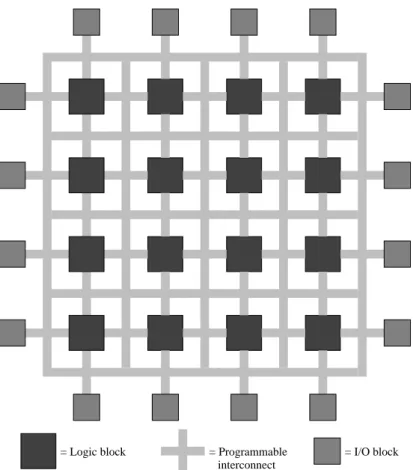
An FPGA is an integrated circuit designed to be configured by the customer or a designer after being manufactured making them programmable. The design entry, similar to that of an ASIC, is typically made using HDLs. Its config-uration is generally specified using an HDL, which is also used for designing ASICs. It significantly reduces the design time while also reducing the proto-typing cost by more than a few decades. FPGAs can be used to implement any logic function, either combinational or sequential. The ability to re-program without going through the whole fabrication cycle of an ASIC provides a sig-nificant advantage, especially for low-volume applications. They can also be reconfigured if a problem is identified [130, 131]. A general architecture of an FPGA consisting of blocks implementing digital logic, interconnect resources and I/O blocks is shown in Fig. 2.3. In more advanced FPGAs, some of the logic blocks are replaced by specialized blocks like memories and multipliers.
A History
The emergence of FPGAs is connected to the emergence of early programmable devices which employed regular architecture and flexible functionality. Earlier types of such devices consisted of cellular and “cutpoint” cellular arrays [132] where the functionality of each logic cell was programmed in the field through
= I/O block = Logic block
interconnect = Programmable
the use of programming currents or photo-conductive exposure [132]. The next device, made available in the 1970s, was the programmable read only memories (PROMs) with its two variants of mask-programmable and fuse-programmable ROMs. However, the area of a PROM is exponentially dependent on the number of address inputs and thus unfeasible for large number of address inputs.
The first programmable device which had a two-level logic structure was the programmable logic array (PLA) which had a fixed AND plane and a pro-grammable OR plane. Sufficient flexibility is provided by a propro-grammable AND followed by a fixed OR plane, giving rise to the programmable array logic (PAL) device [133]. However, in order to implement sequential circuits, registers (flip flops (FFs)) are added to PALs to form a programmable logic device (PLD). Multiple PLDs are placed on a single chip to form a complex programmable logic device (CPLD) where they are connected using programmable routing devices [128].
From these programmable devices emerged the FPGA which not only has multi-level programmable logic but also has programmable interconnect. Dif-ferent claims have been made to the origin of the first FPGA [129, 134–137], however, the first modern era FPGA was introduced by Xilinx in 1984 [135] with devices like XC2064, XC4000 and XC6200. These FPGAs consisted of an array of configurable logic blocks (CLBs) and contained around 64–100 such blocks with 3-input look-up tables (LUTs) and 58 inputs and outputs. With time, the complexity of FPGA has grown to include hundreds of thousands of such blocks in addition to large specialized blocks like memories, multipliers and serial interfaces which has greatly expanded the capability of these devices and laid the foundation of a new technology and market [129, 138–140].
Xilinx continued unchallenged and had a quick growth from 1985 to the mid-1990s, when competitors came up, reducing its market-share significantly. The 1990s were an explosive period of time for the growth FPGAs, both in sophistication and the volume of production. In the early 1990s, FPGAs were primarily used in telecommunications and networking. By the end of the decade, FPGAs found their way into consumer, automotive, and industrial applications [140].
In the first decade of the new century, extremely complex FPGAs were marketed, specially by Xilinx and its main competitor Altera. Platforms like Virtex and Kintex series by Xilinx and Cyclone and Stratix series by Altera enabled designers to implement extremely complex applications on FPGAs.
B FPGA Programming
As shown in Fig. 2.3, the architecture of a FPGA is similar to a MPGA. MPGAs are mask programmable which does not give the same flexibility as the field programmability of FPGA [137]. This programming of FPGAs is done through programmable switches of which there are a number of types. Historically, the approaches that have been used to program FPGA include [128, 129] electri-cally programmable read only memory (EPROM) [141], electrielectri-cally erasable
programmable read only memory (EEPROM) [142, 143], flash [144], static ran-dom access memory (SRAM) [135] and anti-fuses [145]. Of these programming technologies, only the flash (Microsemi, Actel), static memory (Xilinx, Altera, Lattice) and anti-fuse (Actel) are popular in modern FPGAs, depending on the type of applications they are employed for.
Typically, SRAM based FPGA are for more mainstream applications like communication and signal processing while flash is used for low power applica-tions [146, 147]. Anti-fuse FPGAs, meanwhile, find applicaapplica-tions in space appli-cations where they have been shown to be immune to single-event upsets (SEUs) and degrading of the characteristics due to total ionizing dose (TID) [148]. How-ever, anti-fuse FPGAs are only one-time-programmable, a significant drawback from FPGA perspective.
C Basic Building Blocks
The basic building blocks of an FPGA, as shown in Fig. 2.3, consists of the following [128, 129, 137]:
• configurable logic block (CLB) • Programmable interconnect • I/O block
A single FPGA CLB can be as simple as a transistor [149] or as complex as a microprocessor [129]. However, there are inherent problems with either of these two extremes. The kind of fine-grained programmability provided by using transistor as a CLB will entail large amounts of programmable interconnect resulting in poor area efficiency, low performance and high power consumption. On the other end, think of implementing a small adder or multiplier using a microprocessor. The inherent inefficiency is visible illustrating the problems of architectures that are too coarse-grained.
In between the fine and coarse-grained architectures lies a full spectrum of CLB choices that are based on one or more of the following [137]
• NAND gates [150]
• Interconnection of multiplexers [139] • LUTs [135]
• Wide-fanin AND-OR gates [151]
The CLB consisting of a pair of transistors in shown in Fig. 2.4 [149]. Simi-larly, the multiplexer based FPGA from Plessey [137] is shown in Fig. 2.5 [150]. These are the examples of fine-grained CLBs. Coarse-grained blocks include a multiplexer, LUT and wide-fanin gates based CLBs.
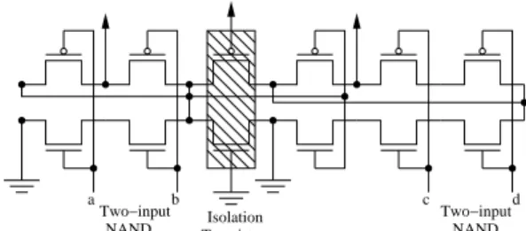
The multiplexer based CLB from Actel, shown in Fig. 2.6 [139, 152], is based on a multiplexer’s ability to implement various logic functions by connecting its input to either some constant value or to a signal [153]. The functionality of a LUT based FPGA is similar to distributed arithmetic (DA) where a LUT is used to implement a truth table [128]. It requires a memory with 2nlocations to implement a n-input function in a LUT. This arrangement is shown in Fig. 2.7 [128]. Typically, a CLB is also used to implement sequential logic thus it will
a b c d f Isolation Transistors Two−input NAND Two−input NAND
Figure 2.4: Transistor based CLB implementing f = ab + c′d′.
Configuration Memory D Q Mux 8 to 2 Interconnection
Figure 2.5: The CLB from Plessey [137] c 1993 IEEE.
have clocked circuits such as flip-flops and latches. A very basic arrangement of this is shown in Fig. 2.8 [128, 129].
The architecture of different types of CLBs shown in these figures are very basic. State-of-the-art FPGAs have very advanced and complex CLBs. One of the earliest FPGAs by Xilinx, the XC3000, had a very complex logic block, illustrated in Fig. 2.9. It contains a 5-input LUT which can also be configured as two 4-input LUTs [129].
As the years progressed, the size of the LUT increased. However, it was important that the effect of this increased size on area and speed is explored. It was shown in [155] that as the LUT size increases, the number of LUTs required to implement the circuit decreases. The cost of this decrease is an increase in the area cost of implementing the logic and routing for each block. A product of these two cost metrics shows that initially there is a decrease in the total area before increasing as LUT size is increased [129].
One alternative way to change this level of granularity is to use multiple LUTs in one CLB, referred to as cluster in [129]. A number of basic logic elements, as the one shown in Fig. 2.8, are grouped together and a local inter-connect structure is used to inter-connect them programmably. This arrangement is shown in Fig. 2.10, which transformed the increase in the logic and routing area from exponential to quadratic [129].
1 0 1 0 1 0 s3 s4 s2 s1 z y x w f
Figure 2.6: Multiplexer based CLB from Actel [137] c 1993 IEEE.
Look−up table configuration bits mux n 1 output inputs 2n
Figure 2.7: LUT based CLB. Redrawn with permission from [128].
D Q Logic
Element
out
Figure 2.8: LUT based CLB with a flip-flop. Redrawn with permission from [128, 129].
D Q R D Q R 5− Input Look−up Logic Variables DI DATA IN X Y Table Enable Clock Clock Reset 0 (Inhibit) (Global Reset) EC K RD
Figure 2.9: CLB of Xilinx XC3000 Series [154].
BLE 1 BLE 1 BLEs N Outputs Inputs Clock
Figure 2.10: BLEs grouped together in a cluster. Redrawn with permission from [129].
Another technique to achieve a better trade-off between larger LUT and cluster sizes is to use clusters of different sized LUTs [156–158]. Different com-binations were realized using this technique achieving a 10% reduction in pin count [156] and 25% improvement in performance [157].
All these technological advances have resulted in current state-of-the-art FPGAs employing a variety of the discussed techniques. The Virtex-7 FPGA provided by Xilinx combines eight LUTs in one CLB by packing four of these in one slice [159]. Its 6-input LUT can also be configured as two separate 5-input LUTs, making the architecture both homogeneous and heterogeneous at the same time. Similary, Altera Stratix II architecture employs a 6-input LUT which can be configured as either one 6-input, two 4-input and a combinatin of 5 and 3-input LUT [160]. These CLBs also contain high-speed carry propagation for arithmetic operations and wide multiplexers and LUTs can also be used to implement memories and shift registers. These memories are commonly referred to as distributed memories because the memory function is distributed across a number of LUTs [159].
D FPGAs for DSP Implementation
High parallelism and throughput requirements of DSP algorithms can be re-alized by specire-alized ASICs. However, as noted earlier, ASICs do not provide high flexibility in terms of reconfigurability [161]. FPGAs on the other hand are inherently built such that they support highly parallel algorithms and provide a higher degree of flexibility in terms of reconfiguration. The introduction of dedicated multipliers and multiply-accumulate units has enabled designers to implement multiplier and multiply-accumulate (MAC) intensive applications in FPGAs. Among the various DSP algorithms, FIR filters are one of the most important algorithms which are widely used in numerous applications. Due to the high amount of MAC operations inherent in an FIR filter, state-of-the-art FPGAs are often used to implement FIR filters [58, 86, 162–169].
Current FPGAs have numerous specialized blocks which map specifically to multiply and MAC operations. These are commonly referred to as DSP blocks. In fact, implementation of digital filters was one of the key factors to push for the inclusion of these DSP blocks in the FPGA fabric [170] which also helped in reducing the performance gap between ASICs and FPGAs.
The DSP block comes in various flavors. The DSP block by Xilinx in their 5, 6 and 7 series FPGAs support various functions, shown in Fig. 2.11. It supports a number of operations, namely a 25 × 18 two’s complement plier, a 48-bit accumulator, a power saving pre-adder, single instruction multi-ple data (SIMD) operation, an optional logic unit, pattern detector, optional pipelining and dedicated buses for cascading DSP blocks (beneficial for FIR filters) and support for wide multiply operations up to 35 × 26 by cascading two DSP blocks [171].
Altera on the other hand has implemented a variable precision DSP block, the basic structure of which is shown in Fig. 2.12. The functionalities supported
A B D C Pattern detector P +/− × +− = 25 × 18
Figure 2.11: Basic structure of a Xilinx DSP slice in series-7 FPGAs [171].
by it are, three 9×9 multipliers, two 18×18 multipliers, one 27×27 multiplier, a 64-bit accumulator and adder, chainout adder for cascading, support for storage of up to eight coefficients storage and a special systolic FIR Mode [172].
The high performance provided by these dedicated DSP blocks have a down-side. The number of DSP blocks available is limited and the word lengths they support are limited. Although Altera provides a variable precision DSP block yet it is still coarse and for applications like video and image processing, which require 8 to 10 bits of resolution, there will be wasted resources if the multipli-cations are mapped to these blocks [173]. Furthermore, if there is a need for large size multiplication, like floating point multiplication with mantissa sizes of 24 and 54 bits, it will require cascading of multiple DSP blocks. This will significantly increase the number of required DSP blocks.
Therefore, there is a need to realize multipliers in the soft logic, i.e., using the programmable CLBs and LUTs for applications where the DSP blocks are not sufficient or the word size does not match the system requirements. For example, a method termed as tiling was introduced in [174, 175]. Here, large multiplications were implemented using several DSP blocks and smaller multi-plications were implemented using the softcore multipliers to “fill gaps” where a DSP block is too large.
A number of techniques have been proposed on the efficient use of the logic elements to implement softcore multipliers. The fast carry chain of modern FPGAs was used to implement a multiplier in [176] which generates the partial products using Booth recoding and adds them using ripple carry adder instead of a compressor tree. To take advantage of 5-input LUTs where two of the outputs can be used independently, the technique proposed in [177] showed that it is possible to generate and compress two partial products of a Baugh-Wooley multiplier [178] which reduces the number of partial products by half, similar to the Booth multiplier. However, there is no decoding/encoding required in a Booth multiplier.
The low level logic of FPGAs have been used to efficiently implement the compressor trees required to add all the partial products. Generalized parallel counters (GPCs) are used to replace the full-adders used in compressor trees
Internal Coefficient
Internal Coefficient
Input register block
Output register block
Chainout adder/ accumulator +/− +/− +/− × × + 18 × 18 18 × 18
Figure 2.12: Basic structure of an Altera DSP slice in stratix-V FPGAs [172].
as a means to reduce the combinatorial delay. Heuristics [179] and ILP formu-lations [180] are proposed for optimizing the delay of compressor trees while also considering the FPGA carry chain for the implementation of GPC [181]. ILP formulations are also proposed for reduced power consumption by reducing not only the depth but also the number of GPCs [182, 183] while efforts to optimize the number of resources for high throughput pipelined designs have been proposed in [184]. In [173], authors present a technique to completely avoid the compressor trees by merging the Booth recoding with the ripple-carry summation of the partial products in a single stage of LUTs, fast carry chains and flip flops. Futhermore, the presence of LUTs in FPGAs makes it attractive for distributed arithmetic based DSP systems [169, 185–189].
Details about multiplication, partial products and compressor trees are pre-sented in Section 2.3.1.
E Reconfigurable DSP Implementation on FPGA
The built-in parallelism of resources in FPGA allows massively parallel appli-cations to be easily implemented in an FPGA. It allows for a high throughput even at low MHz clock rates. This has given birth to a new type of process-ing called reconfigurable processprocess-ing, where FPGAs perform time intensive tasks instead of software [161, 166, 189, 190].
Reconfigurable computing consists of a device, such as an FPGA, performing computations with spatially programmable architectures [191, 192]. It is rapidly establishing itself as a major discipline that inherits a wide body-of-knowledge
from many disciplines including custom hardware design, digital signal pro-cessing, general purpose computing on sequential and multiple processors, and computer aided design.
FPGAs are specially useful for dynamic reconfiguration [192]. It allows for hardware configuration changes during different phases of the computation. Such reconfiguration is important for different systems like communication and networking systems where hardware configurations must change to match pro-tocol needs.
DSP algorithms, specially FIR filters, can also benefit from the reconfigura-bility provided by FPGAs. For applications like multi-stage filters for decima-tion and interpoladecima-tion, polyphase FIR filters [193] or frequency variable filters for telecommunications and digital audio [194], multiplications with constants need to reconfigured from time to time [161].
This reconfiguration can only be achieved in ASICs by low-level multiplex-ing. However, for current FPGAs, there are standard solutions that can provide internal reconfiguration. One is the internal configuration access port (ICAP) of Xilinx FPGAs which allows the logic function as well as the routing to be completely reconfigured during run time. To change the logic only without re-configuring the routing, for example changing the FIR filter coefficients, Xilinx FPGAs provide configurable LUT (CFGLUT). These LUTs can be reconfig-ured in 32 clock cycles by sourcing their contents from block RAM resources resulting in reconfiguration times of the order of 100 ns as compared to the ICAP interface where times are in order of microseconds to milliseconds [161]. These LUTs are similar to standard LUTs but provide a reconfiguration inter-face of data in, data out, clock enable and clock. In [161] and [188], authors have presented reconfigurable FIR filters using LUT based multiplier and distributed arithmetic.
2.3
Key Arithmetic Operators in DSP
Imple-mentations
2.3.1
Adders
Adders perform the most fundamental of all operations in digital signal pro-cessing algorithms. They are used as both standalone operators and as part of operations. Furthermore, they are not only used to add two input operands but can also be used to for multi-operand inputs [123]. From a FIR filter point-of-view, addition appears in two places. First they are needed to add all the partial products generated in a multiplication operation or when a multiplier is realized using a shift-add network. Secondly they appear as structural adders used to add all the products of the multiplication of the filter coefficient with the input data.
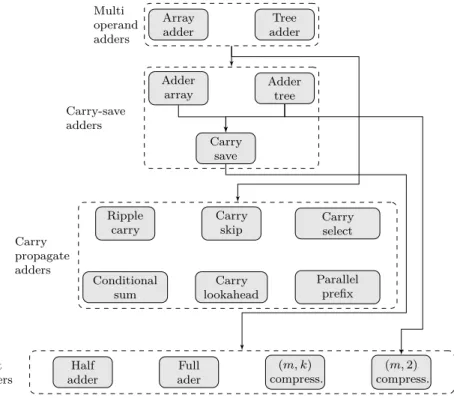
An overview of different adder structures, the relationships and inter depen-dencies is given in Fig.2.13 [123]. Brief descriptions about these structures are
Array adder Tree adder Multi operand adders Adder array Adder tree Carry save Carry-save adders Ripple carry Carry skip Carry select Conditional sum Carry lookahead Parallel prefix Carry propagate adders Half adder Full ader (m, k) compress. (m, 2) compress. 1-bit adders
Figure 2.13: Adder structures and their dependencies. presented later.
A Fundamental Adder Structures
The primary concern with respect to addition is the efficient speed up of the carry propagation. This becomes an even greater concern when adding a number of partial products which typically take the form of multi-operand adders like array-adders or tree-based adders. To improve the carry-propagation a number of adders have been proposed in the literature [123, 195–201]. However, central to all these adders are the 1-bit adder structures which are explained next. Half-Adder, (2, 2) – Counter The half adder has two inputs and two out-puts making it a (2, 2) – counter. It is referred to as a counter because it counts the number of 1’s in the input bits. The two outputs are commonly referred to as the sum and carry out bit with the relationship between the inputs and outputs given by:
2cout+ s = a + b. (2.1)
The resulting truth table resulting from (2.1) is given in Table 2.1. Since a half adder does not have any carry input, its use is rather limited. It finds use in
![Figure 2.1: Hardware resources. Redrawn with permission from [122].](https://thumb-eu.123doks.com/thumbv2/5dokorg/5500369.143241/30.701.214.504.89.218/figure-hardware-resources-redrawn-permission.webp)
![Figure 2.9: CLB of Xilinx XC3000 Series [154].](https://thumb-eu.123doks.com/thumbv2/5dokorg/5500369.143241/39.701.196.521.92.481/figure-clb-of-xilinx-xc-series.webp)
![Figure 2.11: Basic structure of a Xilinx DSP slice in series-7 FPGAs [171].](https://thumb-eu.123doks.com/thumbv2/5dokorg/5500369.143241/41.701.161.539.88.251/figure-basic-structure-xilinx-dsp-slice-series-fpgas.webp)
![Figure 2.12: Basic structure of an Altera DSP slice in stratix-V FPGAs [172].](https://thumb-eu.123doks.com/thumbv2/5dokorg/5500369.143241/42.701.185.530.85.399/figure-basic-structure-altera-dsp-slice-stratix-fpgas.webp)