THE DEVELOPMENT OF THIN-FILM
PHOTOVOLTAIC APPLICATIONS BASED
STRUCTURES ON CUINSE
2WITHIN THE TRIPLE
HELIX MODEL
Vasiliy Rud
Saint-Petersburg state Polytechnic University,
29,Polytechnicheskaya, St.Petersburg,195251, RUSSIA.
e-mail: rudvas.spb@gmail.com
Yury Rud,
Ioffe Physical Technical Institute of Russian Academy of Sciences, St. Petersburg
ABSTRACT
This work concentrates on the rewiew of the study of the photoelectrical phenomena of thin films for solar cells and also show the search of a new physical effects, which may be the basis for the development of new technologies, diagnostic methods, new types of photoconverters, and devices on these multinary semiconductors.Solar cells which based on silicon or binary III– V semiconductor compounds and their solid solutions successfully fulfilled their role as the first energy sources in outer space in the 1950s–1990s. Since 1997, technological development has been carried out for amorphous Si, CdTe thin film polycristal and CuInSe2 (CIS) solar cells in
the thin film solar cell family.
Thin film solar cells based on CuInSe2 and the related materials heretofore have been studied
only for the aims of creating efficiencies. Complex physical and technological studies of the thin film solar cells on the basis chalcogenide chalcopyrite materials have made it possible to create devices with high radiation hardness and efficiencies as high as 18% [1-4].
At the same time, basic studies aimed to speed up film deposition is conducted from the aspect of material and substrate technologies for further cost reductions.
For CIS solar cells research and development efforts continue to establish both element technologies necessary for the improvement in product quality and efficiency and large-area film fabrication technologies as essential part of the solar cell production process.
This study was supported by the contract “Research and Development of Deposition System for CIGS Solar Cell” signed by the Ioffe Physical Technical Institute (Russian Academy of Sciences).
KEYWORDS
CIGS Solar Cell, heterostructures, photoconversion, thin films solar cells (TFSC), solar cells ( SC)
EVAPORATION AND PHOTOCONDUCTIVITY OF CuInSe
2THIN
FILMS
Thin films CuInSe2 have been prepared by evaporation from single source . The starting
stoichiometric CuInSe2 powder has been prepared by direct synthesis of stoichiometric amounts
of the constituent elements was carried out in a closed ampoule by using a Bridgman furnace. In order to check the photoelectrical properties of the films the deposition was made directly on glass substrate [5].
By evaporation from single source we were able to prepare both p- and n-types CuInSe2
films. In order to prepare p-type have been evaporation at the temperature source higher 1150 oC at the temperature substrate T sub = 350 oC. In the narrow region of the temperature source the
films are obtained the transition from p-type to n-type. In this region the films show a high resistivity between 102 - 10 3 Ω ·cm at T= 300 K.
The typical spectral dependences of the steady-state photoconductivity of the obtained thin films as a parameter of the temperature source at constant temperature substrate indicated that the photoabsorption is very sensitive to the temperature of the evaporation.
This results show the new solution of the problems of the control of the fundamental properties of the CuInSe2 films by means of simple modification of the evaporation conditions
without the obtaining of the multinary solid solutions on the basis chalcopyrite semiconductors.
NATURAL PHOTOPLEOCHROISM OF CuInSe
2/ GREEN LEAF
HETEROJUNCTIONS
This proceeds in parallel with unceasing search for new heterojunction components based on CuInSe2 which might reduce the cost of photoconverters, improve their ecological
parameters, and enhance their efficiencies. Some of these studies include natural material and the possibility of getting away from the use of cadmium, which is employed in CuInSe2/CdS
structures and is regarded as an ecologically dangerous element. We have undertaken a study of the possible use of green leaves as a wide band component for heterojunction based on CuInSe2 .
The use of green leaves in photoconverters will obviously solve the ecological and economic aspects of this problem[6-8].
The heterojunctions were fabricated using the single crystals p-CuInSe2 with (001) and
(100) orientation. The heterojunction was created by placing an leaf on a CuInSe2 surface. Thin
films of metal on the glass was used as an transparent ohmic contact on the leaf.
A typical plot of the relative quantum efficiency η of this heterojunction illuminated on the green leaf as a function of photon energy show the shape characteristic of semiconductor heterojunction (Fig. 1). When linearly polarized light acts on heterojunctions of this type the photosensitivity behaves in a way characteristic of a uniaxial medium. The polarization indicatrix of the photocurrent varies periodically. It is important to emphasize that the ratio ip/is
1 ( E║c- ip, E┴c - is ), which suggests that the upper valence band in CuInSe2 has symmetry Г7,
so that the direct A-transitions are predominantly resolved in the E parallel c polarization. The photocurrent polarization indicatrices of this heterojunctions were the same as for CuInSe2 single
The typical spectral dependence of natural photopleochroism for the new type photoconverters have a positive sign and the magnitude of natural photopleochroism are consistent with those for n-p-CuInSe2 homojunctions. The maximum of positive
photopleochroism occurs at the energy of the A-transition, while its value is caused by the tetragonal deformation of CuInSe2 lattice.
These studies, therefore, in the first time show that a contact of CuInSe2 with a green leaf
can be used to create wide band photoconverters for natural and linearly polarized light.
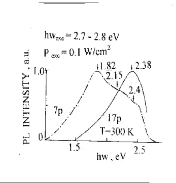
Fig.2. PL spectra of anodized layers on p-CIS bulk crystals (Current density i,mA/cm2 :7p-50,17p-120).
ANODIZED LAYERS ON CuInSe
2BULK CRYSTALS
In this section we report the our results of investigations into the possibility of modifying the emission properties of CuInSe2 by means of well known anodic etching[9-11].
The starting crystals for the anodic etching were electrically homogeneous wafers of CuInSe2 with a free hole concentration 5 x 10 16 cm-3 at T= 300 K. As with similar treatment of
silicon, a diffuse layers was formed on the surface of the starting wafers at the region of contact with the etching and, depending on the etching conditions and the local physical properties, the color of this layer varied between black and white. These layers possessed fairly good adgesion with the substrate.
When the anodized layers were excited by Ar+ - laser radiation we discovered luminescence whose color varied from orange to white-green in different layers and different points of the layer. The typical spectral dependences of the photoluminescence of anodized layers shows that the photoluminescence dominates at photon energies substantially exceeding
Fig. 1. Relative quantum
efficiency spectra of p-CuInSe2/
the band gap of the initial bulk crystals. As in the case of silicon, the photoluminescence spectra are sensitive to the etching conditions. Attention is drawn to the large width at half-maximum of these bands, which indicates that the luminescence centers have a complex structure, incorporating several types of centers, and thus several bands are superimposed.
Thus anodic etching of CuInSe2 crystals produced wide-band gap layers
photoluminescing in the visible range in the form of broad bands. These layers may well find applications as a wide-band gap component to develop optoelectronics devices utilizing CuInSe2
bulk crystals and possible thin films.
POLARIZATION PHOTOSENSITIVITY OF ZnO/CdS/Cu(In,Ga)Se
2THIN
FILM SOLAR CELLS
Thin film solar cells on the basis chalcopyrite thin films have gained increasing interest in the past few years due to the steady progress of conversion efficiencies. The co-evaporation method have already been achieved with the conversion efficiencies of more then 15%. The polarization photosensitivity of such devices has not been investigated yet. Here, we report the main results of an experimental study of the photoelectric properties of a ZnO/CdS/Cu(In,Ga)Se2 thin film solar cells when responding to linearly polarized light, when
opens up a new field of their applications[3,4,12-14].
A typical spectral dependence of the relative quantum efficiency for the heterojunctions in unpolarized light give us a possibility to find out when such devices are illuminated in the direction of the normal to the surface from the side ZnO film, the window effect, typical for such heterojunctions, is observed. In the high efficiency region of the spectrum contains about 7 peaks. The values of the refractive index obtained for different cells lies in the range 1.8 - 2.0 eV, which corresponds to published values for ZnO. The presence of a interference pattern in the efficiency spectra of such heterojunctions is evidently of their high quality.
When the thin film devices illuminated with the linearly polarized light directed along the normal to the ZnO surface, the photocurrent was independent on the orientation of the plane polarization of the incident light throughout the photosensitive spectral region. This independence is attributable to the isotropic nature of the photoactive absorption in the films and to the fact that such an absorption is in turn related to their polycrystalline structure at the absence of a texture. As the angle of incidence becomes nonzero, the photocurrent ip ( E parallel plane of incidence ) over the entire photosensitivity range begins to predominate over the is ( E perpendicular plane of incidence ). As it can be seen from the Figure 4 the angular dependences ip( ) and is( ) for these devices are similar. However, the dependence is( ) turn out to be different then expected from the Freshnel relations. The increase of the photocurrents ip and is in the vicinity of the pseudo-Brewster angles of incidence could be attributed to the suppression of the reflection losses for the both polarization simultaneously. The phenomenon of the enlightenment for the both polarization was observed probably in the high efficiency devices.
A typical angular dependence of induced photopleochroism shows its main distinguishing feature (Fig.3) that with the increasing of the incidence angle the induced photopleochroism
increases according to a nearly quadratic law. The estimated value of the refractive index equally 1.5 - 1.7. It is a lower of known values for ZnO. That may be caused by the interference phenomena. Possibility on this cause the induced photopleochroism begins to vary as a function of the photon energy ( Figure 4). The results presented here thus show that high efficiency thin film solar cells could find on application as wide band photovoltaic converters of natural and linearly polarized light. The observed interference of light in ZnO films indicates that photoelectric polarization spectroscopy could be used for the nondestructive diagnostics of surface quality of thin film photoconverters on the basis of multinary chalcopyrite semiconductors.
.
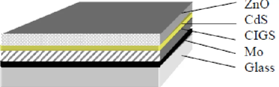
Figure5 shows a schematic CIGS solar cell in a substrate structure and Figure 2 shows a scheme
of CIGS module fabrication process as it is now work [15].
Fig.3. Angle of incidence dependences of the photocurrent ( ip - 1 , is - 2 ) and induced
photopleochroism ( 3,4 ) of
ZnO/CdS/Cu(In,Ga)Se2 thin film solar cells (
h = 2.0 eV )
Fig.4. Spectral dependences of the photocurrent ( ip - 1, is - 2 ) and induced photopleochroism
( 3 ) of ZnO/CdS/Cu(In,Ga)Se2 thin film
Figure 1. Scheme of CIGS on a glass substrate.
Solar converters based on CIGS exhibit a number of advantages over other known types of TFSCs. Among all materials for creating solar cells, the ternary CuInSe2 compound and its CIGS
solid solutions exhibit the widest spectral band of solar radiation absorption, which ensures he highest efficiency of photoconversion due to the wide_band absorption of optical radiation; at the same time, a gradual variation in the CIGS atomic composition makes it possible to adjust the efficiency value itself. The low strength and high weight of glass substrates (the latter property completely excluding their use in spacecraft) can be highlighted as the main disadvantages of these types of substrates. It was for the elimination of the above disadvantages, primarily, that studies were begun with the
aim of developing technology for the formation of CIGS films on substrates composed of lighter elements and, in particular, metal and polyimide substrates, which opens up new possibilities for a large reduction in the weight and an increase in the reliability of thin films solar cells. It should be stressed that further progress in realizing the benefits of thin films solar cells based on CIGS not only implies the development of new technologies but also requires further studies of the photovoltaic phenomena in solar cells. This will serve as a basis for the deliberate orientation of existing technology towards achieving the
maximal (at present) quantum efficiency of photoconversion η*(ħω) for solar cells. The very replacement of rigid glass substrates by flexible ones (made of Cr, Mo, polyimide, and so on) requires the solution of new problems that constantly arise in the course of this
Figure 6. Spectral dependences of relative quantum efficiency for photoconversion η*(ħω) in thin_film solar cells
ZnO/CdS/CIGS/Mo/polyimide (curves 1, 2) and ZnO/CdS/CIGS/Mo/glass (curve 3) in the case of illumination of the ZnO side of these cells with nonpolarized radiation at T = 300 K. Curves 1–3 are normalized to the absolute maximum of each spectra. Arrows at curves 1–3 indicate the energy position of spectral features.
specific next generation adjustment of the basics of thin films solar cells technology.
This study belongs to the range of those devoted to investigating the spectral dependences of the relative quantum efficiency of photoconversion in thin film ZnO/CdS/CuInGaSe2/Mo structures
formed on polyimide and glass substrates . (I) Thin polycrystalline CIGS films with the thick ness ~1.7 μm were grown on the surface of a Mo film with the thickness ~2.5 μm, deposited on a ~2.5 μm-thick polyimide substrate (see the inset in Fig. 5). Evaporation was performed at the substrate temperatures Ts ≤ 480°C by thermal coevaporation of Cu(In, Ga)Se2 components in a
vacuum; the ratio of the elements Cu, In, and Ga (with a purity no lower than 99.999 wt %) corresponded to that required for efficient photoconversion of solar radiation. Simultaneously, fluxes of Se and Na (Na is from a NaF source) were obtained by coevaporation [16]. The Na concentration in the CIGS films was typically no higher than 0.1 at %. Then, a CdS film with the thickness ~40 nm was deposited by the chemical method onto the CIGS film surface. The final stage in this technological process for thin films solar cells fabrication consisted of the deposition of n thin intrinsic zinc oxide film i-ZnO onto the CdS film’s external surface; a film of heavily doped zinc oxide n-ZnO:Al (50 nm) was then deposited onto the i-ZnO film. The ZnO films were typically deposited by the magnetron method; such a combined method ensured the formation of a broad-band window with the aim of guaranteeing low optical losses in the case of optical radiation incident on the thin films solar cell surface.
(II) The crystal structure and phase composition of the obtained films were studied by X_ray structure analysis using a D-5000 diffractometer with CuKα radiation (α = 1.5418 Е), in the variation range of the angle 2θ 10° to 100°, at the scanning step ~0.01°. It is worth noting that the crystal lattice parameters for the obtained CIGS films were estimated from diffractogrammes and agree fairly well with the values known for these solid solutions. The phase composition was analyzed using the database of the Joint Committee on Powder Diffraction Standard (JCPDS). The elemental composition of the Cu(In, Ga)Se2 films was determined by the X-ray spectral
microanalysis (XSM) method with energy dispersion using a JEOL 6400 scanning electron microscope with error no larger than 2 at %.
Measurements of the stationary current–voltage (I–V) characteristics for the obtained thin films solar cells provides grounds for assuming
that such structures feature pronounced rectification. The forward direction in these characteristics is independent of the substrate type used and always corresponds to the negative polarity of external bias applied to the front contact (see the inset in Fig.6) for comparable types of thin film structures. It was established that, when the upper contact side of both types of thin films solar cells is illuminated (see the inset in Fig. 3), systematic features of the photovoltaic effect are practically the same in these structures. This circumstance may be indicative of the higher quality of thin films solar cells formed on glass substrates. The quantum efficiency of photoconversion in the soilar cells under
Figure 4. The dependences (η*(ħω))1/2 = f(ħω) (curves 1and 3) and (η*(ħω))2 = f(ħω) (curves 2 and 4) for thin films solar cells on glass (curves 1, 2) and on polyimide (curves 3, 4). T = 300 K.
comparison, which differ only by substrate material, as well. These data indicate that the largest value of η*(ħω) for structures based on CIGS films are still only featured by thin films solar cells formed on glass substrates. The main result of measurements of the photovoltaic parameters for flexible thin films solar cells formed on a polyimide film is that a SC on such a substrate did not exhibit any irreversible variations in the values of η*(ħω), which clearly indicates that there is no macroscopic disruption of the contact films’ integrity in the interface
region. It should also be noted that our study was the first in which the relative quantum efficiency spectra for photoconversion η*(ħω) were investigated; these spectra are in fact ratios between the short-circuit photocurrent and the number of photons incident on the photodetecting surface of a thin films solar cells on polyimide [17,18].
2. RESULTS AND DISCUSSIONS
This study was supported by the contract “Research and Development of Deposition System for CIGS Solar Cell” signed by the Ioffe Physical Technical Institute (Russian Academy of Sciences).
We hope on cooperation with Russian companies such as Companies " Hevel ", " Avelar Fund "Skolkovo" Skolkovo Open University ( Otus ) and venture fund NAVI Capital Management 'and the Government of Russia with the Triple Helix ideas.
REFERENCES
[1] L. Stolt, J. Hedstrom, J. Kessler, M. Ruckh, K.O. Velthevs, H.W.Schock Appl. Phys. Lett.
62, 597 (1993)
[2] D. Schmid, M. Ruckh, H.W.Schock Solar Energy Material and Solar Cells 41/42, 281 (1996) [3] T. Walter, V. Yu. Rud’, Yu. V. Rud’,H.W.Schock Semiconductors 31 (7),681 (1997)
[4] V.Yu. Rud’, Yu.V. Rud’, T. Walter, H.W.Schock Inst. Phys. Conf. Ser. 152. IOP Publishing Ltd. 971 (1998)
[5] V.Yu.Rud’, Yu.V.Rud’ Semiconductors 31 ( 11 ), 1151 (1997)
[6] V.Yu.Rud’, Yu.V. Rud’, V.Ch. Shpunt Semiconductors 31 ( 2 ), 97 (1997)
[7] V.Yu.Rud’, Yu.V. Rud’, V.Ch. Shpunt, S. Iida Inst. Phys. Conf. Ser. 152. IOP Publishing Ltd. 997 (1998)
[8] I.V.Bodnar, A.A.Vaipolin, V.Yu.Rud’, Yu.V. Rud’ Semiconductors 28 ( 8 ), 746 (1994) [9] A.A. Lebedev, V.Yu.Rud’, Yu.V. Rud’, S. Iida Inst. Phys. Conf. Ser. 152. IOP Publishing Ltd. 425 (1998)
[10] A.A. Lebedev, V.Yu.Rud’, Yu.V. Rud’ Semiconductors 31 ( 2 ), 200 (1997) [11] A.A. Lebedev, V.Yu.Rud’, Yu.V. Rud’ Tech. Phys. Lett. 22 (6), 467 (1996)
[12] E.V.Astrova, A.A. Lebedev, A.D. Remenyuk, V.Yu.Rud’, Yu.V. Rud’ Thin Solid Films
297, 129 ( 1997 )
[13] V.Yu.Rud’, Yu.V. Rud’ Semiconductors 31 (2), 197 ( 1997)
[14] V.M. Botnaryuk, L.V. Gorchak, I.I. Diaconu, V.Yu.Rud’, Yu.V. Rud’ Semiconductors 32 (1), 61
[15]. F. Kessler, D. Herrmann, and M. Powalla, Thin Solid Films 480–481, 491 (2005). [16]. V. Yu. Rud, Yu. V. Rud, and H._W. Schock, Solid State Phenom. 67–68, 421 (1999).
[17]. S. Sze, Physics of Semiconductor Devices (Wiley Intersci., New York, 1981; Mir, Moscow, (1984).
[18]. Yu. I. Ukhanov, Optical Properties of Semiconductors (Nauka, Moscow, 1977) (in