Master Thesis
ABB Corporate Research
Mäladalen University, IDT
Rapid prototyping
- development and evaluation of Field Oriented Control using LabView FPGA
Authors:
Joakim Eriksson joakim.eriksson82@gmail.com Luciano Hermansen lusse85@gmail.com
Supervisors at ABB Corporate Research:
Roger Mellander Hector Zelaya de la Parra
Supervisor/examiner at IDT:
Mikael Ekström
2 Abstract:
This report describes the work of developing a rapid prototyping system for Permanent Magnet Synchronous Motors using LabView FPGA at ABB Corporate Research in Västerås. The aim of the rapid prototyping system is to serve as an additional tool to simulation when evaluating new control algorithms for mechatronic applications. Using LabView FPGA, Field Oriented Control is implemented for a single axis and a multi axis system on the sbRIO 9632 development board from National Instruments. The aim is to develop a controller for multiple axes while optimizing the use of system resources. The report presents the work of testing and evaluating the implementation of the single axis system. The system will be tested in a laboratory test bench to verify its
performance. The laboratory results are compared and verified against
MATLAB/Simulink simulations of the system. Using the results from the single axis tests as a benchmark the multi axis system is verified and evaluated.
The implemented systems proved to provide good regulation of the motor currents for both the single axis and the multi axis system.
3
Acknowledgement
The authors of this report would like to extend our gratitude for an interesting and rewarding thesis work to our supervisors, Roger Mellander and Hector Zelaya de la Parra at ABB Corporate Research. A special thanks is also extended to Boyko Iliev for his everlasting availability and time when problems appeared.
4
CONTENTS
1 List of Abbreviations ... 7
2 INTRODUCTION ... 8
2.1 Field Oriented Control ... 10
2.2 Space Vector Modulation theory ... 12
3 SYSTEM HARDWARE ... 14
3.1 National Instruments single-board RIO-9632 ... 14
3.2 Adapter board ... 14
3.2.1 Tamagawa Resolver board ... 14
3.2.2 Inverter board ... 15
4 IMPLEMENTATION ... 16
4.1 System design ... 16
4.1.1 The Clarke transform ... 17
4.1.2 The Park transform ... 17
4.1.3 Controllers ... 17
4.1.3.1 PI controllers ... 18
4.1.3.2 Feed forward control ... 18
4.1.3.2.1 Derivative term of Uq ... 19
4.1.3.2.2 Deriving the Feed Forward parameters ... 20
4.1.4 The inverse Park transform ... 20
4.1.5 The inverse Clarke transform ... 21
4.1.6 Space vector modulation generator ... 22
4.1.7 Motor interfaces ... 24
4.1.7.1 Reading ADC:s measuring motor currents ... 24
4.1.7.2 Motor position data from a resolver ... 24
4.1.7.2.1 Speed calculation from resolver data ... 25
4.1.7.3 PWM generation ... 26
4.2 Single axis system ... 27
4.3 Multi axis system ... 30
4.3.1 Initial tests ... 34
4.3.1.1 DMA communication performance ... 34
4.3.1.1.1 Program design for testing the DMA performance ... 34
5
4.3.1.2 Performance of PPC real-time processor ... 37
4.3.1.2.1 Feed Forward Controller running on the PPC ... 37
4.3.1.2.2 PPC performance results ... 38
4.3.1.3 FPGA utilization when using numerous multiplications ... 39
4.3.1.3.1 FPGA utilization results... 40
4.3.1.4 PID tests ... 41
4.3.1.4.1 Initial PID settings ... 43
4.3.1.4.2 Runtime PID settings ... 44
4.4 Vd/Vq scaling ... 45
5 SIMULATION ... 46
5.1 MATLAB/Simulink ... 46
5.2 MOTOR MODEL ... 46
5.2.1 The reduced FOC-Algorithm controller with power electronics ... 47
5.2.2 Feed Forward Controller ... 49
6 TESTING ... 51
6.1 Testing Equipment ... 51
6.1.1 Mechatronic Test Bench ... 51
6.1.2 Magtrol DSP6001 ... 51
6.1.3 In-line torque transducer ... 52
6.1.4 Hysteresis brake ... 52
6.1.5 Yokogawa WT500 Power Analyzer ... 53
6.2 Testing & Verification ... 53
6.2.1 Verification of Resolver Data ... 53
6.2.2 Verification of Feedback Current Data ... 54
6.2.3 Feed forward ... 55 6.2.4 Step Response of Iq ... 55 6.2.5 PWM Switching Frequencies ... 55 6.2.6 System Bandwidth ... 56 6.2.7 M103 Performance benchmarks ... 56 7 RESULTS ... 57
7.1 Simulation MATLAB & Simulink ... 57
7.1.1 Feed forward simulation ... 57
6
7.2.1 Test parameters ... 57
7.2.2 Resolver Data ... 58
7.2.3 Feedback Current ... 59
7.2.4 Feed forward verification ... 61
7.2.5 Step Responses of Iq ... 63
7.2.5.1 Step response with feed forward ... 65
7.2.6 Step Responses with improved PI parameters ... 67
7.2.7 Estimation of the system bandwidth ... 69
7.2.8 M103 performance and Torque/Speed profiles ... 70
7.2.8.1 Torque comparisons with the datasheet ... 70
7.2.8.2 Rated torque, -speed, -power and -current ... 71
7.2.8.3 Stall torque and free run ... 71
7.2.8.4 Iq versus Irms ... 72
7.2.8.5 Simulated torque ... 72
7.2.8.6 Symmetry test of the motor ... 73
7.2.8.7 Rated torque and -current ... 73
7.2.9 Torque constant Kt (Theoretical) ... 74
7.2.10 Switching frequencies ... 75
7.2.11 Simulated Switching frequencies ... 78
7.2.12 Disturbances ... 80 7.3 Execution times ... 82 7.4 Multiaxis evaluation ... 83 8 DISCUSSION ... 86 9 CONCLUSIONS ... 88 9.1 Future work ... 89 10 REFERENCES... 90
Appendix A Test results single axis system ... 91
Appendix B Test results multi axis system ... 97
Appendix C Fixed point representation ... 98
7
1 List of Abbreviations
DMA Direct Memory Access
FPGA Field Programmable Gate Array
PPC PowerPC (Performance Optimization With Enhanced RISC – Performance
Computing)
RTOS Real-Time Operating System FIFO First In First Out memory
PCI Peripheral Component Interconnect bus VI Virtual Instrument
sbRIO Single Board Reconfigurable Input Output PC Personal Computer
RT Real-Time
FOC Field Oriented Control BLDC Brushless DC motor
PMSM Permanent Magnet Synchronous Machine EDCM Equivalent DC Motor
DSP Digital Signal Processor ADC Analog to Digital Converter
8
2 INTRODUCTION
To develop a Rapid Control Prototyping system several studies are being performed at ABB Corporate Research in Västerås, where the goal is to develop a multi axis Rapid Control Prototyping system for Brushless DC motors. The system is intended to serve as an additional tool to simulation when testing new control algorithms for mechatronic applications. The platform used for development is the sbRIO-9632 board from National instruments. The board holds a Xilinx 2M gate Spartan III FPGA and a Freescale
MPC5200 PPC real-time processor running at 400 MHz along with several digital I/O:s [9]. To program the platform the LabView graphical program language from National Instruments is used.
The aim when using rapid prototyping is to quickly deliver a working prototype of the control system that can be tested and compared to simulation results. By comparing simulation results to results from an actual system, physical phenomena such as magnetic disturbances and variations in the hardware can be detected. It can also contribute to the development of more accurate models of the system which reduces the development time of a control system. In order to follow the rapid prototyping workflow, see Figure 1, it is important that the system presents as much process data as possible to the user.
Figure 1 Rapid prototyping workflow
In previous studies a single axis motor controller has been developed using Field Oriented Control (FOC) with feed forward and PI control. The algorithms have been implemented entirely on the FPGA which have proved to introduce some problems. One
9 issue is the resources available on the FPGA, in particular the number of dedicated multipliers available in the FPGA [1][2]. In this report the existing single axis system will be revised and thoroughly tested and verified in a laboratory test bench. The results will be compared to simulation results and proved to provide correct functionality. Also, a method to scale the controller to control multiple axes in an optimized way is developed. The multi axis system is tested and benchmarked against the single axis system to verify its functionality.
List of objectives when testing the single axis system: Verify resolver data
Verify phase currents and ADC readings
Verify the functionality of the feed forward controller
Test the controller with different frequencies of the PWM signals Analyze the speed of the system by studying the step response of Iq Measure the steady state error
Estimate the system bandwidth
Verify rated torque, stall torque, rated power and rated current at rated speed stated in the data sheet of the motor
Verify the torque constant stated in the datasheet of the motor List of objectives when testing the multi axis system:
Verify that the calculations are performed individually for the motors in the system
Verify that the controller can deliver the same speed and torque for different Iq reference values as the single axis controller
Apart from the bullets stated above, the execution time of the different loops in the system will be investigated to show the theoretical maximum sampling frequency of the controller.
In section 0 the hardware used in the project is described. The implementations of the systems are found in section 4 and the implemented Simulink models are found in section 5. In section 0 and section 0 the testing and results are described and finally in section 0 and section 0 a discussion and conclusions are provided.
10
2.1 Field Oriented Control
Field Oriented Control was developed in the early 70:s and has become one of the most commonly used schemes for controlling BLDC:s or PMSM:s as the availability of fast and cheap DSP:s and microcontrollers has increased. The algorithm is based on two transformations of the force vector generated by the currents passing through motor windings and hence requires significant computational power to be executed. Figure 2 shows the structural overview of a field oriented control with PI and feed forward control.
Figure 2 Structural overview of a FOC with PI and feed forward control
In the first stage the currents passing through motor windings U and V in the three dimensional coordinate system [ia, ib, ic] are measured and projected onto the two dimensional [α, β] plane attached to the stator. This is calculated by using the Clarke transform described in equation (1) and (2):
(1)
(2)
In the second stage the current vector is transformed to the rotating [d, q] coordinate frame attached to the rotor using the Park transform described in equation (3) and (4):
(3)
(4)
11 The park transform leaves the currents represented in the rotating [Id, Iq] frame where Id represents the motor flux and Iq represents the motor torque. To minimize the loss of effect in the motor the angle between the Id and Iq components of the vector should be constant at 90 degrees. By keeping the flux component to zero the torque component is parallel to the Iq axis and the highest possible torque is produced for any given current passing through the motor.
Figure 3 Clarke transformation (left) and Park transformation (right)
To regulate the torque and flux components two PI regulators are traditionally used. However, other regulating methods such as feed forward control or fuzzy logic can be used. The PI regulator regulating the Id component has a constant set point of zero while the set point for the PI regulating the Iq component has a variable set point, controlled manually or by an outer velocity loop. Hence, one can say that the torque of the motor is being regulated in terms of motor currents rather than regulating the currents directly. When regulating the components they are also transformed into voltages to later represent the phase voltages instead of phase currents.
When the currents have been regulated and transformed into voltages they are transformed back into the three phase [ia, ib, ic] coordinate system using the inverse Park and inverse Clarke transforms. The inverse Park transform is derived by simply inverting the Park transform and is used to rotate the vector components back into the fixed [α, β] reference frame according to equation (5) and (6).
(5)
(6)
Where θ = electrical angle of the motor
In a similar way the phase voltages in motor winding U and V can be derived by inverting the Clarke transform. Since the current in the W winding of the motor is not represented in [α, β] coordinates in the Clarke transform, vc cannot be derived directly by inverting the equation. However, by applying Kirchoffs first law, saying that the sum
Is I I q Iq Id d Ic Ia Ib Is I I
12 of all currents in a node is equal to zero, the phase voltage in winding W can be derived, see equation (7) to (9).
(7)
(8)
(9)
2.2 Space Vector Modulation theory
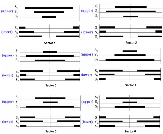
Space vector modulation is a method commonly used to control the three phase inverter bridge driving the motor. The method is based on dividing the [α, β] reference frame into six equal sectors, see Figure 4, and approximating the duty-cycle of three individual PWM signals. The appropriate sector, in which the reference vector lies, can either be derived from the [α, β] components directly or by first applying the inverse Clarke transform.
Depending on in which sector the [α, β] reference vector lies a specific PWM pattern is created, used to drive the MOSFET transistors in the inverter. By applying the correct PWM pattern, currents are forced to pass through the motor windings and a three phase AC can be shaped. Figure 5 show the switching patterns for each of the base vectors.
Space vector PWM provides good efficiency of the supply DC voltage compared to other modulation schemes, e.g. sinusoidal PWM. By viewing the three phase inverter as single unit instead of three separate transistor pairs, as in sinusoidal PWM, the voltage applied to the motor is increased form to [4].
13
14
3 SYSTEM HARDWARE
3.1 National Instruments single-board RIO-9632
The NI sbRIO-9632 embedded device is designed to be used for embedded control and data acquisition applications. It Features a 2M gates Field Programmable Gate Array (FPGA) from Xilinx and a 400 MHz real-time processor with 256 Mb non-volatile storage which makes the NI sbRIO-9632 board a powerful solution for applications where high performance and reliability are required [10]. There are 110 3,3V Digital I/Os, 32 16-bit analog inputs and four 16-bit analog outputs available on the device. The FPGA and the processor are synthesized and programmed respectively with NI LabView’s graphical programming tools. The host PC communicates with the board either through the built in 10/100BASE-T Ethernet port or through an RS-232 communication serial port. A short summary of specifications can be viewed in Table 1 below.
Table 1 Specifications of NI sbRIO-9632.
NI sbRIO-9632 Power requirements
Power Supply Voltage Range 19-30V Power consumption (no load) 7.75W
Network
Network Interface 10BASE-T and 100BASE-TX Ethernet
Compatibility IEEE 802.3
Communication rates 10Mb/s, 100Mb/s auto negotiated
Xilinx Spartan-3 Reconfigurable FPGA
Logic cells 46 080
Available embedded RAM 720 kb
Dedicated Multipliers 40
Freescale MPC5002B
Processor 760MIPS at 400MHz PCI communication with FPGA 32-bit PCI-Address/Databus
3.3V Digital I/O
Input/Output channel 110
Max. current per channel 3 mA 3.2 Adapter board
The Adapter board was designed to link all the essential parts of a motor controller system together. It was initially intended to be used together with the Xilinx Virtex 5 development board. A new version has been designed and extended with a connector to interface the NI sbRIO-9631/9632 board. The adapter board powers the Tamagawa resolver board, the inverter board and the motor as explained in section 3.2.1 and section 3.2.2.
3.2.1 Tamagawa Resolver board
The central unit of the resolver board is a coder device AU6802N1. The smart-coder converts the resolver signals which encode the mechanical rotational angle into a
15 12-bit digital signal. The output can be acquired either through a 12-bit parallel interface or a Serial Peripheral Interface (SPI) bus. There are several test points available on the card for troubleshooting purposes.
3.2.2 Inverter board
The inverter board comprises a full three-phase inverter bridge. Six Vishay Siliconix N-channeled MOSFETs are connected in a three armed bridge where each gate is driven by a high voltage three phase gate driver IC from International Rectifier. The gate driver has a built in protection against over-current and an over-temperature shutdown
functionality.
Two shunt resistors are connected in series with two outputs of the inverter bridge that connects to phase U and V of the motor. The phase currents are obtained through measurements of the voltage difference across the shunt resistors. These voltage differences are converted into two 12-bit digital signals through a two channel analog to digital converter (ADC). The currents passing through the phases are then calculated by Ohms law. The ADC data can only be acquired from the built in SPI communication bus. The board can be viewed in Figure 6.
16
4 IMPLEMENTATION
During the developing process two separate systems were created. First the single axis system described in [1] and [2] was reassembled and thoroughly tested in a laboratory test bench, see section 7.2. Second, a multi axis system capable of controlling two motors individually was developed, see section 4.3.
The test results from the test bench were compared with the results from a MATLAB/Simulink model of the system to verify the functionality and served as a benchmark test when evaluating the multi axis system. For a successful result the performance of the controller shall notot decrease when adding multiple axes. Both systems were designed using components developed in [1] and [2]. However, all components were tested and verified at implementation and some were modified to provide proper functionality. This section describes the implementation of the complete system on the FPGA. In section 4.1 the system design and implementation of the
components are provided. Section 4.2 and section 4.3 provides a description of how the components are implemented in the single axis system and in the multi axis system.
4.1 System design
Both systems, i.e. the single axis system and the multi axis system, are designed using the components described in section 4.1.1 to section 4.1.7. The systems are designed as several loops executing in parallel. The communication between the loops is handled by dedicated memory areas in the block RAM memory, see Figure 7. For a rapid
prototyping application it’s important for the user to be able to interact with the
controller. Therefore, a user data memory area is added where user data such as PI and feed forward controller parameters are stored. It also holds the data that is of interest for monitoring, e.g. Id, Iq values and speed. The user data is stored in controls and indicators, displayed on the front panel for easy access.
Figure 7 System design
All calculations in the systems are performed using fixed point arithmetic. The fixed point data type is configurable to provide the accuracy needed to represent the data, i.e.
FOC loop
User data memory area
Output Memory- area Motor interfaces Input Memory- area
17 the total number of data bits and number of integer bits can be modified. The fixed point representation for each of the variables can be found in Table 26 in appendix C.
4.1.1 The Clarke transform
The Clarke transform is implemented straightforwardly using LabView blocks. Figure 8 shows the realization of equation (1) and (2) where A and B are the measured phase currents in winding U and V. The transform used is magnitude invariant, i.e. the currents maintain their amplitude after the projection onto the two dimensional [α β] plane.
Figure 8 Clarke transform implemented in LabView
4.1.2 The Park transform
The Park transform is as the Clarke transform easily implemented. By using the Iα and Iβ derived in the Clarke transformation and the sine and cosine components of the motors electrical angle, Id and Iq are derived. The block component shown in Figure 9
corresponds to equation (3) and (4).
Figure 9 Park transform implemented in LabView
4.1.3 Controllers
To control the Id and Iq components two types of controllers are used, PI and a feed forward control. The feed forward controller is used to reduce the load on the PI regulators when the motor is running in steady state while the PI regulators are
18 designed to regulate the error produced by the feed forward controller and handle
transients associated with sudden increases in speed or load. To obtain this functionality the feed forward controller and the PI controllers operate in parallel.
4.1.3.1 PI controllers
The PI controllers used are the built-in PID blocks described in section 4.3.1.4. Two PI regulators are implemented to regulate the Id and Iq values derived in the Park
transform. The outputs from the regulators are calculated as a sum of equation (10) to (12). However, for this application no derivative term is used so the output is equal to the sum of up(k) and ui(k).
(10)
(11)
(12)
Where
e(k) = set point(k) – PV(k)
PV(k) = value of process variable on the k:th call after initialization
4.1.3.2 Feed forward control
Feed forward control is an open loop type of control, i.e. no feedback from the system controlled is used. The feed forward algorithm represents a model of the electrical dynamics in the motor, defined by the equation (13) and (14) [1]:
(13) (14) Where
Rs = line to line resistance in the motor
Ld = Lq = line to line inductance in the motor
i*sd = motor flux reference value
i*sq = motor torque reference value
ωs = electrical speed of the motor in rad/s
λ = magnetic flux linkage of the motor
For this application no field weakening is required, i.e. the motor flux reference value will always be set to zero. Hence, all terms holding the i*sd value can be removed from the equations resulting in equation (15) and (16).
(15)
19
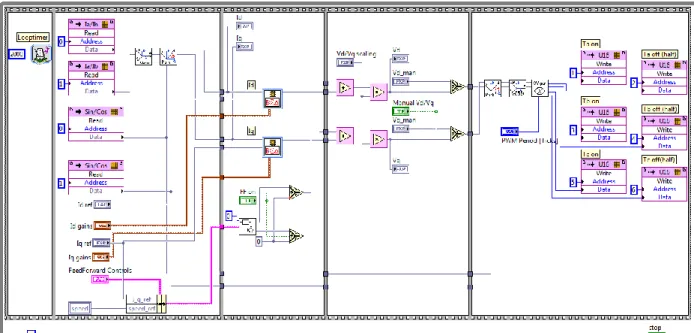
Figure 10 Implementation of equation (19) and (20)
In Figure 10 the implementation of equation (15) and (16) is shown. The data to be processed is read from the feed forward controls, see Figure 11, and passed into the algorithm. Along with the data read from the controls the i*sq value from the previous iteration of the loop is read from a block memory for the derivative term. To synchronize the signals being passed into the algorithm a sequence is used.
Figure 11 Feed forward controls
4.1.3.2.1 Derivative term of Uq
One problematic part of the feed forward algorithm is the derivative term
. When
using the algorithm in a multichannel application, i.e. when the controller is used to control multiple entities, the previous value of i*sq must be stored in a safe way. To achieve safe storage a case structure along with a block RAM memory is utilized. For each case the previous value of i*sq is fetched from a predefined address in the memory, selected by the Channel index where the channel index corresponds to an individual motor. When the previous i*sq value has been collected the current i*sq value is written to the same memory address.
20 To calculate the derivative of i*sq the previous value is subtracted from the current value. The result is multiplied by
, i.e. the sampling frequency of the control loop in Hz,
resulting in the value corresponding to
.
This solution introduces a problem if the difference between the old i*sq and the current
i*sq is large. If the difference is large, the derivative will be large and might cause numerical problems in the fixed point representation. However, when viewing the feed forward controller as a part of a complete system, it will be used together with a speed controller and a path planner. The outer control loops will gradually increase or
decrease i*sq according to a torque profile, i.e. no large leaps in the i*sq value, If the reference value increases gradually the derivative term will not cause any problems. To prevent problems when testing the system without the outer loops a saturation function was added that holds output from the derivative term in the interval -16 to 15,99. Thus, no overflow can be expected in the integer part of fixed point representation while maintaining good resolution in the decimal part when adding the derivative term to the
Rs*i*sq term.
4.1.3.2.2 Deriving the Feed Forward parameters
Depending on what motor is to be controlled, different parameters must be applied to the feed forward algorithm. The data to be used when deriving the parameters are found in the data sheet of the specific motor. For the Rs and Lq parameters the line to
line values should be used and can be derived by using equation (17) and (18).
(17)
(18)
The formula for deriving lambda is shown in equation (19). Note that the rated current must be represented in its peak value. The algorithm shown in Figure 10 requires that the data in speed_ref represents the electrical angular velocity. However, if only the mechanical angular velocity is available it can be converted to the electrical angular velocity by applying equation (20). Moreover, the algorithm also requires that the data in Iq_ref , i.e. i*sq, is represented in peak value.
(19)
(20)
Where np = number of pole pairs in the motor
4.1.4 The inverse Park transform
To rotate the regulated voltages derived from the regulators back to the static [α β] reference frame the inverse Park transform is used. The transform uses the Vd and Vq
21 values provided by the regulators along with the same sine and cosine values as the Park transformation to perform the operations corresponding to equations (5) and (6). Figure 12 shows the implementation of the equations.
Figure 12 Inverse Park transform implemented in LabView
4.1.5 The inverse Clarke transform
For this project a modified version of the Clarke transform is used. Compared to equations (7) to (9), Vα and Vβ component are inverted, thus resulting in a 90° counter clockwise rotation of the reference vector. By using the modified inverse Clarke
transform, the SV- modulation generation becomes more straightforward and requires fewer calculations [11]. Equations (21) to (23) show the modified inverse Clarke and Figure 13 shows the implementation of the equations. Similar to the Clarke transform, the version used is magnitude invariant.
(21)
(22)
(23)
22
4.1.6 Space vector modulation generator
The space vector modulation generator uses the output from the inverse Clarke transformation to determine in which sector the voltage vector lies. To determine the sector the value of va, vb and vc, denoted Vr1, Vr2 and Vr3 in Figure 14, are used. If the
value is greater than zero the respective bit is set to one in a three bit number. The number is then used to select in which sector the vector lies according to Figure 4.
Figure 14 Space vector modulation generator
Depending on the sector the PWM on-times T1 and T2 is extracted from X,Y,Z, calculated according to equation (24) to (26).
(24)
(25)
(26)
When the on-times have been extracted T1 and T2 are scaled to a corresponding ratio of the PWM period and the individual on-times for three phases are derived as a
combination of T1 and T2, see equation (27) to (29).
(27) (28) (29)
After deriving the individual on-times for the phases the values are applied to the correct phase, depending on in which sector the vector lies [11]. In the final stage the on-times are converted into a center aligned PWM by subtracting each on time from the PWM period and the off-time for each phase is derived by dividing the on-time in two.
The final stage is used to adapt the algorithm to the FPGA. The algorithm used, described in [11], is adapted to be used in a DSP where the calculated on-times are
23 compared to an internal PWM counter. When the counter reaches the value of Ta, Tb
and Tc the output from each PWM generator is inverted meaning that what actually is
being calculated is the off-time, see Figure 15. However, in the FPGA no PWM counter is used so the on and off times for the PWM signal must be inverted.
Figure 15 PWM generation in a DSP
To verify the functionality of the space vector modulation generator it was used together with the inverse Clarke. By monitoring the output from the generator when manually entering the [α β] coordinates for each of the base vectors, see Figure 4, the PWM patterns can be created. To provide the proper PWM patterns according to [4], the output for the six sectors should correspond to Figure 16.
24
4.1.7 Motor interfaces
To interface the motors to the FPGA a set of VI:s is required. The VI:s are used to either actuate the motors or read sensor data from the motors.
4.1.7.1 Reading ADC:s measuring motor currents
To obtain data from the ADC:s measuring the motor currents in the inverter board the current measuring scheme described in [1] is used. The current data in winding U and V are read from the ADC:s via a SPI bus and is represented as a 12 bit number. When all data is read from the ADC:s the number is scaled to represent a current between -8 to 8 amperes and stored in block RAM memory, see Figure 17.
Figure 17 ADC interface with current scaling
4.1.7.2 Motor position data from a resolver
For position feedback a resolver is used along with the motor. The resolver provides two analog voltages representing the sine and cosine of the motors mechanical angle. To interpret the signals the AU6802 Smartcoder from Tamagawa Seiki Co. is used. The smartcoder provides the excitation signal for the resolver and converts the resolver output to a 12 bit number, representing the mechanical angle. In order for the FOC algorithm to function properly it is important to obtain correct data about the motors position. If erroneous data is received it will cause the system to derive a faulty electrical angle and hence deploying a faulty pattern from the SV-PWM generator. The 12 bit number is read from the smartcoder via an SPI interface and is converted into sine and cosine of the electrical angle, see Figure 18. The number is also converted back into the motors mechanical angle for monitoring and stored in a FIFO to be used in speed
calculation, see section 4.1.7.2.1. When the number has been converted it is stored in the block RAM memory as well as displayed in indicators.
25
Figure 18 Interface to the Tamagawa smartcoder
4.1.7.2.1 Speed calculation from resolver data
The electrical angular velocity of the motor is calculated by adding ten consecutive resolver readings stored in a FIFO and calculating the average speed over those readings. The result is presented in radians per second, see equation (30).
(30)
Where
Tsr= resolver sampling period
np = polepairs of the motor
pos = motor position from resolver
To correct the error induced when the resolver passes the zero position the method described in [1] is used. The difference between the current resolver value and the last resolver value is compared to two constants that represent the largest difference that can occur in either direction of rotation, see equation (31). However, in this
implementation the constants are larger than required to support slower sampling rates of the resolver. If the difference is larger or smaller than the constants one revolution, i.e. 4095, is subtracted or added to the result, see Figure 19.
26
Figure 19 Speed calculation loop
4.1.7.3 PWM generation
To generate the PWM signals for the inverter bridge, three parallel sequence structures are used. The PWM signals are created by assigning the output pins a boolean true or false value followed by a wait time derived in the SV- modulation generator, see section 4.1.6. After the wait time a new value is assigned to the output followed by a wait, thus creating the PWM patterns. The PWM generator also generates the synchronization signal for current measurements.
The value of the PWM signals for the upper and lower transistor in each transistor pair is always assigned the opposite value of each other to avoid that both transistors are open simultaneously, creating a short circuit in the inverter bridge, see Figure 20.
However, the transistors do not open and close instantly at a change in the PWM signal, i.e. rise time and fall time, which might cause a short shoot through at each switching.
27 Dead time is introduced in the PWM signals to avoid shoot through where booth signals are set to low for a short period, allowing the transistor in open state to close before the transistor in closed state opens, see Figure 21. In this implementation the dead time (td) cannot be greater than a few percent of the PWM period or it will affect the frequency of the PWM too much, reducing the performance of the controller. However, if the dead time is compensated for in the SV- modulation generator it can be increased.
Figure 21 PWM signals for one transistor pair with (right) and without (left) dead time
The driver circuit on the inverter board uses inverted logic to drive the signals for the transistor gates. Therefore, the output from the PWM generator must be inverted in order to provide the correct PWM signals for the transistors
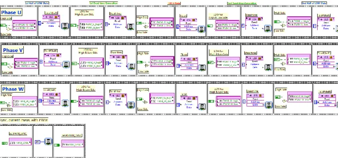
4.2 Single axis system
The single axis system is implemented as a main loop where the components Clarke, Park, regulators, inverse Park, inverse Clarke and SV- modulation generator are
included as sub VI:s. In each sub VI the controls and indicators are connected to the VIs connector pane, creating input and output ports to VI.
28 The system shown in Figure 22 is a revised version of the system developed in [1] and [2]. However, a few changes have been introduced to the system.
Block RAM memories are used to hold the data passing in and out of the loop A sequence structure has been added to synchronize signals
The fixed point representation has been revised to assure no overflow when reaching high currents
A revised version of the feed forward controller has been added, see section 4.1.3.2
The sequence used to synchronize the signals is divided in five frames. In the first frame the period of the loop (Ts) is set where the period is defined in system ticks and can be calculated according to equation (32).
(32)
In the second frame all data to be used in the calculations are read from the input block RAM memories and the front panel, i.e. current data, resolver data and user data. The Clarke and Park transformations are also performed. In the following frames the data is subsequently regulated and further processed by the regulators, inverse Parke, inverse Clarke and SV- modulation generator before it is finally written to the output block RAM memory. Note that in the fourth frame the Vd and Vq components are multiplied by a scaling factor to normalize the vector to the DC supply voltage for the inverter. For further details, see section 4.4.
To interface the inverter bridge and the sensors to the FPGA the components described in section 4.1.7 are included in three parallel loops as sub VIs, see Figure 23. A
separate loop is implemented to turn the inverter on and off and change the dead time at runtime.
Figure 23 Motor interfaces running in parallel to the FOC loop
To monitor data and manipulate parameters, indicators and controls are placed at the front panel, see Figure 24.
29
Figure 24 Front panel for the single axis system
In a rapid prototyping application it is desirable to be able to look at the data present in the controller graphically. The FPGA module in LabView does not provide the possibility to graphically present data. Therefore, the data must be transferred to another
processor to be displayed in a graph. In this application the data is transferred to the PPC where the data can be presented in graphs using DMA FIFOs, see Figure 25. The sbRIO board holds three onboard DMA-channels which limit the number of DMA FIFOs to no more than three. However, one FIFO can be used to transfer multiple types of data. This method requires that the developer keeps track of the order in which the data is written to the FIFO or the data will be scrambled when presented.
30
Figure 25 Loop for writing data to the FIFOs
4.3 Multi axis system
When controlling multiple motors with the FOC algorithm, the same calculations are performed for all motors but with different data. If a method can be developed where one FOC loop can perform the calculations for all motors it would greatly reduce the number of required resources for a multi axis control system. However, during the development of the multi axis system several approaches were considered.
Developing a system where the calculations are distributed between the FPGA and the PPC.
Developing a system with one FOC loop for each axis
Developing a system where one FOC loop on the FPGA performs the calculations for all axes sequentially
Developing a system where one FOC loop on the FPGA performs the calculations for all axes but for multiple axes simultaneously.
In order to determine which method to use, a series of tests were performed on the sbRIO platform, see section 4.3.1. The aim of these tests was to investigate and evaluate the possibilities and limitations of the platform when developing a multi axis control system using LabView.
The results from the initial tests showed that the first two options above would not be possible due to low performance in the PPC and timing problems on the FPGA. Therefore, an attempt was made to develop a system where the calculations were performed for all motors simultaneously but at different levels of the loop using shift registers, see Figure 26. However, the method proved to suffer from synchronization problems and a fast growing complexity so the option was abandoned. Instead a solution where all calculations were performed by one single FOC loop in serial was chosen.
31
Figure 26 Multichannel FOC loop with shift registers
The control loop was designed in a similar way as the loop in the single axis system, see section 4.2, with the difference that the data to be processed had to be collected from different memory addresses. To solve the problem with reading data from different addresses a simple case structure and counters were used. Each iteration of the loop the counter changed the value used to select case, see Figure 27. This method is used in all loops where data for multiple axes is being processed. When testing the system only two motors were used so only two cases were needed. To facilitate the case selection a boolean counter was used that was negated each iteration of the loop. However, when adding more motors to the system the counter should be changed to a numerical counter and more cases can then be added.
32 The design of the multi axis system follows the same design principle as the single axis system with several loops executing in parallel. To save resources on the FPGA the scaling of resolver data and current data has been moved from the separate VIs to two scaling loops, as can be seen in Figure 28.
Figure 28 Overview of the multi axis system
The scaling loops are implemented to continuously execute the scaling algorithm on the data most recently read form the sensors, see Figure 29 and Figure 30. The loop period has been set short to minimize the delay time induced when processing the data in an additional loop and can be calculated according to equation (32).
Figure 29 Current scaling loop
FOC loop
Input memory area Output memory area Motor interfacesMotor one block Motor two block
User data Scaling loops Sensor memory area
33
Figure 30 Resolver scaling loop
In Figure 31 the final multi axis FOC loop is shown. The design is much similar to the single axis system with the addition of case structures and counter. Using this design, the FOC loop, see Figure 28, operates as a processing unit where data is shifted in and out of the loop which only requires that one set of resources is allocated at compilation. However, it also requires that the loop must be executed at the sampling rate for each individual motor times the number of motors in the system, i.e. more motors mean lower sampling rate for each individual motor. In section 7.3 an analysis of the execution time of the loop is provided to show the minimum loop period possible.
34
4.3.1 Initial tests
This section of the report provides a description of the tests performed on system features considered key features when choosing a method for the final solution. To determine which approach to use a series of tests were performed. In section 4.3.1.1 the performance of the DMA communication between the FPGA and the PPC is evaluated and in section 4.3.1.2 an estimation of the PPC performance in provided. Section 4.3.1.3 provides an overview of how the utilization of FPGA resources is affected when more dedicated multiplicators than available are required and finally in section 4.3.1.4 the functionality of the built-in multichannel PID blocks is verified.
4.3.1.1 DMA communication performance
To evaluate the performance of the built-in DMA functions in LabView a test program was designed to measure the time consumed when sending data from the FPGA to the processor and back. The LabView FPGA-module contains built-in functions for
designing FIFO-blocks, intended for DMA communication between the FPGA and a remote host computer. The FIFO-blocks are implemented in logic on the FPGA and can be accessed remotely via an onboard PCI-bus.
When using DMA communication, each FIFO block has a dedicated direction of data transfer; either from the FPGA to the host (in this case the PPC) or from the host to the FPGA. Hence, two FIFO blocks had to be implemented for two way communication. Using this setup, one onboard DMA channel will be used for transferring data from the FPGA and one channel will be used for transferring data to the FPGA. The size of the FIFO and the data type of the elements stored in the FIFO is static and specified at implementation. The elements size was chosen with respect to internal architecture of the processor, i.e. 32 bit [3].
4.3.1.1.1 Program design for testing the DMA performance
The FPGA VI was designed as a while loop running continuously with a period of one second. Inside the while loop a sequence of operations is performed, see Figure 32. In the first step of the sequence the number of system ticks since startup is recorded followed by a write operation to the FIFO block. The FIFO write operation has a zero tick time-out variable, meaning it times out instantly if there is no space available to write in the FIFO.
35 When reading from the FIFO the operation has a time-out variable of -1, representing no time-out and the program waits until there is something to read from the FIFO. Finally, the system clock ticks are recorded again and the number of ticks spent in the loop is derived by subtracting the first reading from the second reading. This method induces a small error in the result due to the fact that it takes a few ticks to move between the frames in the sequence. However, compared to the total time spent in the loop this error can be ignored. When testing the performance of sending more than one element, two for-loops were added around the write and read operations, where one element is written or read each iteration of the loop. The performance was tested for 10, 50 and 100 iterations. One additional test was also made to estimate the time it takes for the FPGA to write one element to the FIFO, this test was performed using the same method as described above.
To assure that the loop is completed, the value of the element was set from a control in the front panel. When an element is read from the FIFO it is displayed in an indicator on the front panel along with the number of ticks spent in the loop.
The VI running on the PPC is designed to read a specified number of elements from “input” FIFO and return them instantly to the “output” FIFO, see Figure 33. The Read operation waits until it can read the pre-specified number of elements and writes them to the “output” FIFO as an array of elements. When testing the performance of multiple elements, the Number of elements variable was adjusted to the same value as the loop count on the FPGA.
Figure 33 PPC VI for testing the DMA performance
4.3.1.1.2 Results from DMA tests
Figure 34 show the results obtained when sending elements from the FPGA to the PPC and back. For each test ten values were recorded and an average was calculated. The data type of the elements used is Unsigned 32.
The results indicate that the LabView environment introduces lots of overhead on the PPC. By viewing the graph in Figure 34 one can see that the time it takes to send data from the FPGA to the PPC and back is linear to the number of elements sent. By studying the equation for the trend line it can be concluded that the transmission time
36 for sending one element is approximately 0,7 µs and the overhead on the PPC is
approximately 120 µs. The overhead in the system corresponds to the time it takes to transfer the data from the built in DMA controller in the PPC to the program.
Table 2 Time to write one element to the FIFO
On FPGA Time
Write one element to FIFO >1 µs
Figure 34 Results from DMA performance tests
The results shown in Figure 34 can be used to estimate the bandwidth of the DMA communication. By using the time it takes to transfer one element to the PPC and back to the FPGA the bandwidth can be calculated according to equation (33).
(33)
The size of the element must be multiplied by two since the time is measured for two way communication. To represent the bandwidth in bytes per second the element size is divided by eight. Nr of elements 1 10 50 100 4830 5115 6036 7350 1 Tick = 0,000000025 4819 5045 6021 7571 4642 5160 6015 7300 4813 5018 6096 7381 4756 5117 5973 7545 4729 5002 6046 7476 4811 5093 6122 7452 4702 5120 5987 7430 4727 5175 5993 7261 4800 5087 6000 7331 Ticks average 4762,9 5093,2 6028,9 7409,7 Time average 0,000119073 0,00012733 0,000150723 0,000185243 s FPGA system ticks y = 7E-07x + 0,0001 0 0,00002 0,00004 0,00006 0,00008 0,0001 0,00012 0,00014 0,00016 0,00018 0,0002 0 20 40 60 80 100 A ve ra ge t im e ( s) Number of elements Series1 Linear (Series1)
37 When entering the values seen in the column for one element in Figure 34 in equation (33) the result is:
When calculating the bandwidth according to equation (33) the overhead on the PPC is included in the calculations. However, to calculate the bandwidth of the PCI bus alone the overhead can be subtracted from the transfer time. Assuming that the overhead is constant for any number of elements the bandwidth can be calculated according to equation (34).
(34)
When entering the values for transferring one element in equation (34) the result is:
As can be seen in the results from the calculations above the speed of the PCI bus is sufficient for transferring large amounts of data. However, the overhead induced by LabView on the PPC reduces the speed too much to use the PPC for any high speed calculations.
4.3.1.2 Performance of PPC real-time processor
In an attempt to estimate the utilization of the CPU when running a relatively simple program, the existing feed forward controller was converted to run on the PPC instead of the FPGA. The program was implemented as a Real-Time task with the LabView RT-module library. To implement Real-Time systems LabView RT-RT-module uses the
VxWorks RTOS as a platform where developers can implement the tasks [9]. The tasks are implemented as timed loops where the loops can be assigned the appropriate attributes such as period, priority and deadline.
To minimize communication overhead no front panel communication was used. A host VI was developed to run on the PC where all controls and indicators were placed. The communication between the PC and the PPC is handled by network-published shared variables, shared via the Ethernet connection between the sbRIO-board and the PC. The variables were configured in such a way that they do not affect the real-time properties of the task.
4.3.1.2.1 Feed Forward Controller running on the PPC
The feed forward controller was converted to operate on the PPC. In the existing version of the controller all calculations were performed by using fixed-point arithmetic,
38 the PPC on the other hand uses double precision floating-point arithmetic [3]. Hence, all variables and operators were changed to support the double data type.
To measure only the time consumed when performing the calculations a sequence was added around the operators. Time was measured in the same way as described in 2.1., with the difference that time is displayed in µs instead of ticks. Since the objective of this test did not include communication with the host PC, all operations on the shared
variables was handled outside the sequence, see Figure 35. Tests were also performed with the communication included in the measurements but the results were very
unstable. For comparison the original code was run and measured on the FPGA. The period of the timed loop was set to one second in order to be able to view the result of the measurement.
Figure 35 PPC VI for testing the feed forward Controller
For communicating with the PPC a VI was developed to run on the host PC. From the host VI all shared variables can be manipulated. The loop is set to run at the same periodicity as the PPC VI but without any real-time properties.
4.3.1.2.2 PPC performance results
Table 3 shows the results from timing calculations when running the feed forward controller on the PPC.
Table 3 Execution time for feed forward controller running on the PPC
Ticks Time (µs)
Only calculations 83-84
Calculations and communication ~250±100
39 In Table 3 it is shown that it is not possible to run tasks such as the feed forward
controller fast enough on the PPC. Just considering the calculation time it would take 249-252 µs to perform the calculations for three motors, translating into a frequency of approximately 4 kHz. Adding the communication with the FPGA would reduce that frequency even more.
4.3.1.3 FPGA utilization when using numerous multiplications
One of the biggest issues of the existing single axis system is the use of dedicated multipliers on the FPGA [1]. The FPGA holds a number of dedicated multipliers (in this case 40 [13]) that can be used for arithmetic operations, placed as seen in Figure 36. When all dedicated multipliers have been used, additional multipliers are created from logic during the synthesis process if needed. Therefore, a test was performed to evaluate how multiplications affect the utilization of the FPGA.
Figure 36 Architecture of the FPGA
To perform the test the feed forward controller developed in [1] was used without any modifications, see Figure 37. The feed forward controller comprises a large number of multiplications which makes it suitable for this test. Blocks such as controls and
indicators will also contribute to the use of system resources. However, the uses of those resources are assumed to be linear to the number of blocks.
When testing for FPGA utilization the code was synthesized and the system utilization was extracted from the Xilinx compilation log. For each synthesis one extra instance of the controller was added in the interval from one instance of the controller up to seven instances, providing a range from 12 multiplications to 84 multiplications in steps of 12. All controllers are designed to run in parallel which guarantees that one resource cannot be used by more than one controller.
40
Figure 37 feed forward controller VI for FPGA
4.3.1.3.1 FPGA utilization results
Figure 38 shows the results on how the system resources are utilized when using numerous multiplications in the algorithm. The top graph shows the number of resources used and the bottom graph shows explicitly the number of multiplicators used, both compared to the number of multiplications present in the system.
When studying the lower graph in Figure 38 it is interesting to see that not all dedicated multipliers are used when 72 and 84 multiplications are used in the system. This can be explained by studying Figure 36, all the multipliers are placed at the periphery of the FPGA. When routing the signals onto the device during the synthesis process it is not possible for the synthesizer to meet all timing constraints by including all multipliers in the circuit. Each bit of the variables used for the calculations translates into a signal on the FPGA that requires a wire on the device. The conclusion from this result is that the biggest problem is not the use of dedicated multiplicators in the code but fulfilling all timing constraints at synthesis. Therefore, all variables in the system should be reduced to the smallest size possible and still be able to carry a sufficient amount of data.
41
Nr of multiplications 12 24 36 48 60 72 84
Slice Flip Flops 1192 1958 2723 3488 4401 5364 6185
4 input LUTs 849 1241 1647 4257 8084 13037 17156 MULT18x18 12 24 36 40 40 36 35 Slices 960 1490 2441 3899 5952 8921 10938 0 1000 2000 3000 4000 5000 6000 7000 8000 9000 10000 11000 12000 13000 14000 15000 16000 17000 18000 19000 0 5 10 15 20 25 30 35 40 45 50 55 60 65 70 75 80 85 90 U se d r es ou rc es Number of multiplications 4 input LUTs Slice Flip Flops Slices 0 5 10 15 20 25 30 35 40 45 0 5 10 15 20 25 30 35 40 45 50 55 60 65 70 75 80 85 90 U se d m ul ti pl ic at or s Number of multiplications MULT18x18
Figure 38 System utilization when using numerous multiplications
4.3.1.4 PID tests
To implement a shared FOC loop it is essential that the calculations in the loop are performed without any interference from previous iterations of the loop. One part of the algorithm where this could be a problem is the integral part of built-in PID regulator in LabView. The built-in PID block in LabView provides the possibility to configure it to operate as a multichannel regulator where multiple entities can be controlled. Since the integral part stores the error data from previous iterations it must be verified that the data from all entities is stored and manipulated independent of each other.
42 To verify the functionality of the PID blocks a simple test program was designed, see Figure 39. The program is designed to use the PID block as a dual-channel PI controller where the only difference between the channels is the integration factor, Ki.
Figure 39 Implementation of PID test program
For both channels the proportional factor Kp is set to one, the derivative factor Kd is set to zero, the process variable is kept constant at zero and the set points for both
channels are set to one. For simplicity the loop period is set to 1000 ms. Using this setup the expected result is that the output will start at one, corresponding to the Kp value, then continue increasing each iteration of the loop with a slope corresponding to
Ki. For channel zero the Ki value is set to 0,25 and for channel one the Ki value is set to 0,5. These parameters were chosen so that the result could be easily verified. With a loop period of one second the output is expected to increase one every four seconds for channel zero and one every two seconds for channel one. The expected outputs are derived by solving equation (35).
(35)
In Figure 40 the output from both channels are graphically represented. The left graph shows the output from channel zero and the right graph shows the output from channel one. As can be seen in both graphs, the output rapidly increases to one in the beginning of the graphs. After the first step the output increases at individual rates just as
expected, for channel zero the output reaches two in four steps and for channel one the output reaches two in two steps. Hence, it can be derived that the calculations are performed individually without interference from one another.
43
Figure 40 Output from the multichannel PID (Note that the time scale does not correspond to seconds)
4.3.1.4.1 Initial PID settings
The built-in PID block in LabView has a number of parameters that can be modified for the PID to provide proper functionality. When incorporating the PID block in the
program, all initial settings are done using the configuration panel, see Figure 41.
Figure 41 Configuration panel for the PID block
Number of channels:
Specifies how many channels will be realized during compilation. Initial set point:
Specifies the set point of the regulator the first time the regulator is executed. Sampling time:
Specifies the sampling time of the regulator in seconds. Must be set to the same value as the period of the loop the regulator operates in. If the regulator is set to
44 operate in more than one channel, the regulator will sample one channel each iteration of the loop.
High and Low limit:
Specifies the high and low saturation levels of the regulator. The values are initially applied to all channels.
Initial Gains:
Specifies the initial gains for all channels. The integral time and derivative time must be specified in minutes. The quantized initial gains are calculated and displayed on the panel according to equation (36) to (38).
(36)
(37)
(38)
Where Ts is the Sampling time Ts (s) at which the control loop runs.
4.3.1.4.2 Runtime PID settings
The PID block in LabView provides the possibility to change some parameters at
runtime. When using the PID block as a single channel regulator the PID gains, the high and low saturation levels and the set point can be changed. For a multichannel PID the same parameters as for the single channel PID can be manipulated and it also provides the possibility to address which channel the parameters should be applied to, thus providing the possibility to have individual settings for all channels. Figure 42 shows the controls for a single channel PID and in Figure 43 the controls for a multichannel PID is shown.
Figure 42 Single channel controls Figure 43 Multichannel controls
45
4.4 Vd/Vq scaling
The output from the regulators represents the Vd and Vq components corresponding the to the voltage applied to the motor. In order for the SV- modulation generator to function properly, the magnitude of [Vα Vβ] cannot be greater than the radius of the circle fitted inside SV- modulation hexagon, see Figure 44. When applying maximum voltage to the motor the magnitude of [Vα Vβ] is equal to the circle radius. If the magnitude is greater than the radius of the circle the duty cycle of one or several of the output PWM signals may be greater than the PWM period or negative.
Figure 44 Maximum magnitude of the [Vα Vβ] vector
In a SV- modulation application the circle has a radius of [4]. In order to fit the vector inside the circle, the vector must be normalized. This is done by scaling the Vd and Vq components by a factor that normalizes them to the DC supply voltage, see equation (39).
(39)
In these applications the scaling is performed before the inverse Park transformation. The inverse Park transformation is just a rotation which means that the magnitude of the vector will remain. The scaling could just as well be performed after the inverse Park transformation.
46
5 SIMULATION
5.1 MATLAB/SimulinkThe aim of modeling the system in Simulink is to be able to verify some of the results from the mechatronic test bench that will be used to test the implemented system later. It is both difficult and time demanding to derive a complete model of the system since the system stretches over three different physical domains (electric, magnetic and the mechanic). It also requires a very good understanding of the motor and well defined model parameters. Therefore, a simplified and reduced model of the FOC-algorithm will be modeled and used to control and run a built in PMSM block provided by the toolbox SimPowerSystem. SimPowerSystems is a frequently used toolbox in Simulink for simulations of electronic and power electronic systems.
Normally, a simulation model of the system is created prior to the implementation of it. This case is an exception since it is a part of a rapid prototyping project where the modeling and implementation are carried out in parallel. The model is therefore based on the implementation instead of the other way around.
5.2 MOTOR MODEL
The electrical dynamic motor equations for the PMSM block in SimPowerSystem in the dq- reference frame can be expressed as:
(40) (41)
Where: Vd is the voltage flux component, Vq is the voltage torque component, R is the armature
resistance, Ld is the inductance flux component, Lq is the inductance torque component, ω(t) is
the rotor electrical speed in rad/s and λ is the flux linkage.
The inductances for the dq-frame were calculated with equation (42).
(42)
And the mechanical dynamics are as follows:
(43)
(44)
Where: J is the rotor moment of inertia, TM is the mechanical torque, TE is the electrical torque,
47 Equations (38) to (42) are the general motor dynamic equations for a PMSM in the dq-reference frame.
A complete list of all motor parameters used in the simulation can be viewed in Table 4. All values except for B are based on data from the datasheet of M103. B is the
combined viscous friction of the rotor and the load. It has not been determined for the M103 and is therefore set to 0,001. This value is only an arbitrary value based on values used in other simulations. B has to be determined later to get the proper
mechanical properties of the motor. The emphasis of the simulations will not be on the mechanical parts but on the electrical and the control parts of the system until then.
Table 4 List of simulation parameters
Rs 1.8 Ohm Ld 0,53mH Lq 0,53mH Lambda 0,005 J 0,0011*10-4 B 0,001
5.2.1 The reduced FOC-Algorithm controller with power electronics
Figure 45 shows an overview of the simplified controller implemented in Simulink and SimPowerSystems.
The PMSM block (labeled M103) has four different inputs and the user can choose from up to 13 different outputs to monitor. The first input (labeled w in the figure) specifies if the motor should run at a certain speed w rad/s or be loaded with a specific torque Tm. The three remaining inputs are the motor windings A, B and C where the three phase inverter outputs are connected to.
The 13 outputs are optional and can be selected through a bus. The outputs are the stator currents A, B and C, Id/Iq, Vd/Vq, the rotor speed (rad/s), the rotor angle (rad/s), the Hall Effect signals A, B and C and the electromagnetic torque (Nm).
The user can also specify the type of back emf waveform the motor has. It could be of either a sinusoidal or a trapezoidal waveform type for a PMSM. Moreover, the standard motor parameters such as the stator resistance (Rs), inductances in the dq frame (Ld
Lq), λ0, torque and voltage constants (Kt and Ke), and the number of pole pairs (np) needs to be specified. There are also sets of predefined motor parameters and characteristics to select from.
The PI controllers use the same parameters as the implemented system, i.e. the proportional gain Kc = 1 and the integral gain Ki = 0,01. The sample frequencies of the regulators are set to 20 kHz each.
48 The PMSM block generates the currents in terms of Id and Iq, thus there is no need to use the Clarke and Park transform to convert the three phase currents into the dq- reference frame. The feedback currents will be directly acquired from the motor outputs. The rotor position is also generated by the motor block directly. Thus, there is no need to model a position encoder.
Figure 45 FOC-Algorithm in Simulink/SimPowerSystems
Figure 46 shows the subsystem called Three-Phase Inverter in Figure 45 which
includes the SVPWM block and the three phase inverting bridge. The SVPWM block is also provided from SimPowerSystems and differs a bit from the one that is implemented on the FPGA in the sense of how the reference vectors are calculated and also how the modulation index is defined. Nevertheless, the basic principles are the same. Another difference is that the block uses the alpha and beta components directly as inputs instead of the Id/Iq components generated by the inverse Clarke transform. Thus, the model will not include the inverse Clarke transform in the simulations. The inverse Park transform is however needed to transform the variables back from the rotating frame into the stationary frame and can be seen in Figure 47.
The three phase inverter bridge uses six ideal MOSFETs with internal diodes in parallel with a snubber resistance in series. The pulses labeled [t1] to [t6] are connected to the gates on the MOSFETs. The three phase output connects to the PMSM block. The DC Voltage Source is set to 24V.
49
Figure 46 SVPWM Generator and three phase inverter subsystem block
Figure 47 Inverse Park transformation block
5.2.2 Feed Forward Controller
The feed forward controller is based on the equations from section 4.1.3.2 and is just a simple model to simulate the outcome in terms of Vd and Vq for different sets of Iq_refs
50 for the same inputs. The subsystem and the block diagram of the block can be seen in Figure 48 and Figure 49 respectively.
The derivative term of Iq_ref has been left out since it will not have any effect on the
output if the reference value is kept constant. The scaling term is the same as in the implementation, i.e.
.
Figure 48 Feed forward controller internally
Figure 49 Feed forward controller
When simulating the feed forward controller the same motor parameters as the M103 motor in section5.2 are used.