http://www.diva-portal.org
Postprint
This is the accepted version of a paper published in Transactions of the Institute of Metal
Finishing. This paper has been peer-reviewed but does not include the final publisher
proof-corrections or journal pagination.
Citation for the original published paper (version of record): Leisner, P., Zanella, C. (2018)
Application of Assaf panel for evaluating throwing power of pulse reverse electroplating on complex geometries
Transactions of the Institute of Metal Finishing, 96(5): 258-264
https://doi.org/10.1080/00202967.2018.1507331
Access to the published version may require subscription. N.B. When citing this work, cite the original published paper.
Permanent link to this version:
Application of Assaf panel for evaluating throwing power of pulse reverse plating on complex geometries
P. Leisner1,2, C. Zanella2
1Electronics Department, RISE Research Institutes of Sweden, Borås, Sweden
2Department of Materials and Manufacturing, Jönköping University, Jönköping, Sweden Peter.leisner@ri.se
Abstract
The Assaf panel set-up is used for evaluating pulse reverse plating processes and optimization of the throwing power (TP) of complex three-dimensional (3D) geometries. Two different plating processes is investigated: an acid copper bath and a cyanide silver bath without additives. It has not been possible to establish a direct correlation factor for TP obtained on the Assaf panel and the included 3D objects. Nevertheless, the Assaf panel is found to be a useful tool for preliminary process parameter optimization. The copper bath needs agitation to deposit coatings of proper quality, whereas the silver bath obtains the best throwing power without agitation. The latter is probably due to inhibition by adsorbed cyanide.
Introduction
It is of general interest to determine the ability of an electroplating process to perform an even distributed deposition. This ability is called throwing power (TP) and is not constant for a given plating bath. It depends on the geometric set-up and the process parameters, e.g. pulse reverse (PR) plating is often used to improve the TP. Therefore it is relevant to have experimental methods for determination of the TP both for laboratory use (research, process development) and in the production line (process control, optimisation).
Over time, different plating cells and cathode panels with specific design have been used for
evaluating the TP of electroplating processes. The Hull cell is a general purpose cell mainly used as an efficient tool for checking the content of additives and impurities in industrial plating lines. Since, each panel plated in the Hull cell represents a range of current densities some information about the effect of current density on TP is revealed from the thickness distribution. The limitation is that agitation is neither well-defines nor uniform in the Hull cell. Numerous modifications of the cell design has been suggested, where some are partly open cells that can be immersed into plating tanks and exposed to the real agitation conditions. Nevertheless, none of them have experienced the same widespread use as the Hull cell. An overview of these cells has been given by Gabe [1].
A cell that has been developed specifically for evaluating TP is the Haring-Blum cell [2]. Fig. 1 shows a top-view of the Haring-Blum cell with the anode located asymmetrically between two cathodes. Even though, quantitative measures of the TP is obtained by comparing the coating thickness on the cathodes, agitation is still not well-defined and the asymmetry results in different anodic voltage drops in the two parts of the cell.
In contrast to the cells discussed so far, the rotating cylinder Hull cell [3,4] electroplate an interval of current densities (e.g. from 4 to 30 A dm-2 for acid copper plating [3]) under well-defined
hydrodynamic conditions, which makes it useful for evaluation of the TP.
When plating on real three-dimensional (3D) objects, both current density and hydrodynamic conditions will vary over the surface of the object. It is unlikely that any test cell could be
test cells and instead use cathode sheets that have been bended to represent the same geometric complexity as the real object to be plated. An example is shown in Fig. 2. The bended cathode sheet immersed directly in the plating tank is a fast and easy way to get a qualitative view of the TP under real plating conditions in industry. The drawback is that it is not standardized, which makes it difficult to compare results.
Finally, in this paper, the intention is drawn to the Assaf panel. This is a test panel that has been developed for practical use, but it has only received limited attention in the scientific literature [5-7]. The Assaf panel represents an attempt to overcome the limitations of the Haring-Blum cell. It was first presented in it’s original design as a technical tip to fellow electroplaters [8]. It consists of a 4x4 cm2 square panel with 5 mm distance to a back board and with bended corners to support the distance (see figure 3). The Assaf panel can both be used in laboratory scale plating and immersed directly in an industrial plating tank. After demounting the panel, the coating thickness is easily measured in the center of the back and the front by XRF. The TP is then expressed as the back-to-front thickness ratio. The Assaf panel has sometimes been referred to as the Assaf Cell, but since the panel only represents an electrochemical half-cell, it is strongly recommended to keep to the term Assaf panel.
Later, an upgraded design of the Assaf panel has been introduced [9]. It now has the shape of a disk 4 cm in diameter (see Figure 4). The electrode is completely flat with no bended parts, making
manufacturing much simpler. The distance of the electrode to the back panel is made by a polymer sheet. The supporting polymer spacers seen in the lower part of Figure 4 is actually not needed when the panel has sufficient stiffness. By avoiding the spacers, local shielding and disturbance of agitation are avoided. If it is considered relevant for the application, it is easy to make customized variants of the Assaf panel to change the gap to the back panel or the size of the Assaf Panel [10]. Even though, computer simulation is becoming increasingly popular for predicting material
distribution in industrial plating, computer models still need experimental validation to be of value [11-13]. The Assaf panel is a useful tool for validation of computer models [14].
Based on the interest in applying PR plating for improving TP, it is the purpose of the present work to investigate if it is possible to establish a general correlation between TP on the Assaf panel and in deep 3D structures.
Theory
The TP of an electroplating process is equal to the current distribution if the current efficiency is 100%. In such a case the TP can be quantified by the dimensionless Wagner number, which describes the ratio between the activation resistance and the electrolyte resistance [15,16]:
𝑊𝑊𝑊𝑊 =𝑑𝑑𝜂𝜂/𝑑𝑑𝑑𝑑𝐿𝐿/κ (1)
Where
dη/dj is the activation resistance (Ω m2) equal to the slope of the polarization curve,
L/κ is the electrolyte resistance. κ being the conductivity of the electrolyte (Ω-1 m-1) and L being the average distance for the current to flow in the electrolyte (m).
A high value of Wa means low influence of the geometrically set-up an thereby a good TP. For a specific plating set-up L/κ will be constant and the TP is determined by the slope of the polarization
In the Tafel region, the relation between η and j is as follows: η = a + b log j ⇒ dη/dj = b/j (2) where
η is the overpotential (V) j is the current density (A dm-2) a is a constant
b is the Tafel slope (V).
This means that Wa is proportional to the reciprocal current density (Wa ≈ j-1). Higher current density results in less good TP.
The principal motivation of improving the TP by pulse reverse plating is to combine cathodic pulses of electroplating with anodic pulse of electro-dissolution by adjusting the following four independent parameters:
jc cathodic current density tc cathodic pulse time ja anodic current density ta anodic pulse time
From these parameters the following two dependent parameter of interest can be derived: qa/qc = ja·ta/(jc·tc) anodic-to-cathodic charge ratio
jm = (jc·tc - ja·ta)/(ta+tc) average current density
To improve the TP by pulse reverse plating the cathodic current distribution should be better that the anodic meaning:
Waa < Wac ⇒ (dη/dj)a < (dη/dj)c (3)
If both the cathodic and the anodic reactions are in there respective Tafel regions the following expression should be satisfied to improve TP according to eq. 2 and 3:
ba/ja < bc/jc (4)
Eq. 4 has previously been experimentally validated for an acid copper bath under low frequency pulse reverse conditions (0.33 Hz) [4].
Exprimental
Two plating processes where 100% current efficiency can be assumed have been chosen for the present investigation. These are an acid copper bath and a cyanide silver bath with typical
compositions for electronics application as shown in Table 1. The two baths represent very different types of plating chemistry. The copper bath contains no complexing agent whereas the silver ion is strongly complexed to cyanide.
Table 1: Composition of plating baths
Acid copper bath Silver cyanide bath
CuSO4 50 g/l H2SO4 200 g/l No additives AgCN 45 g/l KCN 112 g/l K2CO3 20 g/l No additives
With the purpose to investigate TP on different types of objects electroplating was carried out on the circular Assaf panel, hollow 3D test objects (Fig. 6) and a commercial telecom filter (Fig. 7).
Plating on Assaf panels are carried out in a 1 L beaker with 7.5 cm distance to the anode. When applied, agitation was done by a magnetic stirrer. After plating the coating thickness is measured along the horizontal diameter on both sides. The TP is expressed as the minimum value divided by the mean value. This is in contrast to the original suggestion of comparing thicknesses in the center. It is the experience of the authors that measurements from edge to edge give more reliable results. In extreme cases it is possible to deposit almost the same thickness in the center of both sides, but without depositing anything at the edge. In such a situation, it will lead to a completely wrong interpretation of the result by only measuring the thickness in the center. Repeated experiments have shown a deviation in TP within ±0.02.
The hollow 3D objects with aspect ratios of 1, 3 and 9 (named L1, L3 and L9) are made of steel sheets and pre-plated with nickel. Plating of copper and silver is carried out in an electrolyte volume
measuring 36 x 25 x 10 cm with soluble anodes. The open end of the hollow objects is pointing toward the anode, which is placed 32 cm from the base of the objects. Mild agitation is performed by a magnetic stirrer in the centre of the tank. The coating thickness is measured along the inner centre line of the removable base and the removable side wall. The TP is defined as the minimum thickness divided by the average plating thickness.
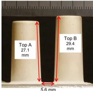
The telecom filter of cast aluminium is pre-plated with zincate treatment, cyanide copper plating and strike silver. Final silver plating is applied to the telecom filter by DC and PR plating by facing an anode of similar size at a distance of 20 cm. Agitation is made by sidewise reciprocating motion of both the telecom filter and the anode with an amplitude of 9 cm at 18 rpm. After plating, the filter is cut in pieces to be able to measure the coating thickness along the gap between the two narrowest tops in the filter (see Fig. 7). Again, the TP is defined as the minimum thickness divided by the average plating thickness.
The experiments on hollow 3D objects and telecom filters are carried out as single experiments and have not been repeated.
Results
Copper platingFigs. 8-9 show copper thickness profiles on Assaf panels plated by DC and PR plating, respectively, using an average current density of 4 A dm-2. The PR plating parameters are jc = 6 A dm-2, ja = 12 A dm-2, tc = 3 s and ta = 1 s. Both plating modes result in semi-bright deposits. The TP is calculated to 0.48 and 0.59 for DC and PR, respectively, showing that TP can be improved by PR plating. It is also seen that the directional flow created by the agitation in the beaker give rise to an asymmetric thickness distribution which is most pronounced at the front of the panels.
When plating the hollow 3D objects using the same DC and PR parameters, the thickness distribution becomes very poor in all experiments. All deposits inside the objects are dull and rough, and it is
meaningless trying to calculate the TP. The very limited agitation inside the objects is suspected to play the main role for the poor quality of the deposits. To test this hypothesis, DC and PR plating on Assaf panels are repeated without agitation. This results in powdery deposits of poor quality. Obviously, it does not work to plate additive-free acid cupper without agitation. Previously reported good results from plating on printed circuit boards using the same additive-free bath had good agitation – also in through holes [17].
Silver plating
The authors of the present paper have recently shown that poor agitation has a positive influence of TP when plating from the same silver bath as in Table 1 [7,18]. A plausible explanation is that cyanide ions not only form complexes with silver ions, they also adsorb to the silver surface of the cathode [19]. When silver deposits by reduction from the cyanide complex, free cyanide ions are released at the cathode surface creating a diffusion layer with cyanide diffusing away from the surface. Free cyanide ions are in equilibrium with adsorbed cyanide ions. As illustrated in Fig. 10, poor agitation increases the surface concentration of adsorbed cyanide, which in turn increases the activation resistance for silver reduction and thereby Wa, resulting in better throwing power. By applying good agitation, the concentration of free cyanide ions at the cathode will approach bulk concentration and the inhibiting effect on silver deposition will be reduced.
In [18] the authors of the present paper have optimized the PR plating parameters to give high TP on the Assaf panel. The optimal parameters are jc = 0.6 A dm-2, ja = 1.2 A dm-2, tc = 400 ms and ta = 80 ms. The resulting average current density is 0.3 A dm-2. Figs. 11-12 show the thickness profiles obtained by optimal PR plating and DC plating at the same average current density. The obtained TPs are 0.96 and 0.85 for PR and DC, respectively.
When plating the hollow 3D objects PR plating parameters are selected using the optimal settings for the Assaf panel as the base. Only ta is allowed to be changed in between 40 to 130 ms, which will change qa/qc between 0.20 and 0.65 and jm between 0.15 and 0.45 A dm-2.
Fig. 13 shows TP vs. current density for DC plating. The TP is shown for the wall and the base plate individually with the purpose to see on which part the minimum is located. For the objects L1 and L3 the coating is thinnest on the base plate and TP reaches optimum values at current densities 0.4 and 0.3 A dm-2, respectively. The result for L9 is different. Here the coating is always thinnest on the deeper part of the wall. For L9, the TP does not pass a maximum, but continue to increase with decreasing current density.
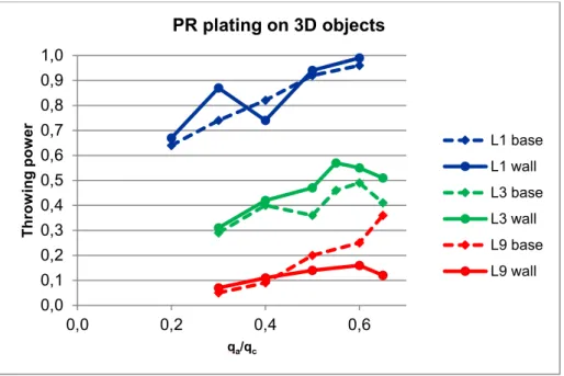
The results from PR plating are shown as TP vs. qa/qc on Fig. 14. For L1 no significant difference is observed between the wall and the base plate. TP increases with qa/qc and reaches values indicating very uniform plating at qa/qc = 0.6. For L3 the base plate is the critical part as in DC plating. The TP passes a maximum of 0.49 for qa/qc = 0.6. Even L9 shows a maximum at qa/qc = 0.6. As in DC plating, the coating is thinnest on the deeper part of the wall. This is clearly a critical region to plate in structures of very high aspect ratio no matter the current mode. Both L3 and L9 show that the TP on the wall drops at high values of qa/qc. This is due to extended anodic dissolution of silver from the upper edge of the wall (reverse dog-bone effect).
DC and PR results are compared in Fig. 15, showing TP vs. jm. It is clearly seen that PR is superior to DC plating in reaching high values of TP. Even for L9 the relative improvement by using PR plating is significant despite the low values. For comparison, the TP results from plating on Assaf panels are also included in the Fig. 15. It is clear that the 3D objects need to be PR plated with higher qa/qc value (resulting in lower jm) than the Assaf panel to reach maximal TP. It has not been possible to establish
a direct correlation factor for TP between the Assaf panel and the 3D objects, but similar trends are observed.
Fig. 16 shows TP vs. jm for silver plating experiments on telecom filters. Again it is confirmed that the TP becomes much better when agitation is avoided. The experiment marked “Ref” is a result from PR plating in an industrial plating line using a proprietary bath composition containing additives. The industrial reference is in line with the laboratory results.
Without agitation, the TP increases slightly by increasing qa/qc (and thereby decreasing jm) until it passes a maximum of 0.71 at qa/qc = 0.55. A sudden drop in TP is observed by further increase in qa/qc. Like for the 3D objects, the drop in TP at high values of qa/qc is caused by extended anodic dissolution on the upper parts of the telecom filter. Again results from plating on the Assaf panel have been included. Like for the 3D objects, the telecom filter needs to be plated with higher qa/qc value than the Assaf panel to reach maximal TP.
Conclusion
The Assaf panel is easy to use and is an efficient tool for evaluating throwing power in electroplating. It is particularly useful for parameter optimization of PR plating when the thickness distribution at the edge is included. One should be aware that the hydrodynamic conditions around the Assaf panel might not be representative for the real plating condition, but usually it is still better than in standard test cells like Hull and Haring-Blum cells.
It has not been possible to establish a direct correlation factor for TP between the Assaf panel and the 3D objects. Nevertheless, the overall trends are the same, making the Assaf panel a useful tool for parametric analysis of baths. Furthermore, the optimal PR parameters for the Assaf panel a good starting point for final object specific parameter optimization.
It has been confirmed that PR plating can improve TP in both acid copper with simple metal ions and cyanide silver plating with strong comploexation. Acid copper plating without additives is negatively affected by insufficient agitation. The situation is the opposite for cyanide silver plating, where no or limited agitation results in improved TP. This is probably due to increased polarization resistance caused by adsorbed cyanide on the cathode surface.
Reference:
1 D.R. Gabe, Test cells for plating, Metal Finishing 2007, 105, (10), 511-517. 2 H.E. Hering and W. Blum, Trans. Am. Electrochem. Soc. 1923, 44, 313-345.
3 C. Madore and D. Landolt, The Rotating Cylinder Hull Cell: Design and Application, Plating & Surface Finishing, 1993, 80, (11), 73-78.
4 C. Madore, D. Landolt, C. Hassenpflug and J.A. Hermann Application of the Rotating Cylinder Hull Cell to the Measurement of Throwing Power and the M onitoring of Copper Plating Baths, Plating & Surface Finishing, 1995, 82, (8), 36-41.
5 P. Leisner, G. Bech-Nielsen and P. Møller, Throwing power in pulse reverse plating from an acid copper bath, proceedings of Sur/Fin’92, Atlanta 22-26 June 1992, Session S: Finishing for printed circuit manufacturing.
6 D.R. Gabe, M. Ward, Y. Assaf, Throwing Power Measurement: The Assaf Cell, Plating and Surface Finishing 2001, 88, (5), 127-130.
7 P. Leisner, C. Zanella, I. Belov, C. Edström and W. Hui, Influence of anodic pulses and periodic current reversion on electrodeposits, Transactions of the Institute of Metal Finishing 2014, 92, (6), 336-342. 8 Y. Assaf, Finishing tip of the month. Distribution of Metal Thickness – A New Cell and an Experiment,
9 Y. Assaf, A new test for determining throwing power factor and improving covering power, Metal Finishing 2002, 100, (8), 12, 14.
10 P.T. Tang, Fabrication of Micro Components by electrochemical deposition, PhD Thesis, Technical University of Denmark 1998.
11 E. Malyshev, U. Landau and S. Chivilikhin, Modeling the deposit thickness distribution in copper electroplating of semiconductor wafer interconnects, AIChE annual meeting ’03, Nov. 16-21, 2003, San Francisco, Paper 190.
12 G. Nelissen, R. Belis, Advanced Simulations of Copper Layer Thickness Distribution on Printed Circuit Boards, Metal Finishing, 2009, 107, (3), 27-29.
13 R.W. Pryor, A 2D Axisymmetric Electrodeposition Model, 2011 COMSOL Conference, Boston, Oct. 13-15, 2011.
14 I. Belov, C. Zanella, C. Edström and P. Leisner, Finite element modeling of silver electrodeposition for evaluation of thickness distribution on complex geometries, Materials and Design 2016, 90, 693-703. 15 C. Wagner, The Scope of Electrochemical Engineering, in Advances in electrochemistry and
electrochemical engineering, by C.W. Tobias (Ed.), Interscience Publishers 1962.
16 N. Ibl, Transport Phenomena in electrolytic systems, in Information Bulletin – Number 59, IUPAC, July 1977.
17 P. Leisner, P. Møller & A. McNelly, Throwing power and ductility of pulse reversal plated copper for PCBs, Processing of Advanced Materials 1994, 9, 148-154.
18 P. Leisner, C. Zanella, I. Belov, C. Edström, G. Sandulache, W.E.G. Hansal, Control of silver throwing power by pulse reverse plating, Transactions of the Institute of Metal Finishing 2017, 95, (1), 25-30.
Figures
Figure 1: Top-view of Haring-Blum cell showing the asymmetric location of the anode between two cathodes
Figure 2: Bended cathode sheet
Figure 3: The Assaf panel in it’s original design Figure 4: Circular Assaf panel
Figure 5: Relationship between slope of the polarization curve and TP. A high slope, which is obtained at low current density results in relative good TP.
Figure 6: Hollow 3D test objects with removable side wall and base. All dimensions are in mm
Figure 7: Telecom filter. Coating thickness is measured around the narrow gab between top A and B. TP is defined as minimum thickness along the red arrows divided by the average plating thickness Figure 8: Thickness distribution of cupper on Assaf panel plated by DC at 4 A dm-2
Figure 9: Thickness distribution of cupper on Assaf panel plated by PR at jm = 4 A dm-2
Figure 10: Illustration of how the surface concentration of cyanide depends on agitation. By natural convection (blue) the diffusion layer is thick, resulting in high surface concentration of cyanide. By stirring (red) the diffusion layer becomes narrower and the surface concentration of cyanide becomes lower.
Figure 11: Thickness distribution on Assaf panel by optimal PR plating with jm = 0.3 A dm-2 and no
agitation
Figure 12: Thickness distribution on Assaf panel by DC plating at 0.3 A dm-2 and no agitation Figure 13: TP on hollow 3D structures plated by DC at different current densities
Figure 14: TP on hollow 3D structures plated by PR with different qa/qc
Figure 15: Summary of TP on 3D structures. Results from Assaf panels are inserted for comparison Figure 16: TP vs jm by silver plating on telecom filter. The experimental points are labeled with the qa/qc value. The result marked “Ref” is plated in an industrial line with additives. Results from Assaf panels are inserted for comparison
Fig. 5
│η│
│j│
High dηa/dja ⇒ good TP
Fig. 6
15
15 (outer measure)
15
135
136
20
15
Mounting
onto a back
panel
15
15 (outer measure)
15
45
46
20
15
Mounting
onto a back
panel
15
15 (outer measure)
15
15
16
20
15
Mounting
onto a back
panel
L9
Fig. 7 Top B 29.4 mm Top A 27.1 mm 5.6 mm
Fig. 8 0 2 4 6 8 10 -20 -10 0 10 20 Th ickn ess /µ m
Distance from centre /mm
Cu DC: 4 A dm-2
Front Back
Agitation Direction
Fig. 9 0 2 4 6 8 10 -20 -10 0 10 20 Th ickn ess /µ m
Distance from Centre /mm
Cu: PR jm= 4 A dm-2
Front Back
Agitation Direction
Fig. 10
Bulk conc of CN
-Bulk conc of Ag(CN)3 2-CN-ad ↔ CN
-e- + Ag(CN)32
-→ Ag + 3 CN
-Diffusion layer thickness
by stirring Diffusion layer thickness by natural convection
Conc.
Fig. 11 0 2 4 6 8 10 12 -20 -10 0 10 20 Th ickn ess
Distance from centre /mm
Ag PR: jm= 0.3 A dm-2
Front Back
Fig. 12 0 2 4 6 8 10 12 -20 -10 0 10 20 Th ickn ess
Distance from centre /mm
Ag DC: 0.3 A dm-2
Front Back
Fig. 13 0,0 0,1 0,2 0,3 0,4 0,5 0,6 0,7 0,8 0,9 1,0 0,0 0,1 0,2 0,3 0,4 0,5 Th ro w in g p ow er Current density /A dm-2 DC on 3D objects L1 base L1 wall L3 base L3 wall L9 base L9 wall
Fig. 14 0,0 0,1 0,2 0,3 0,4 0,5 0,6 0,7 0,8 0,9 1,0 0,0 0,2 0,4 0,6 Th ro w in g p ow er qa/qc PR plating on 3D objects L1 base L1 wall L3 base L3 wall L9 base L9 wall
Fig. 15
(Assaf results are now visible)
0,0 0,1 0,2 0,3 0,4 0,5 0,6 0,7 0,8 0,9 1,0 0,0 0,1 0,2 0,3 0,4 0,5 Th ro w in g p ow er
Average current density /A dm-2
DC and PR on 3D objects L1 PR L1 DC L3 PR L3 DC L9 PR L9 DC
•
Assaf PR•
Assaf DCFig. 16
(Assaf results are now visible)
0.00 0.30 0.40 0.50 0.55 0.60 0.00 0.30 Ref. 0.30 0,0 0,1 0,2 0,3 0,4 0,5 0,6 0,7 0,8 0,9 1,0 0,0 0,1 0,2 0,3 0,4 0,5 Th ro w in g P ow er
Average current density /A dm-2
Throwing Power on telecom filter
Still Agitation