Postprint
This is the accepted version of a paper published in Physica Status Solidi (a) applications
and materials science. This paper has been peer-reviewed but does not include the final
publisher proof-corrections or journal pagination.
Citation for the original published paper (version of record):
Adamczyk, K., Søndenå, R., You, C C., Stokkan, G., Lindroos, J. et al. (2017)
Recombination Strength of Dislocations in High-Performance
Multicrystalline/Quasi-Mono Hybrid Wafers During Solar Cell Processing
Physica Status Solidi (a) applications and materials science, : 1700493
https://doi.org/10.1002/pssa.201700493
Access to the published version may require subscription.
N.B. When citing this work, cite the original published paper.
Permanent link to this version:
Recombination strength of dislocations in high-performance
multicrystalline/quasi-mono hybrid wafers during solar cell
processing
Krzysztof Adamczyk *,1, Rune Søndenå2, Chang Chuan You2, Gaute Stokkan3, Jeanette Lindroos4,
Markus Rinio4, and Marisa Di Sabatino1
1 Department of Materials Science and Engineering, NTNU, A. Getz vei 2B, NO-7491 Trondheim, Norway 2 Department for Solar Energy, IFE, NO-2007 Kjeller, Norway
3 Sintef Materials and Chemistry, NO-7465 Trondheim, Norway 4 Karlstad University, 651 88 Karlstad, Sweden
Keywords Silicon, Solar cell, Gettering, Hydrogenation, Dislocations
Wafers from a hybrid silicon ingot seeded in part for High Performance Multicrystalline, in part for a quasi-mono structure, were studied in terms of the effect of gettering and hydrogenation on their final Internal Quantum Effi-ciency. The wafers were thermally processed in different groups – gettered and hydrogenated. Afterwards, a low temperature heterojunction with intrinsic thin layer cell process was applied to minimize the impact of temperature. Such procedure made it possible to study the effect of dif-ferent processing steps on dislocation clusters in the mate-rial using the Light Beam Induced Current technique with
a high spatial resolution. Dislocation densities were meas-ured using automatic image recognition on polished and etched samples. Dislocation recombination strengths were obtained by a correlation of the IQE with the dislocation density according to the Donolato model. Different clus-ters were compared after different process steps. The re-sults show that for the middle of the ingot, the gettering step can increase the recombination strength of disloca-tions by one order of magnitude. Subsequent passivation with layers containing hydrogen can lead to a decrease in the recombination strength to levels lower than in unget-tered samples.
1 Introduction Crystalline silicon maintains its status
as the main material used in solar cells. The latest reports show that multicrystalline silicon has gained more ground in the last years and made up 70% of the market in 2016 [1, 2]. While the Czochralski (CZ) crystallization technique provides high-quality monocrystalline material leading to higher cell efficiencies, the directional solidification of mul-ticrystalline ingots allows for higher throughput and lower production costs, offsetting its lower efficiency [3, 4]. Still much effort is aimed at decreasing the negative effect of structural defects on the device performance [5, 6]. One ap-proach is to control the structure of the final ingot by chang-ing the nucleation phase, such as growchang-ing Quasi-Mono (QM) silicon [7] or High Performance Multicrystalline (HPMC) ingots [8]. Quasi-mono growth requires a seeding layer consisting of monocrystalline silicon slabs of specific orientation, which are laid out next to each other and melted partially, before the ingot starts to crystallize. This approach leads to a crystalline structure replicating that of the seeds. Defects originate from the joints between the seeds and from grains nucleated on the crucible walls [9, 10].
Seeding can also be used to grow HPMC-Si, e.g. by flu-idized bed reactor Si feedstock [6, 8, 11, 12]. This method
* Corresponding author: e-mail krzysztof.adamczyk@ntnu.no, Phone: +47 415 419 94
results in a structure with grains smaller than in standard multicrystalline silicon. HPMC-Si also contains an in-creased number of random angle grain boundaries, in con-trast to standard multicrystalline ingots that are dominated by Σ3 Coincidence Site Lattice grain boundaries. Random angle grain boundaries were shown to be more detrimental to performance than Σ3 boundaries, since they are more heavily decorated with impurities [13-16]. However, in HPMC, random angle grain boundaries offset some of their own recombination activity by annihilating dislocations [17]. This leads to increased performance in HPMC cells, when compared with the standard multicrystalline cells that contain higher densities of efficiency-limiting dislocations [18].
The effect of defects and impurities present after crys-tallization on cell performance can be mitigated during cell processing through impurity gettering and defect pas-sivation. Both grain boundaries and dislocations present in the material are less harmful when clean, but their negative effect increases with impurity decoration [14, 19]. Gettering can be used to introduce sinks for fast diffusing metallic im-purities, such as Fe, Ni or Cu, into the noncritical parts of the device [16, 20-24]. A subsequent technique in the solar
cell production chain, hydrogen passivation or hydrogena-tion for short, passivates part of the metallic impurities and dangling bonds of the crystal lattice near structural defects, resulting in an increased minority carrier lifetime [25-30]. Even though gettering and hydrogenation are applied in standard solar cell manufacturing, the HPMC-Si material is still limited in efficiency by defects, particularly by disloca-tions [17, 18]. The effect of dislocadisloca-tions on the recombina-tion of minority charge carriers was modeled by Donolato with a parameter describing the recombination strength γd,
normalized to a dimensionless parameter Γ= γd /D, where D
is the minority carrier diffusion coefficient [31]. γd is the
number of recombinations per time, the dislocation length, and the excess carrier density [32]. The normalized value of this parameter G serves as a measure of the recombination strength of dislocation clusters. Rinio et al. showed that the effect of dislocations on the cell efficiency depends on their spatial pattern [32]. An interesting observation was that larger recombination strengths were typically found at dis-location clusters with random arrangement, while lower re-combination activity is seen at clusters of ordered and aligned dislocations. The difference has been explained to result from different evolution and structures of the disloca-tions after crystal growth, with or without recovery and polygonization [33]. Polygonization, a process where dislo-cations arrange in low energy structures by glide and climb processes, leads to a certain degree of ordering. The tensile stress field of a dislocation aligns with the compressive stress field of its neighbouring dislocation, reducing the strain. This process can be expected only at higher temper-atures because it requires climb and glide. It is possible that after polygonization the dislocations have a lower gettering strength as a result of a smaller number of kinks and jogs on the dislocations in ordered structures and a weaker stress field around them, which both lead to a higher precipitate nucleation energy barrier.
The question how dislocation clusters in HPMC-Si react to gettering and hydrogenation requires further work in or-der to reduce their effect on device performance. This study aims to analyze this issue in terms of recombination strength in HPMC-Si. A hybrid ingot, consisting of both HPMC and quasi-mono silicon, is used to investigate this effect. The quasi-mono part serves as a reference material grown in the same crystallization process as the HPMC part, but without the effect of grain boundaries.
2 Experimental methods
2.1 Ingot growth A hybrid ingot with an approximate
diameter of 25 cm and a weight of 15 kg was grown with a Crystalox DS 250 directional solidification furnace. Boron was added to achieve a resistivity of about 1.0-1.3 Ω·cm. The ingot structure was defined by placing a seeding layer on the bottom of a high-purity quartz crucible coated with Si3N4. Such a crucible is normally only used for CZ growth,
but it was chosen for this directional solidification experi-ment, in order to obtain an ingot purity comparable to the industrial quality in a pilot scale furnace.
The quasi-mono part of the ingot was seeded by placing two slabs cut from a CZ ingot in [100] orientation over one half of the crucible bottom as shown in Fig. 1. a) and b). The other half was filled with Fluidized Bed Reactor (FBR) granules up to the CZ slab level to seed the HPMC part. The whole crucible was filled with high purity feedstock. During the melting, a quartz rod was used to probe the solid-liquid interface to check that the seeding structure had melted only partially, allowing for seeded growth in both parts of the crucible. The result was a hybrid ingot consisting of HPMC and quasi-mono. Additional details on ingot growth can be found in [34]. After growth a slab containing the seeds, of about 3 cm thickness was cut off from the bottom of the in-got and from the remaining part a 156 mm x 156 mm block was cut, according to the scheme in Fig. 1 b). The resulting block had about 10 cm height. The block was grinded and industrially wafered into 180 µm thick hybrid wafers.
2.2 Wafer & cell processing The wafers were
di-vided into groups and processed according to the scheme in Fig. 2. Industrial reference HPMC-Si material was added to each respective group. All groups were first damage etched in a HF:Nitric acid:Acetic acid solution (CP5) and cleaned. The ungettered (U) group was only etched and cleaned after wafering. The gettered (G) group underwent a phosphorus in-diffusion process (PDG) in about 830 °C where POCl3
gas was used as a phosphorus source to create a 75 Ω /sq. emitter. In the third group, gettered and hydrogenated (G+H), PDG was followed by surface passivation with a hy-drogen-rich SiOxNy/SiNx stack layer using
plasma-en-hanced chemical vapor deposition (PECVD). The SiOxNy
layer was deposited at 130 °C and capped with SiNx
3
Figure 1 a) Seeding structure for the hybrid ingot. b) Top view of
the seeding structure with an overlaid block cutting scheme (red lines), and the orientation of the seeding with CZ slabs. c) The grown hybrid ingot in its crucible. d) Minority carrier lifetime map (PL) of an ungettered, but surface-passivated wafer (156 mm x 156 mm) cut from the middle of the ingot. Dashed lines on the PL map show the 50 x 50 mm areas, which were cut from the full wafers and processed into HIT cells for LBIC measurements.
Figure 2Processing steps for three groups of full (156 mm x 156
mm) hybrid wafers.
With layers deposited in such manner the wafers were subsequently hydrogenated through a standard high-temper-ature contact firing process, with a 720 °C peak temperhigh-temper-ature. Finally, all the wafers were etched in a fresh CP-5 solution to remove a layer thicker than the emitter in the G and G+H
groups. Some sister wafers from all three groups were pas-sivated on both sides with amorphous Si layers (about 40 nm thick) by PECVD at about 230 °C for lifetime measure-ments. Other sister wafers were cut into 50 mm x 50 mm samples and processed further into Heterojunction with In-trinsic Thin layer solar cells (HIT) [35] for LBIC measure-ments. The HIT structure with its low-temperature pro-cesses (< 200 °C) was chosen to prevent thermally induced changes to the bulk recombination activity in all three wafer groups. The HIT process consisted of subsequent PECVD of different layers: amorphous intrinsic Si, n-type or p-type doped amorphous Si, and indium-wolfram oxides as a trans-parent conducting film [36]. The a-Si layers were approxi-mately 10 nm thick, the IWO layer had about 80 nm on the front and 70 nm on the backside. The Ag contacts were printed using the same mesh on both the front and the back sides, to create overlapping contacts with minimal effect on the LBIC signal. Following electrical characterization, the HIT cells contacts were removed by etching in aqua regia at 80 °C for 2 h, followed by mechanical polishing. The pol-ished samples were selectively etched in the Secco etchant for 60 s [37] to obtain optimal etch pit size.
2.3 Characterization The wafer set for lifetime
meas-urements was characterized by band-to-band photolumines-cence (PL) imaging during uniform illumination with a 808 nm laser, calibrated with quasi-steady state photoconduct-ance measurements on an LIS-R1 instrument from BTIm-aging [38, 39]. The average minority carrier lifetime was determined at one sun light intensity corresponding to a con-stant carrier generation rate of 1.13E19 cm-3s-1.
The HIT samples were first characterized using a custom-built LBIC system with a 826 nm laser as excitation source, with resolution of 12.5 µm and about 2 µW light power [32] to obtain maps of the internal quantum efficiency (IQE). Mi-croscopic images were measured in an array using an auto-mated optical microscope (Olympus MX61A) combined with the ImageJ analysis software to measure the positions of etch pits [40]. Based on this, topograms of the dislocation density with a resolution identical to the IQE topograms of the same area were calculated [41] to allow for a direct pixel by pixel comparison of EPD and IQE [42]. The carrier dif-fusion length and dislocation density were related by the Donolato model, with the recombination strength as a fitting parameter [31, 32]. IQE was related to the carrier diffusion length in the cell through a simple PC1D model [43]. The HIT-like cells were modelled assuming a shallow emitter with about 2.9x1020 cm-3 peak doping on an Erfc profile and
a front surface recombination velocity of 1000 cm/s. The rear surface recombination was fitted to the highest IQE val-ues measured in the cells. Plots of IQE as a function of etch pit density were drawn and fitted with the Donolato recom-bination model for the analysed dislocation clusters. The re-combination strength of the dislocations was extracted from curve fitting of each dislocation cluster.
The impurity content in the ingot was measured by Neutron Activation Analysis (NAA) at the Missouri University Re-search Reactor. A precise measurement with this technique required relatively large, roughly cubic pieces of material with a 20 mm edge. The results presented in this work come from a piece of the HPMC part of the ingot, which was cut out next to the 156 mm x 156 mm block at 44 to 66% of fraction solidified. The error of NAA for each element is given with the respective results. The segregation of impu-rities into the dislocation clusters was analysed by Second-ary Ion Mass Spectrometry (SIMS) on a Cameca IMS 7F measurement system. This system allowed studying the im-purity content in selected circular areas with a diameter of about 60 µm. The SIMS measurement error was at its high-est 10% of the measured value and it originated from an in-strument error along with the uncertainty in the implanted dose of the reference sample.
3 Results and discussion
3.1 General trends The average minority carrier
re-combination lifetimes (lifetimes for short) obtained from PL measurements and shown in Fig. 3 indicate that the QM part of the ingot has higher lifetimes than the HPMC part in all three wafer groups at all ingot heights. What can also be seen for both QM and HPMC is that the bottom and top parts of the ingot show reduced lifetime values, with the lowest values in the bottom. This should be attributed to the impu-rity distribution in the ingot, i.e., the red zone effect related to both segregation during crystal growth, and diffusion of impurities from the crucible walls during cooling of the in-got. An interesting observation is that this effect is much stronger in the HPMC part, where a high density of defects is present, possibly allowing for faster diffusion in the ingot [44, 45].
Gettering is also less efficient in the HPMC part. In the upper part of the ingot, gettering of HPMC even results in a decrease of the mean lifetime, similar to a previous study on commercially available multicrystalline wafers [46]. It has been shown that such a deterioration of the wafers by get-tering typically can take place at the extended defects. In line with recent reports an additional hydrogenation step is required to obtain an improvement to values higher than in the ungettered state in the top and middle of the ingot [15, 47, 48]. The situation is different in the bottom wafers, as gettering alone improves the mean lifetime, probably be-cause of the higher initial impurity content. In the QM part, the gettering process increases the mean lifetime for each position. Hydrogenation slightly increases the mean lifetime even further. This is because the QM part of the ingot has a low density of extended defects (grain boundaries, disloca-tions) when compared with the HPMC part. The detailed study of how the dislocation recombination strength changes after each process step and affects the electrical per-formance of the device has been performed by LBIC meas-urements and is presented below for different ingot posi-tions.
Figure 3Average lifetimes from QSSPC calibrated PL
measure-ments for both HPMC and Quasi Mono parts of the wafers along the ingot height.
3.2 HPMC – bottom of ingot In the bottom of the
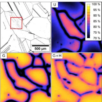
ingot, on samples from about 10% relative ingot height, dis-location clusters were too few to allow for quantification of their recombination strength. The dislocations that were available for analysis were found too close to grain bound-aries, their effect on IQE was also too low to extract any data allowing a fit with the Donolato curves. The IQE maps al-lowing for a qualitative comparison are presented in Fig. 4. The main observation, already mentioned, is that even with relatively large dislocation densities, about 8x105 cm-2 in the
case of the area marked in Fig. 4, the effect of dislocations on the overall performance seems small when compared to the effect of grain boundaries. In the ungettered state, the IQE in high dislocation density areas is higher than in neigh-bouring grains with dislocation densities below 104 cm-2.
The IQE in the ungettered state is overall much smaller than after subsequent process steps. The major difference occurs in areas of low densities of extended defects, where values of about 70% are measured in the middle of the grains in the ungettered state, while in the gettered and gettered and hy-drogenated the same areas show values of about 95%. This shows that PDG can be an efficient way of improving the efficiency of samples from the red zone area of the ingot.
3.3 HPMC – middle of ingot The middle of the ingot
contains dislocation clusters that are recombination-active enough for quantification. Fig. 5 shows the recombination strength of dislocation clusters in the middle and top of the hybrid ingot and in the middle of an industrial HPMC refer-ence ingot. Dislocations from the HPMC part of the hybrid ingot grown in laboratory scale furnace show very similar recombination strength values to the ones observed in indus-trial reference.
The main trend is a considerable increase in dislocation recombination strength after gettering and a subsequent re-duction by hydrogenation. This is in agreement with the life-time measurements, where gettering causes only a relatively small improvement or even deterioration of the measured average value.
5
Figure 4Micrograph of dislocation structures in the bottom of the
ingot and IQE maps of the neighboring wafers after different pro-cessing. The micrograph has been processed with ‘make binary’ and ‘dilute’ ImageJ algorithms for presentation purposes. The dis-location density measured in the area marked with a red square is about 8x105 cm-2.
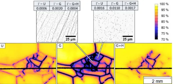
IQE maps of a larger dislocation structure from the middle of the ingot can be seen in Fig. 6. These maps show that while the signal from low defect density areas is im-proved during gettering, with an increase from about 96 %
to 98 %, recombination at crystal defects increases consid-erably. The improved performance of the hydrogenated cell can be attributed to a decrease of recombination at grain boundaries and dislocations, while maintaining the higher bulk lifetime gained during gettering. As mentioned, there is also a difference between the dislocation clusters that are visible especially after gettering but also present after other process steps. The top row of Fig. 6 presents two clusters with different dislocation distributions. The cluster on the left shows a type of ordered dislocations, while the right cluster is unordered. Both of these clusters have a similar dislocation distribution on the neighbouring wafers. When comparing the recombination strength of these clusters, it can be noted that after every process step, the dislocations distributed randomly show higher recombination activity, even though the dislocation density in the ordered cluster is considerably larger. This is in agreement with previous, similar work performed on standard multicrystalline silicon material [32].
3.4 HPMC – top of ingot The top part of the ingot
differs from the middle in terms of much lower mean life-time values after gettering (G), as seen in Fig. 3. Neverthe-less, lifetime recovery and improvement were possible through hydrogenation (G+H). This effect can also be seen in IQE maps, presented in Fig. 7. The difference in the IQE scale should be noted, when comparing the top maps to other ingot positions. The effect of gettering on recombina-tion activity of the defects was considerably stronger, and while values of about 70% IQE were measured on high dis-location density areas in the middle of the ingot, in the top
Figure 5The recombination strength of dislocation clusters in the hydrid ingot and an industrial HPMC ingot
after different processing steps. The results for different gamma values are presented in terms of a box plot: for each group the middle line is the median, the box contains 50% of the population centered on the median, and the whiskers show the upper and lower quartiles.
these levels nearly reached 0%, especially in larger disloca-tion structures like the one visible in Fig. 7. The recombina-tion strength of dislocarecombina-tions in the top is similar to the mid-dle ingot part in ungettered (U) and fully processed (G+H) states in Fig. 5. In the gettered state, however, the recombi-nation activity of dislocations is higher in the top than in the middle of the ingot.
3.5 Quasi-mono In the middle of the quasi-mono part,
the only extended defects are dislocation clusters originating from the horizontal seed joint. These clusters are visible in the PL map in Fig. 1 d. Figure 8 shows a fine resolution IQE map of this area on neighbouring wafers. Dislocation struc-tures originating at the seed junction are visible after all pro-cess steps. The low defect density areas in the ungettered sample show relatively lower IQE than in the gettered and fully processed samples. The IQE contrast and recombina-tion strength of the dislocarecombina-tions is relatively high in the un-gettered state, higher than in HPMC. The increase in Γ of dislocation clusters in the QM part during gettering is not as strong as in HPMC, indicating an increased efficacy of the gettering process in the QM part. This may be caused by a lower defect density in this part of the ingot, resulting in a an overall lower concentration of impurities trapped on these defects. A lower density of defects, acting as nuclea-tion sites for precipitates during gettering, also allows for a more efficient gettering process. The precipitates present in the material before gettering can dissolve more easily, al-lowing also more of the impurities to diffuse to the gettering layer. This leads to a better performance after hydrogenation and lower Γ-values after full processing, even though only the unordered dislocation clusters were found in this part of the ingot. Another important factor is that during the ingot
growth the incorporation of impurities in the QM part is probably slower than in the HPMC part due to the differing defect densities. Such a factor would affect both the perfor-mance of the ungettered samples, as well as the IQE/lifetime levels after gettering.
Figure 7A binarized and diluted micrograph and IQE maps of
areas on samples from neighbouring wafers from the top of the in-got. A large dislocation structure can be seen in the images. The dislocation density in the middle of the visible grain reached 4x10⁶
cm-2. Note the differences in the IQE scale when compared to other
maps presented in this work.
Figure 6Bottom row - IQE maps of a high dislocation density structure on neighbouring wafers after different
process steps. Top row - micrographs of selected dislocation clusters from this structure are presented along with their Γ-values. Dislocation densities for the ordered cluster on left and unordered on the right are 7x10⁶
7
3.6 Impurity concentration Since impurity
decora-tion is known to determine the dislocadecora-tion recombinadecora-tion strength after various process steps, their concentration in the material and segregation to defects was assessed with NAA and SIMS. The mean concentration of impurities in the ungettered material was measured with NAA on a large, 20x20x20 mm3 sample. It revealed that the ingot was
rela-tively pure. The only transition metals found in concentra-tions above the detection limit are listed in Table 1. Table 2 presents the detection limits of other expected impurities.
Figure 8IQE maps of areas on samples from neighbouring wafers
from the QM part from the middle of the ingot. Dislocation struc-tures originating at the seed joint are visible along a horizontal line in the middle of the maps.
Table 1 Impurity concentrations found in the ingot by NAA.
Given in atoms/cm3.
Co Cr Ni Zn
2.2±2 x10¹⁰ 2.6±0.04 x10¹² 2.3±0.08 x10¹³ 2.8±0.4 x10¹¹
Table 2Detection limits of impurities not found by NAA. Given
in atoms/cm3.
Fe Cu K Ti Mo
2.3 x10¹² 7.1 x10¹² 5.5 x10¹² 6.7 x10¹⁴ 4.4 x10¹¹
While NAA only detected the mean impurity concentrations in relatively large volumes of the unprocessed wafers, SIMS was used to measure the impurity concentration in and the impurity segregation towards dislocation clusters, enclosed within a sputtered area of about 60 µm in diameter. Ungettered and gettered samples were analysed by SIMS, but only Ni was detected due to poor detection limits. Changes in impurity distribution during hydrogenation by firing were not
expected to be large enough to allow for detection. Figure 9 shows the Ni concentration per cluster along with two depth profiles on one of the analysed clusters. In the ungettered middle of the ingot, a clear difference is seen between the mean Ni bulk concentration of 2.3±0.08 x10¹³ atoms/cm3
(NAA) and the Ni concentration in the dislocation clusters in the order of 1016 atoms/cm3 measured by SIMS. This
indicates a strong impurity gettering of fast-diffusing Ni [49] from the bulk towards the dislocations, during the ingot cooling. Even though interstitial Ni is harmless, it is unstable and prefers to precipitate at extended defects, forming recombination-active NiSi2 [50]. After PDG, the Ni
concentration is even higher in the dislocation clusters, showing strong collection of Ni to the dislocations during PDG. Therefore, increased Ni precipitation might explain the increase in the recombination strength of the dislocation clusters after gettering in Fig. 5. Nickel precipitates can also be readily passivated by hydrogen, which could partly explain the decreased recombination activity after gettering and hydrogenation [51]. In the ingot top, the Ni concentration at the dislocations in the ungettered state is relatively larger than in the middle. We can probably assume that also other harmful elements like Fe should be present in higher, but still undetectable concentrations. In the case of the top samples, impurities could then diffuse to the dislocations from a smaller volume and still affect their recombination strength. Considering this, elements diffusing in silicon slower than Ni could be the reason for the very high recombination strength of dislocations in the gettered samples in the top of the ingot. Another possible explanation of the increase of recombination strength during the gettering process is a change in the precipitate distribution [50]. The depth profiles of Ni presented in Fig. 9 indicate this. Two peaks were found in the depth profile of one of the clusters with higher recombination strength, each about 0.8 µm wide. They possibly came from large precipitates or precipitate agglomerates on this cluster. A lack of similar peaks in the profile from the gettered sample might mean that while the impurity content was similar, the size of precipitates at these dislocations was different, leading to different recombination mechanisms and differences in recombination strength. Such explanation is based only on a profile obtained from one out of ten analysed dislocation clusters. If a change in precipitate distribution occurred on the other clusters as well, it was not detected.
The SIMS measurements aimed also at analysing the ordered and disordered dislocation clusters in terms of impurity concentration, but no significant differences were found.
4 Conclusions Overall the recombination strength of
dislocations Γ is increased by an order of magnitude during the gettering process, often leading to a decreased material performance in the gettered state. Subsequent hydrogena-tion reduces the recombinahydrogena-tion strength to levels lower than
in the ungettered state. Both processes are necessary to ob-tain optimal device performance.
In the bottom of the ingot there are few dislocation clus-ters and their recombination activity is affecting the material performance much less than grain boundaries. The disloca-tions and the effect of thermal processing on these are largely negligible in the bottom wafers.
Dislocations are present in higher densities in the middle and top of the ingot. A difference in recombination strength between unordered and ordered dislocation clusters was found, where the unordered clusters exhibit higher Γ values.
While such difference has been previously shown in standard mc-Si, this work shows that it also exists in HPMC-Si. There are various explanations for this effect, but they highlight the possible difference in impurity segregation to-wards ordered and unordered dislocations.
The effect of segregation plays an important role in de-fining the recombination activity, which could explain the difference in recombination strength between the gettered clusters in QM and HPMC parts. The decreased density of internal gettering sites in the QM might result in a larger amount of impurities being internally gettered to disloca-tions, and thus in a higher recombination strength of dislo-cations in this part of the ingot.
The role of impurity segregation and precipitate distri-bution for device performance is confirmed by the SIMS measurements of impurity concentration at different dislo-cation clusters.
Acknowledgements The work reported in this paper
was performed in the project Impurity Control in High Per-formance Multicrystalline Silicon, 228930/E20, funded by the Norwegian Research Council’s ENERGIX programme and industry partners REC Solar, REC Silicon, Steuler Solar and The Quartz Corp. Part of this work was also supported by the SOPHIA project "HPSS", the Solar-Era.Net project "HighCast" via the Swedish Energy Agency, and the project
"Advanced analysis of industrial silicon wafers for solar cells" by J. Gust. Richert stiftelse, which is gratefully acknowledged.
References
[1] Fraunhofer Institute for Solar Energy Systems, Photovoltaics Report, 2016.
[2] Fraunhofer Institute for Solar Energy Systems, Photovoltaics Report, 2017.
[3] L. Arnberg, M. Di Sabatino, E.J. Øvrelid, State-of-the-art growth of silicon for PV applications, Journal of Crystal Growth 360(2012) (2012) 56-60.
[4] L. Arnberg, M. Di Sabatino, E. Øvrelid, Solidification of Silicon for Solar Cells, Transactions of the Indian Institute of Metals 65(6) (2012) 509-513.
[5] M. Di Sabatino, G. Stokkan, Defect generation, advanced crystallization, and characterization methods for high-quality solar-cell silicon, physica status solidi (a) 210(4) (2013) 641-648.
[6] G. Stokkan, A. Ciftja, Growth of High Performance Multicrystalline Silicon; A Literature Review, SINTEF Materials and Chemistry, 2014.
[7] N. Stoddard, B. Wu, I. Witting, M.C. Wagener, Y. Park, G.A. Rozgonyi, R. Clark, Casting Single Crystal Silicon: Novel Defect Profiles from BP Solar's Mono2 Wafers, Solid State Phenomena 131-133 (2008) 1-8.
[8] C.W. Lan, A. Lan, C.F. Yang, H.P. Hsu, M. Yang, A. Yu, B. Hsu, W.C. Hsu, A. Yang, The emergence of high-performance multi-crystalline silicon in photovoltaics, Journal of Crystal Growth (2016).
[9] M. Trempa, C. Reimann, J. Friedrich, G. Müller, D. Oriwol, Mono-crystalline growth in directional solidification of silicon with different orientation and splitting of seed crystals, Journal of Crystal Growth 351(1) (2012) 131-140.
[10] K.E. Ekstrøm, G. Stokkan, R. Søndenå, H. Dalaker, T. Lehmann, L. Arnberg, M. Di Sabatino, Structure and
Figure 9SIMS measurement results. a) Nickel concentration at dislocation clusters, numbered from 1 to 10, in the middle and the top samples.
b) Nickel depth profiles in a cluster in top of the ingot. For the remaining analysed cases, the depth profiles were flat like the ungettered profile,
9
dislocation development in mono-like silicon, physica status solidi (a) 212(10) (2015) 2278-2288.
[11] C.W. Lan, W.C. Lan, T.F. Lee, A. Yu, Y.M. Yang, W.C. Hsu, B. Hsu, A. Yang, Grain control in directional solidification of photovoltaic silicon, Journal of Crystal Growth 360 (2012) 68-75.
[12] K.E. Ekstrøm, G. Stokkan, A. Autruffe, R. Søndenå, H. Dalaker, L. Arnberg, M. Di Sabatino, Microstructure of multicrystalline silicon seeded by polysilicon chips and fluidized bed reactor granules, Journal of Crystal Growth 441 (2016) 95-100.
[13] J. Chen, T. Sekiguchi, D. Yang, F. Yin, K. Kido, S. Tsurekawa, Electron-beam-induced current study of grain boundaries in multicrystalline silicon, J. Appl. Phys. 96 (2004).
[14] J. Chen, T. Sekiguchi, Carrier Recombination Activity and Structural Properties of Small-Angle Grain Boundaries in Multicrystalline Silicon, Japanese Journal of Applied Physics 46(10A) (2007) 6489-6497.
[15] K. Adamczyk, R. Søndenå, M. Mhamdi, A. Autruffe, G. Stokkan, M. Di Sabatino, Grain boundary effect on lifetime in high performance multicrystalline silicon during solar cell processing, physica status solidi (c) 13(10-12) (2016) 812-815.
[16] M.S. Wiig, K. Adamczyk, H. Haug, K.E. Ekstrøm, R. Søndenå, The Effect of Phosphorus Diffusion Gettering on Recombination at Grain Boundaries in HPMC-Silicon Wafers, Energy Procedia 92 (2016) 886-895.
[17] G. Stokkan, Y. Hu, Ø. Mjøs, M. Juel, Study of evolution of dislocation clusters in high performance multicrystalline silicon, Solar Energy Materials and Solar Cells 130 (2014) 679-685.
[18] S. Castellanos, K.E. Ekstrom, A. Autruffe, M.A. Jensen, A.E. Morishige, J. Hofstetter, P. Yen, B. Lai, G. Stokkan, C. del Canizo, T. Buonassisi, High-Performance and Traditional Multicrystalline Silicon: Comparing Gettering Responses and Lifetime-Limiting Defects, IEEE Journal of Photovoltaics 6(3) (2016) 632-640.
[19] D.B. Holt, B.G. Yacobi, The electrical, optical and device effects of dislocations and grain boundaries, Extended defects in semiconductors - electronic properties, device effects and structures, Cambridge University Press2007.
[20] S.M. Myers, M. Seibt, W. Schröter, Mechanisms of transition-metal gettering in silicon, Journal of Applied Physics 88(7) (2000) 3795.
[21] A. Bentzen, Phosphorus diffusion and gettering in silicon solar cells, Department of Physics, University of Oslo, Oslo, Norway, 2006.
[22] A. Bentzen, A. Holt, R. Kopecek, G. Stokkan, J.S. Christensen, B.G. Svensson, Gettering of transition metal impurities during phosphorus emitter diffusion in multicrystalline silicon solar cell processing, Journal of Applied Physics 99(9) (2006) 093509.
[23] D. Macdonald, A. Cuevas, F. Ferrazza, Response to phosphorus gettering of different regions of cast multicrystalline silicon ingots, Solid-State Electronics 43 (1999) 575-581.
[24] T. Buonassisi, A.A. Istratov, S. Peters, C. Ballif, J. Isenberg, S. Riepe, W. Warta, R. Schindler, G. Willeke, Z. Cai, B. Lai, E.R. Weber, Impact of metal silicide precipitate dissolution during rapid thermal processing of multicrystalline silicon solar cells, Applied Physics Letters 87(12) (2005) 121918.
[25] B. Sopori, Silicon solar-cell procssing for minimizing the influence of impurities and defects, Journal of Electronic Materials 31(10) (2002) 972-980.
[26] B.J. Hallam, P.G. Hamer, S. Wang, L. Song, N. Nampalli, M.D. Abbott, C.E. Chan, D. Lu, A.M. Wenham, L. Mai, N. Borojevic, A. Li, D. Chen, M.Y. Kim, A. Azmi, S. Wenham, Advanced Hydrogenation of Dislocation Clusters and Boron-oxygen Defects in Silicon Solar Cells, Energy Procedia 77 (2015) 799-809.
[27] N.H. Nickel, N.M. Johnson, W.B. Jackson, Hydrogen passivation of grain boundary defects in polycrystalline silicon thin films, Applied Physics Letters 62(25) (1993) 3285-3287.
[28] S. Leonard, V.P. Markevich, A.R. Peaker, B. Hamilton, Passivation of titanium by hydrogen in silicon, Applied Physics Letters 103(13) (2013) 132103.
[29] J. Szlufcik, S. Sivoththaman, J.F. Nlis, R.P. Mertens, R. Van Overstraeten, Low-cost industrial technologies of crystalline silicon solar cells, Proceedings of the IEEE 85(5) (1997).
[30] X. Cheng, H. Haug, M. Di Sabatino, J. Zhu, E.S. Marstein, Electronic Properties of a-SiOxNy:H/SiNx Stacks for Surface Passivation of P-Type Crystalline Si Wafers, IEEE Journal of Photovoltaics 6(5) (2016) 1103-1108. [31] C. Donolato, Modeling the effect of dislocations on the minority carrier diffusion length of a semiconductor, J. Appl. Phys. 84(5) (1998) 2656-2664.
[32] M. Rinio, A. Yodyungyong, S. Keipert-Colberg, D. Borchert, A. Montesdeoca-Santana, Recombination in ingot cast silicon solar cells, Phys. Status Solidi A 208(4) (2011) 760-768.
[33] S. Castellanos, M. Kivambe, J. Hofstetter, M. Rinio, B. Lai, T. Buonassisi, Variation of dislocation etch-pit geometry: An indicator of bulk microstructure and recombination activity in multicrystalline silicon, Journal of Applied Physics 115(18) (2014).
[34] G. Stokkan, D.S. Marisa, R. Søndenå, M. Juel, A. Autruffe, K. Adamczyk, H.V. Skarstad, K.E. Ekstrøm, M.S. Wiig, C.C. You, H. Haug, M. M‘Hamdi, Impurity control in high performance multicrystalline silicon, physica status solidi (a) 214(7) (2017) 1700319.
[35] M. Taguchi, A. Terakawa, E. Maruyama, M. Tanaka, Obtaining a higherVoc in HIT cells, Progress in
Photovoltaics: Research and Applications 13(6) (2005) 481-488.
[36] Z. Lu, F. Meng, Y. Cui, J. Shi, Z. Feng, Z. Liu, High quality IWO films prepared at room temperature by reactive plasma deposition for photovoltaic devices, Journal of Physics D: Applied Physics 46(7) (2013).
[37] F. Secco d'Aragona, Dislocation Etch for (100) Planes in Silicon, J. Electrochem. Soc 119(7) (1972) 948-951. [38] T. Trupke, R.A. Bardos, M.C. Schubert, W. Warta, Photoluminescence imaging of silicon wafers, Applied Physics Letters 89(4) (2006) 044107.
[39] S. Herlufsen, J. Schmidt, D. Hinken, K. Bothe, R. Brendel, Photoconductance-calibrated photoluminescence lifetime imaging of crystalline silicon, physica status solidi (RRL) - Rapid Research Letters 2(6) (2008) 245-247. [40] C.A. Schneider, W.S. Rasband, K.W. Eliceiri, NIH Image to ImageJ: 25 years of image analysis, Nature Methods 9(7) (2012) 671-675.
[41] M. Rinio, S. Peters, M. Werner, A. Lawerenz, H.J. Möller, Measurement of the normalized recombination strength of dislocations in multicrystalline silicon solar cells, Solid State Phenomena 82-84 (2002) 701-706.
[42] M. Rinio, A. Hauser, H.J. Möller, Topography correlation - a powerful tool applied to the visualisation of remote plasma hydrogen passivation effects, 3rd World Conference on Photovoltaic Energy Conversion, IEEE, Osaka, Japan, 2003.
[43] P.A. Basore, D.A. Clugston, PC1D version 5: 32-bit solar cell modeling on personal computers, Twenty-Sixth IEEE Photovoltaic Specialists Conference, IEEE, Anaheim, CA, USA, 1997.
[44] J. Pelleg, Diffusion in Dislocations, Diffusion in Ceramics, Springer International Publishing, Cham, 2016, pp. 87-94.
[45] J. Pelleg, Diffusion in Grain Boundaries, Diffusion in Ceramics, Springer International Publishing, Cham, 2016, pp. 75-86.
[46] R. Søndena, J. Gjessing, H. Angelskår, Ø. Nordseth, S.E. Foss, E.S. Marstein, Effect of dislocations on the electrical response of multicrystalline silicon solar cells, European Photovoltaic Solar Energy Conference and Exhibition, EU PVSEC Proceedings, Paris, 2013, pp. 872-876.
[47] H.C. Sio, S.P. Phang, T. Truppke, D. Macdonald, Impact of Phosphorous Gettering and Hydrogenation on the Surface Recombination Velocity of Grain Boundaries in p-Type Multicrystalline Silicon, IEEE Journal of Photovoltaics 5(5) (2015) 1357-1365.
[48] M. Rinio, E. Zippel, D. Borchert, Spatial redistribution of recombination centres by the solar cell process, 20th European Photovoltaic Solar Energy Conference, Barcelona, 2005.
[49] J. Lindroos, D.P. Fenning, D.J. Backlund, E. Verlage, A. Gorgulla, S.K. Estreicher, H. Savin, T. Buonassisi,
Nickel: A very fast diffuser in silicon, Journal of Applied Physics 113(20) (2013) 204906.
[50] M. Seibt, R. Khalil, V. Kveder, W. Schröter, Electronic states at dislocations and metal silicide precipitates in crystalline silicon and their role in solar cell materials, Applied Physics A 96(1) (2008) 235-253.
[51] M.V. Trushin, O.F. Vyvyenko, M. Seibt, Impact of NiSi2 Precipitates Electronic Structure on the Minority Carrier Lifetime in n-and p-Type Silicon, Solid State Phenomena 131-133 (2007) 155-160.