M-PSK and M-QAM Modulation/Demodulation of UWB Signal Using Six-Port Correlator
66
0
0
Full text
(2) LiU-ITN-TEK-A--10/072--SE. M-PSK and M-QAM Modulation/Demodulation of UWB Signals using Six-port Correlator Examensarbete utfört i Elektroteknik vid Tekniska Högskolan vid Linköpings universitet. Negar Abdollahi Sany Handledare Adriana Serban Examinator Adriana Serban Norrköping 2010-12-14.
(3) Upphovsrätt Detta dokument hålls tillgängligt på Internet – eller dess framtida ersättare – under en längre tid från publiceringsdatum under förutsättning att inga extraordinära omständigheter uppstår. Tillgång till dokumentet innebär tillstånd för var och en att läsa, ladda ner, skriva ut enstaka kopior för enskilt bruk och att använda det oförändrat för ickekommersiell forskning och för undervisning. Överföring av upphovsrätten vid en senare tidpunkt kan inte upphäva detta tillstånd. All annan användning av dokumentet kräver upphovsmannens medgivande. För att garantera äktheten, säkerheten och tillgängligheten finns det lösningar av teknisk och administrativ art. Upphovsmannens ideella rätt innefattar rätt att bli nämnd som upphovsman i den omfattning som god sed kräver vid användning av dokumentet på ovan beskrivna sätt samt skydd mot att dokumentet ändras eller presenteras i sådan form eller i sådant sammanhang som är kränkande för upphovsmannens litterära eller konstnärliga anseende eller egenart. För ytterligare information om Linköping University Electronic Press se förlagets hemsida http://www.ep.liu.se/ Copyright The publishers will keep this document online on the Internet - or its possible replacement - for a considerable time from the date of publication barring exceptional circumstances. The online availability of the document implies a permanent permission for anyone to read, to download, to print out single copies for your own use and to use it unchanged for any non-commercial research and educational purpose. Subsequent transfers of copyright cannot revoke this permission. All other uses of the document are conditional on the consent of the copyright owner. The publisher has taken technical and administrative measures to assure authenticity, security and accessibility. According to intellectual property law the author has the right to be mentioned when his/her work is accessed as described above and to be protected against infringement. For additional information about the Linköping University Electronic Press and its procedures for publication and for assurance of document integrity, please refer to its WWW home page: http://www.ep.liu.se/. © Negar Abdollahi Sany.
(4) ITN Department Wireless Networks and Electronics ISRN. M-PSK and M-QAM Modulation/Demodulation of UWB Signal Using Six-Port Correlator. Negar A. Sani. Supervisor: Adriana Serban Examiner: Adriana Serban.
(5) ii.
(6) Upphovsrätt Detta dokument hålls tillgängligt på Internet – eller dess framtida ersättare – under 25 år från publiceringsdatum under förutsättning att inga extraordinära omständigheter uppstår. Tillgång till dokumentet innebär tillstånd för var och en att läsa, ladda ner, skriva ut enstaka kopior för enskilt bruk och att använda det oförändrat för ickekommersiell forskning och för undervisning. Överföring av upphovsrätten vid en senare tidpunkt kan inte upphäva detta tillstånd. All annan användning av dokumentet kräver upphovsmannens medgivande. För att garantera äktheten, säkerheten och tillgängligheten finns lösningar av teknisk och administrativ art. Upphovsmannens ideella rätt innefattar rätt att bli nämnd som upphovsman i den omfattning som god sed kräver vid användning av dokumentet på ovan beskrivna sätt samt skydd mot att dokumentet ändras eller presenteras i sådan form eller i sådant sammanhang som är kränkande för upphovsmannens litterära eller konstnärliga anseende eller egenart. För. ytterligare. information. om. Linköping. University. Electronic. Press. se. förlagets. hemsida. http://www.ep.liu.se/.. Copyright The publishers will keep this document online on the Internet – or its possible replacement – for a period of 25 years starting from the date of publication barring exceptional circumstances. The online availability of the document implies permanent permission for anyone to read, to download, or to print out single copies for his/her own use and to use it unchanged for non-commercial research and educational purposes. Subsequent transfers of copyright cannot revoke this permission. All other uses of the document are conditional upon the consent of the copyright owner. The publisher has taken technical and administrative measures to assure authenticity, security and accessibility. According to intellectual property law the author has the right to be mentioned when his/her work is accessed as described above and to be protected against infringement. For additional information about Linköping University Electronic Press and its procedures for publication and for assurance of document integrity, please refer to its www home page: http://www.ep.liu.se/.. © Negar A. Sani. iii.
(7) iv.
(8) Abstract Nowadays high speed and high data rate communication are highly demanded. Consequently, wideband and high frequency transmitters and receivers should be designed. New transmitters and receivers should also have low power consumption, simple design and low manufacturing price in order to fulfill manufacturers’ requests for mass production. Having all above specifications, six-port correlator is a proper choice to be used as modulator and demodulator in transmitters and receivers. In this thesis the six-port correlator is introduced, modeled and simulated using Advanced Design System (ADS) software. A simple six-port transmitter/receiver system with a line of sight link is modeled and analyzed in BER, path length and noise terms. The modulation in this system is QAM, frequency is 7.5 GHz and symbol rate is 500 Msymbol/s. Furthermore two methods are proposed for high frequency and high symbol rate M-PSK and M-QAM modulation using six-port correlator. The 7.5 GHz modulators are modeled and simulated in ADS.. Data streams generated by pseudo random bit generator with 1 GHz. bandwidth are applied to modulators. Common source field effect transistors (FETs) with zero bias are used as controllable impedance termination to apply baseband data to modulator. Both modulators show good performance in M-PSK and M-QAM modulation.. v.
(9) vi.
(10) Acknowledgement I would like to show my gratitude to my supervisor Dr. Adriana Serban, whose technical and personal support in every stage of the work enabled me of improvement and understanding. I would like to thank members of Communication Electronic group of ITN Department whom previous works and projects were the base of my thesis. Finally, I thank my family for their strong support.. Linköping, December 2010. Negar A. Sani. vii.
(11) Content 1. 2. INTRODUCTION.............................................................................................................1 1.1. GOAL .............................................................................................................................1. 1.2. REPORT STRUCTURE ......................................................................................................1. THEORY ...........................................................................................................................2 2.1. ULTRA-WIDEBAND ........................................................................................................2. 2.2. MODULATION.................................................................................................................3. 2.2.1 Amplitude Modulation...............................................................................................3 2.2.2 Phase Modulation ......................................................................................................5 2.2.3 Frequency Modulation ...............................................................................................6. 3. 2.3. TRANSMISSION LINE ......................................................................................................6. 2.4. SCATTERING PARAMETERS ..........................................................................................10. AN OVERVIEW ON SIX-PORT CORRELATOR ....................................................13 3.1. ADVANTAGES OF SIX-PORT CORRELATOR ...................................................................18. 3.2. SIX-PORT CORRELATOR ............................................................................................... 13. 3.2.1 Wilkinson Power Divider ........................................................................................13 3.2.2 Quadrature (90°) Hybrid ..........................................................................................14. 4. 3.3. SIGNAL MODULATION USING SIX-PORT CORRELATOR ................................................15. 3.4. SIGNAL DEMODULATION USING SIX-PORT CORRELATOR ............................................17. SIX-PORT MODULATOR/DEMODULATOR SYSTEM.........................................20 4.1. SIX-PORT QAM MODULATOR .....................................................................................20. 4.1.1 Modeling Six-Port Correlator in ADS .....................................................................20 4.1.2 Modeling QAM Modulator in ADS.........................................................................23 4.2. HOMODYNE SIX-PORT DEMODULATOR........................................................................25. 4.2.1 Modeling of Diode ...................................................................................................26 4.2.2 Matching Network ...................................................................................................27 4.2.3 Band Stop Filter .......................................................................................................28 4.3. HETERODYNE SIX-PORT DEMODULATOR .....................................................................29. 4.4. SIX-PORT TRANSMITTER-RECEIVER SYSTEM ............................................................... 30. 4.4.1 ISI problem ..............................................................................................................31 4.4.2 Simulation Results ...................................................................................................32 viii.
(12) 5. M-PSK AND M-QAM MODULATION USING SIX-PORT CORRELATOR ...... 34 5.1. METHOD I : MODULATION WITH BASEBAND DATA IN DIFFERENTIAL MODE .............. 34. 5.1.1 8-PSK Modulation Using ADS Ideal Switches ...................................................... 36 5.1.2 Design of the Voltage-Controlled Impedance Termination .................................... 39 5.1.3 Modeling and Simulation ........................................................................................ 42 5.2. METHOD II: MODULATION USING LINEAR OPERATIONAL REGION OF ONE FET ......... 43. 5.2.1 Design of the Voltage-Controlled Impedance Termination .................................... 43 5.2.2 Modeling and Simulation ........................................................................................ 44 5.3. COMPARISON ............................................................................................................... 46. 6. CONCLUSION ............................................................................................................... 47. 7. FUTURE WORK ........................................................................................................... 49. 8. REFERENCES ............................................................................................................... 50. ix.
(13) List of Figures Figure 2-1 QAM modulation scheme ............................................................................................ 4 Figure 2-2 (a) QAM modulation symbols, (b) 16-QAM modulation symbols.............................. 4 Figure 2-3 (a) QPSK modulation symbols, (b) 8-PSK modulation symbols ................................. 6 Figure 2-4 Cross section of a microstrip line implemented on PCB ............................................. 7 Figure 2-5 A typical transmission line ........................................................................................... 8 Figure 2-6 Matching network ...................................................................................................... 10 Figure 2-7 A two-port network .................................................................................................... 10 Figure 2-8 Incident and reflected power waves in a two port network ........................................ 11 Figure 3-1 Block diagram of the six-port correlator .................................................................... 13 Figure 3-2 Schematic of a Wilkinson power divider ................................................................... 14 Figure 3-3 Schematic of a quadrature hybrid coupler.................................................................. 14 Figure 4-1 ADS model of (a) Wilkinson power divider and (b) quadrature hybrid .................... 20 Figure 4-2 ADS model of six-port correlator............................................................................... 21 Figure 4-3 ADS model of the six-port correlator for layout generation ...................................... 22 Figure 4-4 Layout model of the six-port correlator in ADS ........................................................ 23 Figure 4-5 Ideal ADS model of an on-off switch ........................................................................ 23 Figure 4-6 ADS model of a simple six-port QAM modulator ..................................................... 24 Figure 4-7 Signal trajectory of QAM modulated signal .............................................................. 25 Figure 4-8 Homodyne and heterodyne down conversion ............................................................ 25 Figure 4-9 Schematic of the six-port correlator ........................................................................... 26 Figure 4-10 ADS model of HSMS-286Y diode........................................................................... 26 Figure 4-11 Voltage-current graph of (a) the real diode and (b) ADS model of the diode ......... 27 Figure 4-12 (a) Process of matching load and source in Smith chart, (b) Matching network ..... 28 Figure 4-13 Band stop filter for eliminating 2𝜔𝐿𝑂components .................................................. 28 Figure 4-14 Heterodyne six-port demodulator.............................................................................. 29 Figure 4-15 Block diagram of the six-port transmitter-receiver system ...................................... 30 Figure 4-16 ADS model of the LOS link ..................................................................................... 30 Figure 4-17 The ADS model of the six-port transmitter-receiver system ................................... 31 Figure 4-18 The effect of ISI on a QAM signal constellation ..................................................... 31 Figure 4-19 The Gaussian BPF which is used to eliminate ISI effect ......................................... 32 Figure 4-20 BER versus (a) path length (b) noise temperature ................................................... 33 x.
(14) Figure 5-1 Voltage-controlled impedance termination ................................................................ 34 Figure 5-2 Combination of (a) and (b) can result in (c) ............................................................... 35 Figure 5-3 Modulator designed with method I............................................................................. 36 Figure 5-4 (a) 8-PSK constellation, (b) voltage-controlled impedance terminations for 8-PSK modulation ............................................................................................................................. 37 Figure 5-5 Voltage-controlled impedance termination for 8-PSK modulation............................ 38 Figure 5-6. 8-PSK modulator design using pair of ideal switches as voltage-controlled. impedance.............................................................................................................................. 38 Figure 5-7 Signal trajectory and constellation of RF signal with f = 7.5 GHz and (a) bit rate = 400 Mbit/s (b) bit rate = 1 Gbit/s (c) bit rate = 2 Gbit/s ........................................................ 39 Figure 5-8 (a) Г𝑖𝑛 𝑣𝑠. 𝑉𝑔𝑔 characteristic of the FET with zero bias at f = 7.5 GHz, (b) the same characteristic in Smith chart .................................................................................................. 40 Figure 5-9 FET with zero bias, modified to have a larger linear operational range .................... 40 Figure 5-10 (a) Applying I data in differential mode to ports 3 and 4, (b) (Г3 − Г4) vs. Vgate characteristic.......................................................................................................................... 41 Figure 5-11 (Г3 − Г4) vs. (Vgg × 0.4) graph for 16-PSK samples .............................................. 41 Figure 5-12 Block diagram of the modulator designed with method I ........................................ 42 Figure 5-13 ADS model of the modulator designed with method I ............................................. 42 Figure 5-14 Signal constellation of RF signal with f = 7.5 GHz, bit rate = 2 Gbit/s and (a) 8-PSK modulation (b) 16-PSK modulation, (c) 16-QAM modulation and (d) 64-QAM modulation ............................................................................................................................................... 43 Figure 5-15 Гin vs. input voltage before and after modification .................................................. 44 Figure 5-16 Block diagram of the six-port modulator designed with method II ......................... 44 Figure 5-17 The ADS model of the six-port modulator designed with method II ....................... 45 Figure 5-18 Signal constellation of RF signal with f = 7.5 GHz, bit rate = 2 Gbit/s and (a) 8-PSK modulation (b) 16-PSK modulation, (c) 16-QAM modulation and (d) 64-QAM modulation ............................................................................................................................................... 45. xi.
(15) List of Tables Table 2-1 The values of reflection coefficient for some special conditions .................................. 9 Table 4-1 BER values .................................................................................................................. 32 Table 5-1 Variation of reflection coefficient values in respect to I/Q data .................................. 35 Table 5-2 the numerical values that reflection coefficients take for each value of I in 8-PSK modulation ............................................................................................................................ 37 Table 5-3 three stated of the voltage-controlled impedance termination in Figure 5-5(a) ........... 38 Table 6-1 Comparision of two methods of designing six-port modulator ................................... 48. xii.
(16) Introduction. 1 Introduction This project is mainly on the applications of the six-port correlator as a core component of a transceiver system for ultra-wideband applications.. 1.1 Goal The main goal of the project is to study the applications of the six-port correlator. The idea is to design ultra-wideband modulator and demodulator in Advanced Design System (ADS). As several papers can be found on M-QAM modulation using six-port correlator, the aim of the second phase of the project is to design an M-PSK modulator with six-port correlator (1), (2).. 1.2 Report Structure The first chapter of the report gives an overview on the whole project report. In the second chapter, the theoretical background of the thesis is discussed. Obviously, it’s not possible to explain all the concepts in detail. The effort has been made to give a short discussion and then refer to appropriate sources in case someone wants to get more information. An overview on the six-port correlator is presented Chapter 3. The behavior of the six-port correlator is analyzed using a mathematical model. In Chapter 4, six-port modulator and demodulator are modeled and simulated in ADS. Then a typical transmitter/receiver system with six-port modulator and demodulator is modeled and analyzed. In Chapter 5, two new methods are introduced for M-QAM and M-PSK modulation with sixport correlator and a comparison between these two is given. Conclusion on the whole work is presented in Chapter 6. Chapter 7 is about the possible improvements which can be performed further, based on this thesis work.. 1.
(17) 2. Theory. 2 Theory Communication in modern world is one of the most important aspects. People need to be able to send and receive data wherever they are. They also want the data transmission to be as fast as possible. Wireless communication is a way to get rid of the limitations of cabling. Mobile phone is a clear example of wireless communication use in today’s life. For any application of wireless communication a particular channel is defined. The data rate of a wireless communication channel is governed by the Shannon’s channel capacity formula (3): 𝐶 = 𝐵 log 2 1 +. 𝑃 𝑁0 𝐵. 2-1. where: C = channel capacity, bit per seconds B = transmission bandwidth, hertz P = received signal power, watts N0 = single slide noise power spectral density, watts/hertz As illustrated by (2-1) the speed of data transmission can be increased as the bandwidth increases. That’s why Ultra-Wideband (UWB) communication is one possible and good choice for having high rate data transmission. On the other hand, increasing the data rate is not just about increasing the bandwidth. It’s also important to use the bandwidth efficiently. Different modulation techniques can be used to increase bandwidth efficiency. After modulation, the frequency of the signal is converted to carrier frequency, according to specifications of channel and the application. For carrier based data transmission, the transmitter and receiver deal with high frequency signals. As the frequency increases, the wavelength decreases and this means that the voltage and current are no longer constant in different points of the transmitter or receiver circuit board. In this case, voltage and current should be analyzed as voltage and current waves and the circuit should be designed and analyzed using transmission line theory which is based on Maxwell’s equations (4).. 2.1 Ultra-Wideband Technology UWB signals are high frequency, short range signals. During past 30 years, UWB is been.
(18) Theory. mostly used for military communications. In 2002, FCC allowed UWB to be used for data communication as well (5). One of the definitions of UWB signal is a signal with a fractional bandwidth (Bf ) larger than 0.25, where Bf is: B𝑓 = 2. 𝑓𝐻 − 𝑓𝐿 𝑓𝐻 + 𝑓𝐿. 2-2. where fH and fL are higher and lower critical frequencies of the frequency band of signal respectively. According to FCC, UWB signal is a signal with the bandwidth greater than 500 MHz. The frequency range of UWB radio transmission is 3.1 to 10.6 GHz. The signal power should be limited to -41.3 dBm/MHz in order to avoid interference (6).. 2.2 Modulation For any application of wireless communication a particular channel is defined. Wireless channels always have limitations. For example, carrier frequency should be in a special range. Such limitations can be overcome by signal modulation. In modulation process baseband data is up converted to a higher frequency and then transmitted to the channel via antenna. In the receiver side, the received signal should be down converted in order to regenerate the baseband data. The modulator does the task of modulating local oscillator (LO) signal with baseband data and, at the receiver side the demodulator does the inverse of this process to regenerate the baseband data. A pure sinusoidal signal in time domain can be identified by its three main characteristics which are frequency (f), phase (θ) and amplitude (A): 𝐴 sin(2𝜋𝑓𝑡 + 𝜃). 2-3. These three characteristics can be used to transmit data (7). The process of converting baseband data into one of characteristics of a sin signal is called modulation. 2.2.1 Amplitude Modulation In this modulation technique, baseband data modulates the LO signal by changing its amplitude. This can easily be done by multiplying the baseband data by the LO signal. So, the peak of the modulated signal is similar to baseband signal: 𝑆𝑅𝐹 = 𝐴𝑏𝑏 𝑡 cos 𝜔𝑡. 2-4. where SRF is the modulated signal to be transmitted (RF signal), Abb(t) is the amplitude of the baseband signal and 𝜔 is the angular frequency of the local oscillator, 𝜔 = 2𝜋𝑓.. 3.
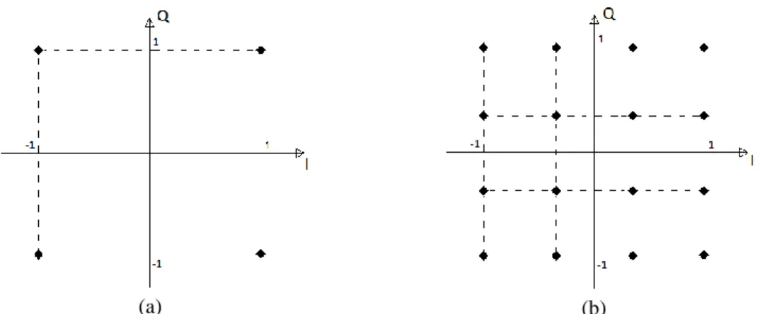
(19) 4. Theory. In the demodulator, the peak of the modulated signal can be obtained using a simple lowpass filter. In digital communication, data is first transformed to binary form, i.e. the baseband data amplitude can only take values of 0 and 1. The baseband data is first applied to a serial to parallel convertor to generate two set of data (XI and XQ) with half data rate. These two sets of data modulate two orthogonal signals having the same carrier frequency to generate In-phase (I) and Quadrature (Q) components of final modulated signal. I- and Q-signals are then added to form the final modulated signal (Figure 2-1). This is called quadrature amplitude modulation (QAM) (3).. Figure 2-1 QAM modulation scheme. The final modulated signal (RF signal) as the sum of I- and Q-components is mathematically given by: 𝑆𝑅𝐹 = 𝑋𝐼 cos(𝜔𝑡) + 𝑋𝑄 sin(𝜔𝑡). 2-5. where SRF is the RF signal, and ω is the angular frequency of the local oscillator. The simplest M-QAM modulation scheme is QAM. In QAM, XI and XQ can only take two values of -1 and 1. In total, 22 = 4 symbols can be presented in QAM, every symbol contains two bits. These symbols are shown in Figure 2-2a.. (a) (b) Figure 2-2 (a) QAM modulation symbols, (b) 16-QAM modulation symbols.
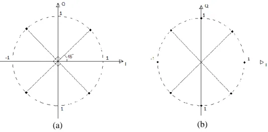
(20) Theory It is also possible to take every n bit of data as a symbol, then there are totally 2n symbols and the modulation is called 2n-QAM. In this case, each of XI and XQ components should represent n/2 bits in a symbol and take 2n/2 amplitude levels. For example, in 16-QAM modulation, there are totally 16 symbols, n is log216 = 4, i.e. every 4 bit form one symbol, XI and XQ take 22 = 4 amplitude levels. 16-QAM modulation symbols are shown in Figure 2-2b. It’s obvious now that in 2n -QAM modulation every symbol corresponds to n bits. The relation between bit rate and symbol rate is given by: 2-6. 𝑅𝑏 = 𝑛 𝑅𝑠 where Rs is symbol rate and Rb is bit rate. For QAM modulation n is 2. 2.2.2 Phase Modulation. In phase modulation techniques, the data is inserted in the phase of the carrier. This means that the phase of the carrier changes according to amplitude of the data. Considering: 𝑋𝐼 = cos(𝜑) and 𝑋𝑄 = sin(𝜑). 2-7. 𝑆𝑅𝐹 = 𝐴(𝑡) cos(𝜔𝑡 + 𝜑(𝑡)). 2-8. (2-5) can be rewritten as:. where 𝐴(𝑡) =. 𝑋𝐼2 + 𝑋𝑄2. 2-9. 𝑋𝑄 𝑋𝐼. 2-10. 𝜑(𝑡) = tan−1. In digital communication, baseband data is binary and can only take values of 0 and 1. The simplest phase modulation though is to transmit the carrier with 0ᵒ phase shift when baseband data is 0 and with 180ᵒ phase shift when the baseband data is 1. This is called binary phase shiftkeying (BPSK) (3). In order to use bandwidth and power more efficiently, higher order PSK modulation techniques are used. The baseband data is first applied to a serial to parallel convertor to generate two set of data (XI and XQ) with half data rate. These two sets modulate two orthogonal carrier signals with the same frequency to generate I- and Q-components of final modulated signal. Iand Q-signals are then added to form the final modulated signal (Figure 2-1). In QPSK modulation XI and XQ take two amplitude values -1 and 1. In total 4 symbols can be presented. Each symbol contains two bits. Therefore φ in (2-8) takes one of the values {45°,. 5.
(21) 6. Theory 135°, 225°, 315°}. Four symbols of QPSK modulation are shown in Figure 2-3a. It’s also possible to take every n bit of input data as a symbol. In this case M = 2n bits should be presented and φ(t) should take M values and the modulation technique is called M-PSK. An M-PSK modulated signal can be written as: 2𝜋(𝑖 − 1) 2-11 , 𝑖 = 1, 2, … , 𝑀 𝑀 For example considering n = 3, the modulation is 8-PSK and φ(t) takes 8 values: {0°, 45°, 𝑆𝑅𝐹 = 𝐴 cos 𝜔𝑡 +. 90°, 135°, 180°, 225°, 270°, 315°}. 8-PSK modulation symbols are shown in Figure 2-3b.. (a). (b). Figure 2-3 (a) QPSK modulation symbols, (b) 8-PSK modulation symbols. 2.2.3. Frequency Modulation. In frequency modulation techniques, the baseband data is transmitted via frequency changes of the carrier. This means that the frequency of the carrier changes in respect to amplitude of the baseband data. In case the baseband data is binary, it’s enough to define two frequencies for two possible values of data 0 and 1. This is called frequency-shift keying (FSK) (3). The simplest scheme of FSK could be just multiplying the binary data by an LO signal. Therefore a sin wave with frequency of 0 is transmitted when the baseband data is 0 and a sin wave with frequency of fLO is transmitted when the baseband data is 1.. 2.3 Transmission Line Any connection between two points that is used for transmitting an electromagnetic signal can be considered as a transmission line. Transmission lines examples are two-wire lines, coaxial lines and microstrip lines. Usually, microsrip lines are used for implementing circuits on printed circuit board (PCB). The cross section of a microstrip line on a PCB is illustrated in Figure 2-4..
(22) Theory. Figure 2-4 Cross section of a microstrip line implemented on PCB. In Figure 2-4, h is the height of the substrate (board), t is the thickness of the microstrip line, w is the width of the microstrip line and 𝜀𝑟 is the dielectric constant of the substrate. Calculating the characteristic impedance (Z0) of a microstrip line needs some complicated mathematical analysis. In order to make this easier, usually some approximations are considered. If t/h is assumed to be less than 0.005, then characteristic impedance can be calculated using w, h and εr (7). There are two different formulas for calculating Z0 depending on the value of w/h. In case w/h is less than 1, following formula can be used: 𝑍0 = where 𝑍𝑓 =. 𝑍𝑓 2𝜋 𝜀eff. ln 8. 𝑤 + 𝑤 4. 2-12. 𝜇0 /𝜀0 = 376.8 Ω and 𝜀eff. 𝜀𝑟 + 1 𝜀𝑟 − 1 = + 2 2. 1 + 12 𝑤. −1 2. + 0.04 1 −. 𝑤 . 2. 2-13. In case w/h is greater than 1, following formula can be used: 𝑍0 = 𝜀eff. 𝑍𝑓 𝑤 2 𝑤 1.393 + + 3 ln + 1.444 . 2-14. where 𝜀𝑟 + 1 𝜀𝑟 − 1 −1 2 𝜀eff = + 1 + 12 2 2 𝑤 In case w/h = 1, either of the formulas 2-12 or 2-14 can be used.. 2-15. Now consider the case that the width of the microstrip line should be calculated in order to have desired characteristic impedance. Again two different formulas are available. If w/h ≤ 2, following formula can be used: 𝑤 8𝑒 𝐴 = 𝑒 2𝐴 − 2. 2-16. where. 𝐴 = 2𝜋. 𝑍0 𝜀𝑟 + 1 𝜀𝑟 − 1 0.11 + 0.23 + 𝑍𝑓 2 𝜀𝑟 + 1 𝜀𝑟. 2-17. 7.
(23) 8. Theory. If w/h ≥ 2, following formula can be used: 𝑤 2 𝜀𝑟 − 1 0.61 = 𝐵 − 1 − ln 2𝐵 − 1 + ln(𝐵 − 1) + 0.39 − 𝜋 2𝜀𝑟 𝜀𝑟. 2-18. where 𝐵=. 𝑍𝑓 𝜋 2𝑍0 𝜀𝑟. 2-19. The question is how to know if w/h is less or greater than 2 before starting the calculations. One solution is to use (2-16) and (2-17) to calculate w/h, if w/h ≤ 2, the calculation is correct, otherwise (2-18) and (2-19) should be used. There are also some graphs available on internet and books (8), using which the approximate value of w/h can be found according to dielectric constant, thickness and desired characteristic impedance. Having the approximate value of w/h, it can be decided which of the formulas should be used to calculate the exact value of w/h. An RF circuit can be analyzed as a combination of transmission lines. A typical transmission line can be shown as Figure 2-5, where Z0 is the characteristic impedance, the upper line shows the incident wave and the lower line shows the reflected wave. The position of the load is usually considered at x = 0. Г0 is the ratio between incident and reflected waves in x = 0.. Figure 2-5 A typical transmission line. The voltage of a transmission line at any point can be considered as the sum of the incident signal voltage and the reflected signal voltage: 𝑉 𝑥 = 𝑉 +𝑒 −𝛾𝑥 + 𝑉 +Г0 𝑒 +𝛾𝑥. 2-20. The first term in (2-20) is the reflected voltage and the second term is the incident voltage. γ is the complex propagation constant which depends on the transmission line type: 𝛾 = 𝛼 + 𝑗𝛽. 2-21. If the transmission line is considered lossless, the real part of γ, i.e. 𝛼, can be neglected and so:.
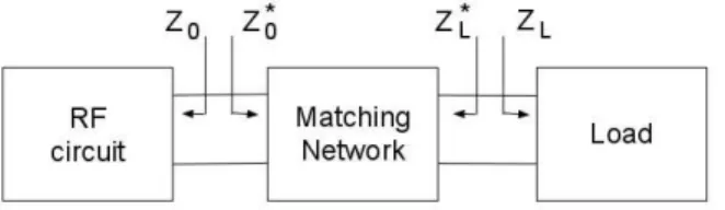
(24) Theory. 2-22. 𝛾 = 𝑗𝛽 In a similar way, the current of a transmission line at any point can be written as: 𝐼 𝑥 =. 𝑉 + −𝛾𝑥 𝑉 + 𝑒 − Г 𝑒 +𝛾𝑥 𝑍0 𝑍0 0. 2-23. According to (2-20) and (2-23), the input impedance of the transmission line at x = 0 can be written as: 𝑍(0) = 𝑍𝐿 = 𝑍0. 1 + Г0 1 − Г0. 2-24. And the reflection coefficient becomes: Г0 =. 𝑍𝐿 − 𝑍0 𝑍𝐿 + 𝑍0. 2-25. From (2-25), it can be concluded that when the transmission line is open, 𝑍𝐿 can be considered infinite and the reflection coefficient is 1. When the transmission line is short, 𝑍𝐿 is zero and the reflection coefficient is -1, and when transmission line is connected to a load with the impedance equal to its characteristic impedance (𝑍𝐿 = 𝑍0 ), reflection coefficient is zero (Table 2-1). Table 2-1 The values of reflection coefficient for some special conditions 𝑍𝐿. Г0. ∞. 1. 0. -1. 𝑍0. 0. The reflection coefficient also varies as we move along the x-axis. The reflection coefficient of a lossless transmission line at x = d can be written as: Г 𝑑 = Г0 e−2j𝛽𝑑. 2-26. The input impedance becomes: 1+Г 𝑑 1−Г 𝑑. 2-27. 𝑍𝐿 + 𝑗𝑍0 tan 𝛽𝑑 𝑍0 + 𝑗𝑍𝐿 tan 𝛽𝑑. 2-28. 𝑍𝑖𝑛 𝑑 = 𝑍0 which can be simplified as: 𝑍𝑖𝑛 𝑑 = 𝑍0. According to (2-28) any inductive or capacitive load can be created by varying parameters of. 9.
(25) 10. Theory. the transmission line, 𝑍0 , 𝑍𝐿 and d. This can be very useful in designing matching network for RF circuits. The maximum power can be transferred from a circuit to a load when the output impedance of the circuit is complex conjugate of the load impedance as shown in Figure 2-6.. Figure 2-6 Matching network. The output impedance of an RF circuit consisting of transmission lines is usually equal to the characteristic impedance of transmission lines, and the load impedance is the input impedance of the element that should be connected to the RF circuit and in general case these two impedances do not match. Matching network is a combination of inductive, resistive and capacitive elements designed to match the load to the output impedance of the circuit. In RF circuit design, matching networks are usually a combination of transmission lines and short and open stubs.. 2.4 Scattering Parameters Scattering parameter or S-parameter analysis is a powerful tool in RF circuit design (8). A simple two-port circuit as shown in Figure 2-7 can be characterized by its behavior in open and short condition. Applying short and open condition on each port of the circuit, Z, Y, h, and ABCD parameters of the network can be calculated. These parameters can be used to predict the behavior of the circuit in different conditions.. Figure 2-7 A two-port network. In case the two-port network is an RF circuit operating at high frequencies, Z, Y, h, and ABCD parameters are not so useful. It’s not easy to apply open or short condition on an RF circuit, as the circuit might become oscillating and this probably harms the device under test (DUT). Instead, matching condition is applied and the incident and reflected power waves are.
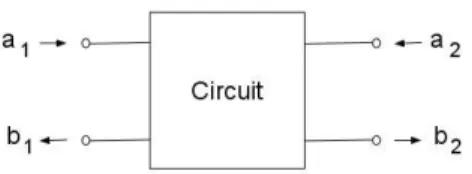
(26) Theory. studied in each port as shown in Figure 2-8 (9).. Figure 2-8 Incident and reflected power waves in a two port network. In Figure 2-8, 𝑎𝑛 is defined as incident normalized power wave and bn is defined as reflected normalized power wave as follows: 𝑎𝑛 =. 𝑏𝑛 =. 1 2 𝑍0 1 2 𝑍0. 𝑉𝑛 + 𝑍0 𝐼𝑛. 2-29. 𝑉𝑛 − 𝑍0 𝐼𝑛. 2-30. Using forward and backward travelling waves (2-29) and (2-30) can be rewritten as: 𝑉𝑛+. 𝑎𝑛 =. 𝑏𝑛 =. 𝑍0 𝑉𝑛− 𝑍0. =. 𝑍0 𝐼𝑛+. = − 𝑍0 𝐼𝑛−. 2-31. 2-32. The S-parameter matrix of a two port network such as Figure 2-8, identifies the relation between incident and reflected power waves: 𝑏1 𝑆11 𝑆12 𝑎1 = 𝑏2 𝑆21 𝑆22 𝑎2. 2-33. where, 𝑏. 𝑆11 = 𝑎1. 1. ≡ 𝑎 2 =0. 𝑏. 𝑆21 = 𝑎2. 1. ≡ 𝑎 2 =0. 𝑏. 𝑆22 = 𝑎2. 2. ≡ 𝑎 1 =0. 𝑏. 𝑆12 = 𝑎1. 2. ≡ 𝑎 1 =0. reflected power wave at port 1 incident power wave at port 1 ransmitted power wave at port 2 incident power wave at port 1 reflected power wave at port 2 incident power wave at port 2 transmitted po wer wave at port 1 incident power wave at port 2. Assuming that the characteristic impedances at input and output ports are equal, the relation between forward and backward travelling voltage waves can be written as:. 11.
(27) 12. Theory. 𝑉1− 𝑆11 𝑆12 𝑉1+ = 𝑉2− 𝑆21 𝑆22 𝑉2+. 2-34. The above equation can be extended for multiport networks as well: 𝑆11 𝑆12 . . . 𝑆1𝑛 𝑉1− . 𝑆21 . 𝑉2− . . . . = . . . . . . . . . . 𝑆𝑛𝑛 𝑉𝑛− 𝑆𝑛1. 𝑉1+ 𝑉2+ . . . 𝑉𝑛+. 2-35.
(28) An Overview on Six-Port Correlator. 3 An Overview on Six-Port Correlator Six-port technique was introduced for the first time as a measurement technique in 1970s by Engen and Hoer (9). This measurement technique is based on the fact that applying input and output signals of the DUT with different phases, would cause different signal powers at the sixport output ports (10). Many applications have been introduced for the six-port correlator since then. One of the applications proposed for the six-port correlator is signal modulation and demodulation (11). Several papers are published introducing methods to perform Q-PSK and MQAM modulation and demodulation using the six-port (1), (2), (12), (13), (14).. 3.1 Six-Port Correlator One of the possible topologies of a six-port correlator, which is used in this project work, consists of one Wilkinson power divider, and three quadrature (90°) hybrids (15). The block diagram of the six-port correlator is illustrated in Figure 3-1.. Figure 3-1 Block diagram of the six-port correlator. In Figure 3-1, Pi (i = 1, 2, . . , 6) can be defined as input, output or terminated port, depending on the application that the six-port correletor is used for. 3.1.1 Wilkinson Power Divider Wilkinson power divider is a three-port transmission line network (7). It can either be used to divide the input power from port 1 between two output ports 2 and 3, or combine the input power from ports 2 and 3 in port 1. Schematic of a Wilkinson power divider is shown in Figure 3-2.. 13.
(29) 14. An Overview on Six-Port Correlator. Figure 3-2 Schematic of a Wilkinson power divider. All three ports of the Wilkinson power divider are matched and ports 2 and 3 are isolated and lossless. The S-parameter matrix of the Wilkinson power divider is: 0 [S] = i 2 i 2 . i. 2 0 0. i. 2 0 0 . 3-1. Applying the input voltage at port 1 in Figure 3-2, and considering following condition: 𝑉1+ = 𝑉𝑖𝑛 = 𝐴 cos(𝜔𝐿𝑂 𝑡). 3-2. V1 0. 3-3. V2 V3 Vout. 3-4. V2 V3 iV1 / 2 ( A / 2 ) cos( LO t 90). 3-5. the following equation results:. So this device divides the input power between two output ports equally, with 90° phase difference with the input. 3.1.2. Quadrature (90°) Hybrid. Quadrature hybrid is a four port network with matching condition in all ports (7).. Figure 3-3 Schematic of a quadrature hybrid coupler.
(30) An Overview on Six-Port Correlator. The schematic of a quadrature hybrid is illustrated in Figure 3-3. In the quadrature hybrid shown in Figure 3-3, there is 90º phase difference between ports 2, 3 and 4. The quadrature hybrid can be used either with ports 1 and 4 as input ports and ports 2 and 3 as output ports, or with port 1 as input port and ports 2 and 3 as output ports, while port 4 is Z0 terminated. The Sparameter matrix of hybrid coupler is:. [S] =. 0 1 1 0 𝑗 0 0 𝑗. −j 2. 𝑗 0 0 𝑗 0 1 1 0. 3-6. Considering matching condition in all ports following equations can be written: 𝑉1− = 𝑉4− = 𝑉3+ = 𝑉2+ = 0 𝑉2 = 𝑉3 =. −j 2 1 2. 𝑉1 +. 1. 𝑉1 −. 2 𝑗 2. 3-7. 𝑉4. 3-8. 𝑉4. 3-9. 3.2 Signal Modulation Using Six-Port Correlator One of the applications of the six-port correlator is signal modulation. As mentioned in Section 2.4, S-parameter analysis is a powerful tool in RF circuit design. In this section signal modulation with six-port correlator is discussed based on the S-parameter matrix of the six-port correlator. Using (3-1) and (3-6) the total S-parameter matrix of the six-port correlator in Figure 3-1 can be written as (2): 0 0 −1 𝑗 0 0 1 𝑗 1 −1 1 0 0 𝑆 = 𝑗 0 0 2 𝑗 −1 1 0 0 𝑗 −1 0 0 According to (2-35), the above equation results in:. −1 𝑗 𝑗 −1 0 0 0 0 0 0 0 0. 3-10. 15.
(31) 16. An Overview on Six-Port Correlator. −𝑉3+ + 𝑗𝑉4+ − 𝑉5+ + 𝑗𝑉6+ 𝑉1− 𝑉3+ + 𝑗𝑉4+ + 𝑗𝑉5+ − 𝑉6+ 𝑉2− 𝑉3− −𝑉1+ + 𝑉2+ − = 𝑉4 𝑗𝑉1+ + 𝑗𝑉2+ 𝑉5− −𝑉1+ + 𝑉2+ − 𝑉6 𝑗𝑉1+ − 𝑉2+. 3-11. Considering following condition: 𝑉𝑛+ = Γ𝑛 𝑉𝑛− , n = 1,2,3,4,5,6. 3-12. V1 = 𝑉𝐿𝑂. 3-13. V2 = 0. 3-14. where Γ𝑛 is the reflection coefficient at the ports of the six-port correlator, (3-11) can be expanded as following:. V3 31V3 1 2V1 V3 1 2 3V1. V4 41V4 1 2 jV1 V4 1 2 j4V1 V5 51V5 1 2V1 V5 1 2 5V1 V6 61V6 1 2 jV1 V6 1 2 j6V1. V2 11V1 V3 jV4 jV5 V6 1 2 (1 2 3V1 1 2 4V1 j1 2 5V1 j1 2 6V1 ) V2 1 4 (3V1 4V1 j5V1 j6V1 ) 1 4 (3 4 j5 j6 )V1 V2 1 4 [Γ 3 Γ 4 j(Γ 5 Γ 6 )]VLO. 3-15. Now considering 𝑉𝐿𝑂 = cos(𝜔𝐿𝑂 𝑡) and comparing (3-15) and (2-4), we come to the conclusion that for signal modulation it is enough to vary reflection coefficients at ports 3, 4, 5 and 6 accordingly to the baseband data. For example, for QAM modulation considering: 𝛤3 = 𝛤4 = 𝑋𝐼. 3-16. 𝛤5 = 𝛤6 = 𝑋𝑄. 3-17. where XI is the in-phase (I) component of the baseband data and XQ is the quadrature (Q) component of the baseband data, following signal is generated at the output port:.
(32) An Overview on Six-Port Correlator. V2 1 4 X I cos(LOt ) 1 4 X Q sin(LOt ). 3-18. Comparing (3-25) and (2-5), it is obvious that the signal in (3-18) is a QAM modulated signal. The problem remained to be solved is how to vary reflection coefficients in ports 3, 4, 5 and 6 in respect to baseband data. In other words, the problem is how to convert data into reflection coefficient values. This issue will be discussed in Chapter 4.. 3.3 Signal Demodulation Using Six-Port Correlator The RF signal with M-QAM or M-PSK modulation is a combination of the baseband signal and the LO signal. The task of the demodulator is to regenerate the baseband signal from the RF signal. For signal demodulation using six-port correlator, LO signal is applied to port 1 and RF signal is applied to port 2. Considering matching condition in ports 3, 4, 5 and 6 following equations can be written: 𝑉1+ = 𝑉𝐿𝑂 = 𝐴𝐿𝑂 cos(𝜔𝐿𝑂 𝑡),. 3-19. 𝑉1− = 0. 𝑉2+ = 𝑉𝑅𝐹 = 𝐴𝑅𝐹 (𝑋𝐼 cos 𝜔𝐿𝑂 𝑡 + 𝑋𝑄 sin(𝜔𝐿𝑂 𝑡)), 𝑉3+ = 𝑉4+ = 𝑉5+ = 𝑉6+ = 0. 𝑉2− = 0. 3-20 3-21. According to S-parameter matrix of the six-port correlator (3-10 and 3-11), the signals of ports 3, 4, 5 and 6 are as following: 𝑉3 = 𝑉3− = −𝑉𝐿𝑂 + 𝑉𝑅𝐹. 3-22. 𝑉4 = 𝑉4− = 𝑗𝑉𝐿𝑂 + 𝑗𝑉𝑅𝐹. 3-23. 𝑉5 = 𝑉5− = −𝑉𝐿𝑂 + 𝑉𝑅𝐹. 3-24. 𝑉6 = 𝑉6− = 𝑗𝑉𝐿𝑂 − 𝑉𝑅𝐹. 3-25. One of the ways of regenerating baseband data from modulated signal is squaring which is used here as following: 𝑉3 = −𝐴𝐿𝑂 cos 𝜔𝐿𝑂 𝑡 + 𝐴𝑅𝐹 (𝑋𝐼 cos 𝜔𝐿𝑂 𝑡 + 𝑋𝑄 sin(𝜔𝐿𝑂 𝑡)) = cos 𝜔𝐿𝑂 𝑡. −𝐴𝐿𝑂 + 𝐴𝑅𝐹 𝑋𝐼 + sin 𝜔𝐿𝑂 𝑡 (𝐴𝑅𝐹 𝑋𝑄 ). 17.
(33) 18. An Overview on Six-Port Correlator. 𝑉32 = cos2 𝜔𝐿𝑂 𝑡 −𝐴𝐿𝑂 + 𝐴𝑅𝐹 𝑋𝐼. 2. + sin2 𝜔𝐿𝑂 𝑡 𝐴𝑅𝐹 𝑋𝑄. 2. + 2 cos 𝜔𝐿𝑂 𝑡 sin 𝜔𝐿𝑂 𝑡 −𝐴𝐿𝑂 + 𝐴𝑅𝐹 𝑋𝐼 (𝐴𝑅𝐹 𝑋𝑄 ) 𝑉4 = 𝐴𝐿𝑂 sin 𝜔𝐿𝑂 𝑡 + 𝐴𝑅𝐹 (𝑋𝐼 sin 𝜔𝐿𝑂 𝑡 + 𝑋𝑄 cos(𝜔𝐿𝑂 𝑡)) = sin 𝜔𝐿𝑂 𝑡. 𝐴𝐿𝑂 + 𝐴𝑅𝐹 𝑋𝐼 + cos 𝜔𝐿𝑂 𝑡 (𝐴𝑅𝐹 𝑋𝑄 ). 𝑉42 = sin2 𝜔𝐿𝑂 𝑡 𝐴𝐿𝑂 + 𝐴𝑅𝐹 𝑋𝐼. 2. + cos2 𝜔𝐿𝑂 𝑡 𝐴𝑅𝐹 𝑋𝑄. 2. + 2 cos 𝜔𝐿𝑂 𝑡 sin 𝜔𝐿𝑂 𝑡 𝐴𝐿𝑂 + 𝐴𝑅𝐹 𝑋𝐼 (𝐴𝑅𝐹 𝑋𝑄 ) 𝑉32 − 𝑉42 = 𝐴2𝐿𝑂 + 𝐴2𝑅𝐹 𝑋𝐼2 cos2 𝜔𝐿𝑂 𝑡 − sin2 𝜔𝐿𝑂 𝑡 + 2𝐴𝐿𝑂 𝑋𝐼 −cos2 𝜔𝐿𝑂 𝑡 − sin2 𝜔𝐿𝑂 𝑡 + 2 cos 𝜔𝐿𝑂 𝑡 sin 𝜔𝐿𝑂 𝑡 (𝐴𝑅𝐹 𝑋𝑄 ) −𝐴𝐿𝑂 + 𝐴𝑅𝐹 𝑋𝐼 −𝐴𝐿𝑂 − 𝐴𝑅𝐹 𝑋𝐼. 𝑉32 − 𝑉42 = 𝐴2𝐿𝑂 + 𝐴2𝑅𝐹 𝑋𝐼2 cos 2𝜔𝐿𝑂 𝑡 − 2𝐴𝐿𝑂 𝑋𝐼 − 2 (𝐴𝑅𝐹 𝑋𝑄 𝐴𝐿𝑂 )sin 2𝜔𝐿𝑂 𝑡. 3-26. Equation 3-26) is the sum of three signals. The in-phase component of the baseband data is generated in the second term of the equation (2𝐴𝐿𝑂 𝑋𝐼 ), which is the only part needed for demodulation application. Two other terms are extra signals which should be eliminated. Both extra terms have the angular frequency of 2𝜔𝐿𝑂 , while the central frequency of 𝑋𝐼 is zero. So there is a huge frequency difference between 𝑋𝐼 and two extra terms. This makes it easy to design a filter to eliminate the extra terms. Using a low-pass filter (LPF) for instance, the high frequency terms of (3-26) can be eliminated, and so the in-phase component of the baseband data is regenerated as following: (𝑉32 − 𝑉42 )LPF = −2𝐴𝐿𝑂 𝑋𝐼. 3-27. Performing a similar analysis for V5 and V6, quadrature component of the baseband data can be regenerated as following: (𝑉52 − 𝑉62 )LPF = −2𝐴𝐿𝑂 𝑋𝑄. 3-28. A low-pass filter eliminates two extra terms in (3-26) and all higher frequency components. Band stop filter (BSF) can be also used instead of the LPF. The BSF should be designed so that its central frequency is around 2𝜔𝐿𝑂 ..
(34) An Overview on Six-Port Correlator. 3.4 Advantages of Six-Port Correlator Six-port correlator and generally six-port technology offers several advantages which makes it a proper choice for manufacturers and researchers in many applications. Six-port correlator, as discussed, is a transmission line network which performs signal modulation or demodulation by the superposition of the phase shifted input. The main advantage of the six-port correlator is its bandwidth (16). This device can be designed to be extremely wideband, which is why it is selected for designing an UWB demodulator in this project. The wideband property of the six-port modulator also makes it suitable for receiver and particularly homodyne receiver design. The design complexity of a zero-IF receiver is less than the heterodyne receiver since by eliminating the IF-stage, there is no need to deign IF filters and image rejection parts (16), (17). However, since it is possible to design filters with transmission lines, and include them in six-port circuit, the design complexity of heterodyne receivers and even transmitters can be reduced as well. Therefore, generally the design of six-port transmitters and receivers is rather simpler compared to conventional methods. Another important property of the six-port correlator is appropriate performance in high frequency applications. It also has also low power consumption due to the fact that generally, it does not need dc-bias. Since the final design of the six-port modulator or demodulator including filters is a transmission line circuit with no dc-bias, which can easily be implemented on PCB, the fabrication price would be low. Although, the size of the board can still be a problem, as the circuit usually requires a relatively large surface. However, several researchers have been working on this problem. By designing a multi-layer layout, the size of the circuit can be reduced to an acceptably small area (10). Considering design simplicity, low power consumption and low fabrication price of the circuit, the manufacturing costs of the six-port technology are low. It can be said that six-port transmitter/receiver suggests appropriate properties for mass production. Since the design simplicity, high bandwidth, low manufacturing costs and low power consumption of the six-port technology, are desirable properties for researchers, manufacturers and product users.. 19.
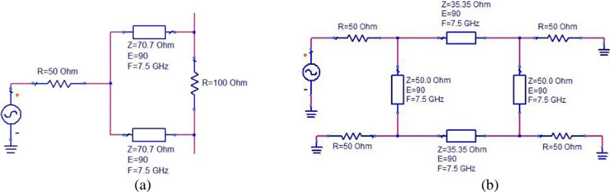
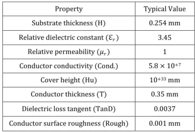
(35) 20. Six-Port Modulator/Demodulator. 4 Six-Port Modulator/Demodulator Design In this chapter, modeling and simulation of the six-port modulator and demodulator in Advanced Design System are presented. Then a typical transmitter/receiver system with six-port modulator and demodulator is modeled, simulated and analyzed.. 4.1 Six-Port QAM Modulator In order to design a six-port modulator, first the six-port correlator schematic is captured in ADS. Then, the simulation test-bench is generated by specifying the simulation type, the input signals and the termination condition. 4.1.1. Modeling Six-Port Correlator in ADS. The basic parts of a six-port correlator are power divider and quadrature hybrid. It is better to start with modeling these parts in ADS. The ADS model of Wilkinson power divider and quadrature hybrid are shown in Figure 4-1.. (a) (b) Figure 4-1 ADS model of (a) Wilkinson power divider and (b) quadrature hybrid. At first, ideal transmission line model of ADS is used to model power divider and quadrature hybrid. The system characteristic impedance (Z0) is specified as 50 Ω. According to Figure 3-2 the characteristic impedance of two transmission lines in Wilkinson power divider should be 2𝑍0 which is 70.7 Ω and their length should be λ/4 which is equivalent to an electrical length of 90º. The impedance of the resistor connecting two arms of the power divider should be 2𝑍0 , i.e. 100 Ω. According to Figure 3-3, the transmission line between ports 1 and 2, and the one between ports 3 and 4 of the quadrature hybrid, should have the characteristic impedance of 𝑍0 / 2 i.e. 35.5 Ω. The transmission line between ports 1 and 4, and the one between ports 2 and 3 of the.
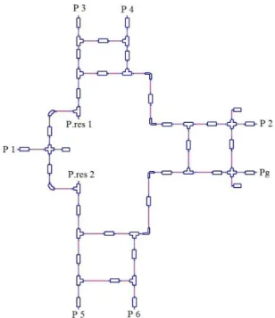
(36) Six-Port Modulator/Demodulator Design. quadrature hybrid, should have the characteristic impedance of 𝑍0 . The length of all transmission lines should be λ/4 as shown in Figure 4-1b. However, models of the power divider and quadrature hybrid using ideal transmission lines are still far from reality. The next step in the design is to make the models more realistic by replacing the ideal transmission line models in ADS with microstrip transmission lines for a given PCB substrate specification. The width and length of the transmission lines should be calculated according to the substrate specifications, for the operational frequency. The substrate selected to implement the circuit is Rogers 4350B, and it has the following specifications: Table 4-1 Specifications of Roger 4350B substrate Property. Typical Value. Substrate thickness (H). 0.254 mm. Relative dielectric constant (ℇ𝑟 ). 3.45. Relative permeability (𝜇𝑟 ). 1. Conductor conductivity (Cond.). 5.8 × 10+7. Cover height (Hu). 10+33 mm. Conductor thickness (T). 0.35 mm. Dielectric loss tangent (TanD). 0.0037. Conductor surface roughness (Rough). 0.001 mm. The width and length of a quarter-wave length transmission line at f = 7.5 GHz, with characteristic impedance of 50 Ω, on this substrate are w = 0.543811 mm, and 1λ/4 = 6.123030 mm, respectively.. Figure 4-2 ADS model of six-port correlator. 21.
(37) 22. Six-Port Modulator/Demodulator. The ADS models of power divider and quadrature hybrid should be separately tested first, then they can be combined in order to form the model of the six-port correlator as illustrated in Figure 4-2. The next step is to design the layout. The schematic should be improved further before generating the layout design. In order to increase the bandwidth, some extra transmission line might be added to the schematic. Some transmission lines should also be considered to connect the input and output ports. The resistors should be removed before creating the layout, instead some ports should be considered to connect them later. A more appropriate schematic of the sixport correlator used to generate the layout is shown in Figure 4-3. In this figure, “P.res 1” and “P.res 2” are the ports to which the 100 Ω resistance should be connected. The port “Pg” should be grounded with a 50 Ω resistance.. Figure 4-3 ADS model of the six-port correlator for layout generation. Now a layout can be created using the schematic. Then S-parameter simulation is run on the layout design in the frequency range that the circuit should be working. During this process the S-parameters of the design is calculated in several frequencies in the range. Then the model should be tested once again to see if the requirements are satisfied or not. If everything is good then ground planes, via holes and etc. are added to the layout and S-parameter simulation is run again. The S-parameter based model created after this process is an estimation of the Sparameters of the fabricated PCB..
(38) Six-Port Modulator/Demodulator Design. One of the layout designs of the six-port correlator is illustrated in Figure 4-4. However, it is not an optimum one. For example it is desired to compress the design so that it takes less area. Bandwidth is also an important issue to take care of. A variety of layouts can be designed and tested before fabrication of the PCB. Usually, optimization of the layout of the six-port correlator is an important aspect in the design. However, as the focus of this project is on the system level design, the optimization process is not presented in more detail. The layout design showed in Figure 4-4 has the bandwidth of almost 1.5 GHz, which is not appropriate for UWB applications. That is why a previously optimized layout with the bandwidth of 3 GHz is used in following steps of the project (12), (13).. Figure 4-4 Layout model of the six-port correlator in ADS. 4.1.2 Modeling the QAM Modulator in ADS As it was mentioned in Section 3.2, the baseband data in form of I- and Q-signals has to be converted into reflection coefficient values. In QAM modulation, I- and Q-components take two values therefore, a device is needed to present two values of reflection coefficient. A primary solution is to implement impedance terminations of ports 3, 4, 5 and 6 as the ideal internal resistance of an ADS switch. This switch model which is illustrated in Figure 4-5 has four ports. The impedance between ports 1 and 2 is controlled by the voltage between ports 3 and 4.. Figure 4-5 Ideal ADS model of an on-off switch. 23.
(39) 24. Six-Port Modulator/Demodulator. Grounding the ports 2 and 4 and considering the voltage of port 3 as input voltage i.e. the baseband data, the parameters of the model are selected so that the switch is open when 𝑉𝑖𝑛 = 1 and short when 𝑉𝑖𝑛 = 0. When the switch is open, ZL is ideally infinity, so the reflection coefficient at port 1 is -1, and when the switch is short, ZL is ideally zero, so the reflection coefficient at port 1 is 1: 𝑅 = 0 𝛤𝑖𝑛 = 1 𝑖𝑓 𝑉𝑖𝑛 = 0 𝑅 = ∞ 𝛤𝑖𝑛 = −1 𝑖𝑓 𝑉𝑖𝑛 = 1. 4-1. Applying baseband data to this switch, the reflection coefficient at port 1 of the switch varies accordingly to the baseband data. The six-port QAM modulator with ideal switches was modeled in ADS and, the schematic is shown in Figure 4-6.. Figure 4-6 ADS model of a simple six-port QAM modulator. According to (3-16) and (3-17) in-phase component of the baseband data should be applied simultaneously to the switches in ports 3 and 4 and quadrature component should be applied simultaneously to the switches in ports 5 and 6. Then, applying LO signal to port 1, a QAM modulated signal corresponding to (3-18) is expected to be generated at port 2 of the six-port modulator. The signal trajectory of the RF signal generated at the output port with LO frequency of 7.5 GHz, and bit rate of 500 Mbit/s is illustrated in Figure 4-7. As shown in Figure 4-7 the signal trajectory of the modulated signal corresponds to a QAM modulated signal..
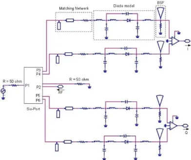
(40) Six-Port Modulator/Demodulator Design. m2. m1. Voutdn[1]. m1 time= 70.80nsec Voutdn[1]=0.660 / 43.798 m2 time= 99.00nsec Voutdn[1]=0.666 / 133.311 -0.8. -0.6. -0.4. -0.2. 0.0. 0.2. 0.4. 0.6. 0.8. m3 time= 97.70nsec Voutdn[1]=0.646 / -46.439 m4. m4 time= 80.80nsec Voutdn[1]=0.648 / -138.695. m3. time (0.0000sec to 100.0nsec). Figure 4-7 Signal trajectory of QAM modulated signal 0.6. 0.4. 4.2 Homodyne Six-Port Demodulator real(Vfund1). 0.2. 0.0. The task of the demodulator is to regenerate the baseband data from received RF signal. In -0.2. -0.4. carrier-based transmission systems, the RF signal has to be down-converted. Depending on the -0.6 0.6. receiver’s architecture, the down-conversion can be done in one or more steps. The receiver 0.4. which performs down conversion in one step is called homodyne receiver. When downimag(Vfund2). 0.2. 0.0. converting the RF signal has more than one step, the receiver is a heterodyne receiver. As shown -0.2. in Figure 4-8, the RF signal can either be first down converted to one or more intermediate -0.4. -0.6. frequencies (IF), and then to the baseband frequency using a heterodyne receiver or, be directly 0. 20. 40. 60. 80. 100. time, nsec. down-converted to the baseband frequency using a homodyne receiver.. Figure 4-8 Homodyne and heterodyne down conversion. According to (3-27) and (3-28), for signal demodulation using six-port correlator the signals in ports 3, 4, 5 and 6 should be squared first. Then the squared signal of port 3 should be subtracted from the squared signal of port 4 and the squared signal of port 5 should be subtracted from the squared signal of port 6. These signals should be then filtered. In this project diodes are used for squaring and behavioral model of operational amplifier is used for subtracting signals. A band-stop filter is used to eliminate high frequency components of the signal. The schematic of the six-port demodulator is illustrated in Figure 4-9. The components of the demodulator in Figure 4-9 are explained in following sections.. 25.
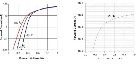
(41) 26. Six-Port Modulator/Demodulator. Figure 4-9 Schematic of the six-port correlator. 4.2.1. Modeling of Diode. In the design process it is desirable to have the models of the components as realistic as possible. In this case the element which should be modeled is the squaring diodes shown in Figure 4-9. A diode model appropriate for the circuit should be selected first. The operation frequency and speed are important elements to consider. The real model of the diode including all parasitic elements can be found in the diode datasheet. Having this information the ADS model of the diode can be prepared. The diode model HSMS-286Y from Avago Technologies is chosen for this project. The ADS model of this diode according to the diode datasheet is illustrated in Figure 4-10.. Figure 4-10 ADS model of HSMS-286Y diode. The voltage-current (V-I) characteristic of the real diode from diode datasheet and simulated V-I characteristic of the ADS model of the diode are illustrated in Figure 4-11..
(42) Six-Port Modulator/Demodulator Design. (a) (b) Figure 4-11 Voltage-current graph of (a) the real diode and (b) ADS model of the diode. The graphs in Figure 4-11 are similar, especially in the range where the voltage is below 0.2 V, which is the operational range of diode in this project. The diodes are zero biased and, used in the non-linear region, since they are used for squaring the signal. 4.2.2 Matching Network The output impedance of the six-port correlator is 50 Ω, while the input impedance of the diode is (2.477 - j36.534) Ω. In order to transfer maximum power from six-port to the diodes, a matching network should be designed. 𝑍𝑜𝑢𝑡 (𝑠𝑖𝑥 −𝑝𝑜𝑟𝑡 ) = 50 𝛺. 4-2. 𝑍𝑖𝑛 (𝑑𝑖𝑜𝑑𝑒 ) = (2.477 − j36.534) 𝛺. 4-3. and. The matching network is designed in three steps. As the real part of the diode impedance is low, the position of the load impedance in Smith chart is close to the outer circle, as shown in Figure 4-12a. It’s difficult to match such a load to the center of the Smith chart using only stubs and transmission lines. So the real part of the diode impedance is first increased using a 100 Ω resistance. The effect of the resistance is shown in Figure 4-12a as the arrow number 1. In next step, the load is rotated 112º using a transmission line so that the real part of the admittance is 1. This is shown in Figure 4-12a with the arrow number 2. Then the imaginary part of the load should be eliminated. This can be done using an open stub. The electrical length of the needed stub is calculated to be 41.8º as shown in Figure 4-12a with arrow number 3.. 27.
(43) 28. Six-Port Modulator/Demodulator. (a) (b) Figure 4-12 (a) Process of matching load and source in Smith chart, (b) Matching network. Now it’s left to calculate the real length of the transmission line and stub using their rotation angles and the substrate specifications. Considering operating frequency of 7.5 GHz, these lengths are:. 4.2.3. 𝐸𝑠𝑡𝑢𝑏 = 41.892° ⇒ 𝐿𝑠𝑡𝑢𝑏 = 2.85 𝑚𝑚. 4-4. 𝐸𝑇𝐿 = 112.154° ⇒ 𝐿𝑇𝐿 = 7.63 𝑚𝑚. 4-5. Band-Stop Filter. According to (3-26), the only high frequency component that should be eliminated from the signal before regenerating the baseband data is 2𝜔𝐿𝑂 . A quarter-wave length open stub, acts as an RF ground for the 2𝜔𝐿𝑂 component. However the same stub is an open circuit for baseband data and doesn’t affect it. In this project a microstrip radial stub is designed and used as a band stop filter to eliminate 2𝜔𝐿𝑂 component (see Figure 4-13).. Figure 4-13 Band stop filter for eliminating 2𝜔𝐿𝑂 components. The width of this stub, i.e., Wi in Figure 4-13, is the same as the width of the 50 Ω transmission line for the specified substrate. Two other parameters, the length (L) and angle.
(44) Six-Port Modulator/Demodulator Design. (Angle) are selected and optimized by performing a parameter sweep.. 4.3 Heterodyne Six-Port Demodulator In the demodulator usually some signal processing is needed in addition to frequency down conversion, in order to regenerate baseband data, and this process is more difficult for high frequency RF signals. One solution for this problem is heterodyning. In this project a heterodyne demodulator is also implemented and modeled in ADS. The frequency of the RF signal is first reduced to fIF = 900 MHz. Then the baseband data is regenerated using the IF signal. The ADS model of the heterodyne demodulator is illustrated in Figure 4-14.. Figure 4-14 Heterodyne six-port demodulator. A problem which appears in heterodyne receiver is that some extra harmonics are generated within the stages of down-conversion. The IF frequency is 900 MHz, which is down converted to baseband signal using an LO with the same frequency. By mixing IF and LO signals two frequency components are generated: 𝑓𝑏𝑏 = 𝑓𝐼𝐹 − 𝑓𝐿𝑂. 4-6. 𝑓𝑒𝑥 = 𝑓𝐼𝐹 + 𝑓𝐿𝑂 = 1.8 GHz. 4-7. where fbb is frequency of baseband signal and 𝑓𝑒𝑥 is the frequency of the extra harmonic. In order to eliminate the extra harmonic a low-pass filter with 3dB frequency of 650 MHz is. 29.
(45) 30. Six-Port Modulator/Demodulator. placed after the mixer of the IF stage. The bandwidth of baseband data is 1 GHz (-500 MHz to 500 MHz). So the baseband signal is inside the pass band of the filter, while the extra harmonic is outside of the band and therefore is rejected by LPF.. 4.4. Six-Port Transmitter-Receiver System. Now that both modulator and demodulator are modeled, they can be connected with a wireless channel in order to simulate a simple wireless transmitter-receiver system. This system is shown in Figure 4-15.. Figure 4-15 Block diagram of the six-port transmitter-receiver system. The channel is a line of sight (LOS) link, and the system has following specifications: f = 7.5 GHz Bit rate = 1 Gbit/s Modulation : QAM The ADS model of the LOS link is illustrated in Figure 4-16.. Figure 4-16 ADS model of the LOS link. The ADS schematic of the system is illustrated in Figure 4-17. The homodyne demodulator was used in this system. Two random bit generators are used to generate I- and Q-data streams. Two.
(46) Six-Port Modulator/Demodulator Design berMC1 blocks from ADS are used to compare the input and output I- and Q-data and calculate BER. The total BER is calculated using following equation: BER = BERI + BERQ – (BERI)( BERQ). 4-8. The simulation is performed for different noise temperatures and path lengths.. Figure 4-17 The ADS model of the six-port transmitter-receiver system. 4.4.1 ISI problem The bandwidth of real systems is limited. This means that real systems, including channels, behave like low-pass filters when the input frequency reaches their bandwidth. A frequency limited signal cannot be time limited. Therefore the transfer function of channel in time domain is not limited. This can make a symbol to overlap with its previous and next symbols. This is called intersymbol interference (ISI) (18). This effect can be observed in the output constellation of the demodulator as the repetition of the whole constellation pattern around each symbol. The ISI effect on a QAM signal constellation is shown in Figure 4-18.. Figure 4-18 The effect of ISI on a QAM signal constellation. Usually an equalizer unit is designed for the modulator in order to eliminate ISI effect. In this project a Gaussian band-pass filter (BPF) is used in demodulator in order to limit the bandwidth 1. Error Probability measurement using Monte Carlo Method, 2 inputs. 31.
(47) 32. Six-Port Modulator/Demodulator. of the symbols and eliminate ISI effect (see Figure 4-19).. Figure 4-19 The Gaussian BPF which is used to eliminate ISI effect. This BPF limits the bandwidth of the received signal in order to eliminate components which are created as the result of ISI. The bandwidth of BPF should be selected carefully so that it does not eliminate components of the main signal. 4.4.2. Simulation Results. In Figure 4-20a values of BER are shown while the path length varies between 1 m and 15 m and noise temperature is 300° K. The simulation is run for maximum 10000 symbol times, until the variance of BER reaches lower than 0.01. As a matter of fact, 10000 symbol times is not enough to obtain the real value of the BER, but it’s good just to have a view of how BER varies with path length. Some more accurate values of BER are shown in Table 4-2. Table 4-2 BER values BER. Noise Temperature. Distance. Simulation Time. 3.05613665e-26. 300° K. 1m. 21011 symbol times. 2.282286942808e-06. 300° K. 5m. 438157 symbol times. 4.336316e-06. 300° K. 7m. 46122 symbol times. In Figure 4-20b values of BER are shown while the noise temperature varies between 275°k to 375°k and the path length is 10 m. The simulation is run for maximum 10000 symbol times, until the variance of BER becomes lower than 0.01..
(48) 1. 0.003. 0.1. 0.0025 BER. BER. Six-Port Modulator/Demodulator Design. 0.01. 0.002 0.0015. 0.001. 0.001. 0.0001. 0.0005 1. 5 7 10 Path length (m). 15. 275. 300 325 350 Noise figure (ºK). (a) Figure 4-20 BER versus (a) path length (b) noise temperature. (b). 375. 33.
(49) 34. M-PSK and M-QAM Modulation Using Six-Port Correlator. 5 M-PSK and M-QAM Modulation Using Six-Port Correlator In previous chapters only QAM modulation using six-port correlator was discussed. In this chapter, higher order modulations are discussed and two new methods are presented for M-PSK and M-QAM modulation using six-port correlator1. As it was mentioned in Section 3.2, the baseband data should be mapped into reflection coefficients. An important issue in modulation using six-port is to choose a device to do this task. One approach is to use voltage-controlled impedance terminations as shown in Figure 5-1. This device should operate linearly in amplitude range of baseband data.. Figure 5-1 Voltage-controlled impedance termination. In Section 4.1, an ideal ADS switch model was used as the voltage-controlled impedance termination in Figure 5-1, with n = 2. The reflection coefficient of the first load was 1 the reflection coefficient of the second load was -1. The ideal ADS switch model is not a good choice though, when the modulation techniques with the order higher than QAM are needed.. 5.1 Method I : Differential Approach In this method,. I and Q components of the baseband data are first transformed into. differential mode, ( I+, I −) and (Q+, Q−), and then applied to the ports of the six-port. The idea is to represent I+ and Q+, with 3 and 5 and I − and Q−, with 4 and 6 respectively as following: 1. M-PSK modulation using six-port correlator is for the first time discussed in this projec.
(50) M-PSK and M-QAM Modulation Using Six-Port Correlator. 𝛤3 − 𝛤4 = 𝐼 𝛤5 − 𝛤6 = 𝑄. 5-1. The values that reflection coefficients take when I and Q vary are shown in Table 5-1. Table 5-1 Variation of reflection coefficient values in respect to I/Q data 𝐼>0. 𝐼<0. 𝐼=0. 𝑄>0. 𝑄<0. 𝑄=0. 𝛤3. 𝐼. 0. 0. ̶. ̶. ̶. 𝛤4. 0. −𝐼. 0. ̶. ̶. ̶. 𝛤5 ̶. ̶. ̶. 𝑄. 0. 0. 𝛤6 ̶. ̶. ̶. 0. −𝑄. 0. Now a voltage-controlled impedance termination with properties that are explained above is needed. Consider that device A is a voltage-controlled impedance termination which operated linearly in positive amplitude range of input voltage, as shown in Figure 5-2a, and device B is a similar device which operated linearly in negative amplitude range of input voltage, as shown in Figure 5-2b. Combining these two devices according to (5-1), a device is obtained that works linearly in the whole amplitude range (see Figure 5-2c).. (a). (b). (c). Figure 5-2 Combination of (a) and (b) can result in (c). On the other hand, if the inverse mode of input values is applied to device A, the input-output characteristic would be similar to device B (Figure 5-2b). Hence it is enough to design a device that has a linear function in positive amplitude range of input. Another aspect that should be considered is that according to (3-15), (𝛤3 + 𝛤4 ) and (𝛤5 + 𝛤6 ) are modulating signals at the output of the six port correlator. While here (𝛤3 − 𝛤4 ) and (𝛤5 − 𝛤6 ) should be modulating signals as mentioned in (5-1). This problem is easily solved by inverting 𝛤4 and 𝛤6 . A λ/4 transmission line is used in the design to perform this task as shown in Figure 5-3.. 35.
(51) 36. M-PSK and M-QAM Modulation Using Six-Port Correlator. Figure 5-3 Modulator designed with method I. A quarter-wave length (λ/4) transmission line performs 180º phase shift on the signal. This means that the output signal is the inverse of the input signal. In order to generate differential mode of baseband data, either a differential amplifier should be used or it should be created by the digital data source. It is also possible to think of adding some extra parts to the circuit to inverse the input signal. 5.1.1. 8-PSK Modulation Using ADS Ideal Switches. In this part a voltage-controlled impedance termination is designed with ADS ideal switches in order to perform 8-PSK modulation using six-port correlator. This device is then replaced by a real element. In 8-PSK modulation technique the phase of the carrier can take eight values, as mentioned in Section 2.2.2. Consequently, I and Q can take five amplitude levels. This means that the voltagecontrolled impedance terminations should be able to switch between five different loads. Figure 5-4a shows the amplitude levels of an 8-PSK modulated signal. But as it was explained in previous part, only negative or positive amplitude levels are applied to each part. Therefore, it is enough for each voltage-controlled impedance terminations to be able to represent half of the amplitude levels (positive or negative ones). The voltage-controlled impedance terminations for 8-PSK modulation are illustrated in Figure 5-4b..
Figure
+7
Related documents
C:\> nc –l –p [LocalPort] –e relay.bat Create a relay that sends packets from the local port [LocalPort] to a Netcat Client connected to [TargetIPaddr] on port
However, the board of the furniture company doubts that the claim of the airline regarding its punctuality is correct and asks its employees to register, during the coming month,
Abstract: In a six-port demodulator utilizing diodes for power detection, impedance mismatch at the interface between the six-port correlator and diodes generates unwanted
Within this family of mappings, the so-called binary reflected Gray code (BRGC) is of special importance since it has been proved in [46] to be the optimum mapping in the sense
Nisse berättar att han till exempel använder sin interaktiva tavla till att förbereda lektioner och prov, med hjälp av datorn kan han göra interaktiva
To re flect this complex nature of addiction, we have assembled a team with expertise that spans from molecular neuroscience, through animal models of addiction, human brain
Bristen på svenskkunskaper skapar även problem när det kommer till det administrativa, detta till trots att många entreprenörer, både svenska och franska,
Three input representations are examined: intensity values, products between intensity values, and local orientation in double angle representation2. The dimensionality of the
