UPTEC F 20023
Examensarbete 30 hp November 2020
Sputtering of High Quality Layered
MoS
2
films
Abstract
Sputtering of High Quality Layered MoS
2films
Sari Abid Al Shaybany
We have deposited bulk, monolayer and few-layers as well as large-scale 2D layered MoS2 thin films by pulsed DC magnetron sputtering
from an MoS2 target. MoS2 has gained great attention lately, together
with other layered Transition Metal Dichalcogenides (TMDCs), for its unique optical and electrical properties with thickness-dependent bandgap. MoS2 also transitions from an indirect to a direct bandgap
when thinned down to monolayer. This is intriguing in the fabrication of novel solar cells and photodetectors. Sputter-deposition has the advantage of producing large-scale, high-quality films, which is paramount for layered MoS2 to be applicable on an industrial level.
The quality in terms of crystallinity and c⊥-texture of sputtered bulk MoS2 was evaluated as a function of several deposition process
parameters: process pressure, substrate temperature and H2S-to-Ar
ratio. X-ray Diffraction (XRD) results revealed that the high substrate temperature of 700 °C together with reactive H2S process gas
improved the quality regardless of pressure. However, the quality was slightly improved further with increasing pressure up to 50 mTorr. We also found that the quality improved with increasing temperature up to 700 °C using pure Ar as the process gas. Rutherford Backscattering Spectrometry (RBS) analysis showed that with the addition of H2S the
stoichiometry of MoSx improved from MoS1.78 using pure Ar to fully
stoichiometric MoS2.01 at 40% H2S in the H2S/Ar mixture.
Cross-sectional Transmission Electron Microscopy (TEM) imaging revealed the high-quality 2D layered structure of the MoS2 films and a
maximum thickness of 5 nm of c⊥-growth MoS2 before the onset of the
undesirable c∥-growth. These results provide a solution with respect to
the ongoing challenge of obtaining high quality and good stoichiometry of sputtered TMDC films at elevated temperatures.
Formation of monolayer and few-layers MoS2 was confirmed by
Raman and Photoluminescence (PL) spectroscopy. The peak separation of the 𝐸2𝑔1 and 𝐴1𝑔 Raman-active modes for MoS2
monolayer was measured to 19.3 cm-1 on SiO
2/Si, increases
substantially in the transition to bilayer MoS2and exhibits bulk values
from four layers MoS2 and above. This result serves as a good
indicator of monolayer as well as few-layers MoS2 formation. The
monolayer film exhibits a strong photoluminescence peak at 1.88 eV owing to its direct optical bandgap, as compared to the indirect one of bilayer and thicker films. X-ray Photoelectron Spectroscopy (XPS) spectra of the monolayer MoSx film indicate successful sulfurization of
the molybdenum atoms and absence of residual sulfur. XPS also showed ideal stoichiometric MoS2.03 ± 0.03 of the monolayer film.
Furthermore, a uniform MoS2 monolayer was successfully grown on a
4" SiO2/Si wafer, demonstrating the large-scale uniformity that can be
achieved by sputter-deposition, making it highly applicable on an industrial level.
Handledare: Andreas Lindblad
Ämnesgranskare: Michelle Marie S. Villamayor Examinator: Tomas Nyberg
ISSN: 1401–5757, UPTEC F20 023 Teknisk-naturvetenskaplig fakultet UTH-enheten Besöksadress: Ångströmlaboratoriet Lägerhyddsvägen 1 Hus 4, Plan 0 Postadress: Box 536 751 21 Uppsala Telefon: 018 – 471 30 03 Telefax: 018 – 471 30 00 Hemsida: http://www.teknat.uu.se/student
Popul¨arvetenskaplig sammanfattning
P˚a daglig basis st¨oter vi p˚a objekt och tekniska komponenter runt omkring oss vars ytor belagts (deponerats) med tunna filmer av ett visst material. Detta kan g¨oras av olika syften, s˚a som deko-rativa och materialf¨orst¨arkande, eller ocks˚a f¨or smarta l¨osningar och energil¨osningar s˚a som inom utvecklingen av solceller. Tunnfilmer finns p˚a f¨onster, smartphones, CD-skivor, chipsp˚asen men, kanske viktigast av allt i v˚ar uppkopplade v¨arld, i alla mindre elektroniska komponenter - inte minst transistorn. En uppsj¨o av olika metoder f¨or deponering av tunnfilmer finns tillg¨angliga, men en-dast ett f˚atal anv¨ands i regel inom ett visst till¨ampningsomr˚ade. P˚a industriell skala v¨arderas ofta produktion av filmer med storskalig homogenitet, vilket leder till h¨ogre produktionstakt. En teknik som m¨oter just detta kriterie kallas ”sputtring”, som s˚aledes ofta g¨or sig mer l¨amplig f¨or masspro-duktion av exempelvis transistorer och solceller ¨an andra deponeringsmetoder. Sputtring opererar genom bombardering av k¨allmaterialet med h¨ogenergiska joner fr˚an ett plasma som formats genom att gasen som tillf¨orts deponeringskammaren joniserats. Detta bombardemang resulterar i att ma-terial frig¨ors fr˚an k¨allan, som slutligen l¨agger sig p˚a substratet som en tunnfilm.
Syftet med detta arbete var att unders¨oka kvalit´en hos sputtrade filmer av molybdendisulfid (MoS2)
- v˚art k¨allmaterial. MoS2 ¨ar en kristallin halvledare uppbyggd av 0.65 nm tunna lager best˚aende
av ett plan av molybdenatomer inbakade mellan tv˚a plan av svavelatomer. Dessa tre strata utg¨or ett s˚a kallat monolager och flera s˚adana monolager h˚alls samman inom materialet genom svaga van-der-Waals bindingar. Denna struktur ger upphov till enkel glidning mellan lagren. Materi-alet MoS2 utg¨or s˚aledes ett utm¨arkt torrt sm¨orjmedel och har sedan l¨ange anv¨ants inom
motor-och flygindustrin. MoS2 har f˚att extra uppm¨arksamhet p˚a senaste tiden, tillsammans med andra
material med liknande struktur och egenskaper s˚a som volframdisulfid (WS2), f¨or sina unika
elek-triska och optiska egenskaper som kan justeras genom att ¨andra p˚a filmens tjocklek - eller n¨armare best¨amt antal deponerade monolager - inom ramen f¨or n˚agra nanometer. Detta har p˚a sistone varit av stor betydelse inom tillverkningen av elektroniska komponeneter s˚a som transistorn. Bandgap f¨or halvledare anger den minsta m¨angd energi som kr¨avs f¨or att f¨ora en elektron fr˚an de h¨ogsta ockuperade tillst˚anden till de l¨agsta oockuperade tillst˚anden. Monolager av MoS2 uppvisar ett
v¨ardefullt ”direkt” bandgap, som underl¨attar ljusabsorption i exempelvis solceller.
Kvalit´en hos de sputtrade MoS2 filmerna unders¨oktes med avseende p˚a ett antal
processparame-trar; gastryck i deponeringskammaren, substratets temperatur, koncentration av H2S samt argon
gas i kammaren, och slutligen deponeringstid f¨or att precist forma ett/ett f˚atal monolager inom det intressanta intervallet f¨or vilket materialets egenskaper ¨andras med tjockleken. R¨ontgendiffraktion anv¨andes f¨or att karakt¨arisera filmerna med avseende p˚a de tre f¨orstn¨amnda parametrarna, d¨ar kvalit´en p˚a kristallstrukturen samt orienteringen av lagren evaluerades. Idealt ska lagren ligga par-allelt med substratytan. Resultaten indikerar p˚a att h¨ogsta trycket p˚a 50 mTorr, h¨ogsta temperaturen p˚a 700 °C, samt tillf¨orsel av H2S ger h¨ogst kvalit´e p˚a filmerna. F¨or att validera deponeringen av
ett/ett f˚atal monolager anv¨andes Raman-spektroskopi och spektroskopi av fotoluminiscens. Inom det f¨orstn¨amnda togs differensen mellan toppv¨arden av tv˚a av de Raman-aktiva vibrationsmoden f¨or MoS2. Resultatet ¨ar en differens som ¨ar beroende av antal deponerade monolager.
Monolager-filmen av MoS2gav, i egenskap av ett direkt bandgap, upphov till stark fotoluminiscens. Slutligen
gjordes en Ramananalys p˚a ett monolager deponerat p˚a en stor substratskiva, vilket p˚avisade ho-mogenitet ¨over stora ytor och s˚aledes industriell kompatibilitet av sputtrade MoS2filmer.
Acknowledgments
I would like to sincerely express my gratitude to my subject examiner Michelle Marie. S. Villa-mayor, Researcher at the Department of Electrical Engineering at Uppsala University, and examiner Tomas Nyberg, docent and Researcher at the same department, for their enormous support during the course of this work. It has been a true pleasure to work with both of you during the past months and your passion for the subject has really been an inspiration, and consequently affected the qual-ity of this thesis. I wish you the best in the future in your careers as well as personal lives, and hope that we keep in contact. Furthermore, I would like to thank Uwe Zimmermann, Associate Professor at Uppsala University, for his priceless help in fixing the substrate rotation mechanism of our magnetron sputtering system. I would also like to thank Lars Riekehr for providing us with TEM images, Sajid Husain for his help with Raman spectroscopy, Fredrik Johansson for his help with Photoluminescence (PL) spectroscopy, Tuan Tran for providing us with Rutherford Backscat-tering Spectrometry (RBS) data, and Rebecka Lindblad for her help with X-ray Photoelectron Spectroscopy (XPS) as well as providing us with XPS graphs. Thank you also to my supervisor Andreas Lindblad for coordinating with Fredrik and Rebecka. This work was supported by the FLAG-ERA grant LaMeS, by the Swedish Research Council VR Grant 2017-06816.
Contents
1 Introduction 1
1.1 Aim of the work . . . 3
2 Theory 4 2.1 Sputtering . . . 5
2.1.1 Basics of the Magnetron Sputtering Process . . . 5
2.1.2 Direct Current Sputtering . . . 9
2.2 Plasma . . . 10 2.3 Characterization Techniques . . . 11 2.3.1 Profilometry . . . 11 2.3.2 X-ray Diffraction . . . 11 2.3.3 Electron Microscopy . . . 13 2.3.4 Raman Spectroscopy . . . 14 2.3.5 Photoluminescence Spectroscopy . . . 15
2.3.6 Rutherford Backscattering Spectrometry . . . 15
2.3.7 X-ray Photoelectron Spectroscopy . . . 16
3 Experimental Procedures 16 3.1 Overview of the Magnetron Sputtering System . . . 16
3.2 Sample Preparation and Substrate Heating . . . 17
3.3 User Interface and Deposition Process . . . 19
3.4 Characterization . . . 20
3.4.1 Profilometry . . . 20
3.4.2 X-ray Diffraction . . . 20
3.4.3 Transmission Electron Microscopy . . . 21
3.4.4 Scanning Electron Microscopy . . . 22
3.4.5 Raman & Photoluminescence Spectroscopy . . . 23
3.4.6 Rutherford Backscattering Spectrometry . . . 23
3.4.7 X-ray Photoelectron Spectroscopy . . . 23
4 Results & Discussion 24 4.1 Influence of the Process Pressure . . . 24
4.2 Influence of the Substrate Temperature . . . 25
4.3 Influence of the H2S-to-Ar ratio . . . 27
4.4 Influence of the Substrate Type . . . 29
4.5 Maximum Thickness . . . 29
4.6 Monolayer and Few-layers . . . 31
4.6.1 Raman Spectroscopy . . . 31
4.6.2 Photoluminescence Spectroscopy . . . 34
4.6.3 Rutherford Backscattering Spectrometry . . . 34
5 Conclusions 36
List of Figures
1 (a) The mineral form of MoS2 known as molybdenite [11]. (b) The crystal
struc-ture of the most common naturally occurring 2H-MoS2 polytype, where a single
monolayer is built up by a plane of molybdenum atoms hexagonally sandwiched by planes of sulfide ions [6]. . . 3 2 Schematic illustration of the plasma-based magnetron sputtering system. . . 6 3 Illustration of ejected species from a target following the impact of a gas ion [22]. . 6 4 Illustration of magnets placed beneath the negatively biased target in magnetron
sputtering, forming a magnetic field outside the target [24]. This field confines the secondary electrons which move in spiral around the magnetic field lines. The elec-trons have a high probability of colliding with gas atoms, which then are ionized. . . 8 5 The circular MoS2 target utilized in our magnetron sputtering system, where the
race-track formation can be seen. . . 8 6 Diagram of the pulsed DC sputtering process [25]. . . 10 7 The grid represents a two-dimensional crystal lattice and the x-ray reflections from
the structure are shown. X-rays that are incident on the crystal at an angle θ produce constructive interference when the difference in distance traveled (2dsinθ ) is an integral number of the wavelength λ (Bragg’s law) [31]. . . 12 8 XRD spectra showing the characteristic peaks of 2H-MoS2 at certain scattering
an-gles, 2θ . See Section 4.2 in Results & Discussion for more information about this particular figure. . . 13 9 Illustration of the principle of Raman [33]. . . 14 10 Illustration of elastic collision in RBS between an ion and a sample atom [36], where
the backscattering angle (θ ) depends on the ion energy (E), as well as the mass of the ion (M1) and target nucleus (M2). . . 16
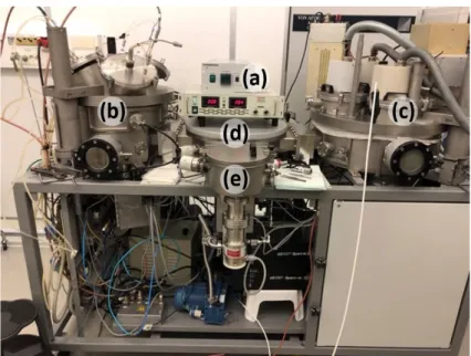
11 The complex magnetron sputtering system used in this work including (a) the heater power supply, (b) the left process chamber, (c) the right process chamber, (d) the transfer chamber and (e) the load-lock chamber. For this study, only the left process chamber was used. . . 17 12 (a) The full-size 4” diameter SiO2/Si wafer. (b) Inside view of the load-lock chamber
in which substrates were placed and from which the coated substrates were removed after deposition. . . 18 13 The heater power supply (left) and the SiC-graphite heating element on top of the
heater holder (right). . . 18 14 The user interface from which the deposition process was controlled. The buttons
represent the following: (a) power on/off controller, (b) DC power supply connected to the MoS2target, (c) transfer chamber, (d) Ar gas flow monitor and controller, (e)
left process chamber, (f) rotation controller, (g) load-lock chamber, (h) throttle valve controller, (i) left chamber pressure monitor, (j) H2S gas flow monitor and controller,
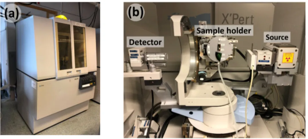
and (k) load-lock chamber pump/vent controller. . . 19 15 Phillips X’pert MRD X-ray diffractometer at ˚Angstr¨om Laboratory, Uppsala
Uni-versity. (a) Overview of the closed machine. (b) Inside view showing the source, sample holder and detector. . . 21
16 (a) Table-top magnetron sputter device used to coat the samples with gold prior to TEM imaging. (b) The FIB-SEM used to divide the samples into lamellas needed for TEM. . . 22 17 TEM system at ˚Angstr¨om Laboratory, Uppsala University, manufactured by the FEI
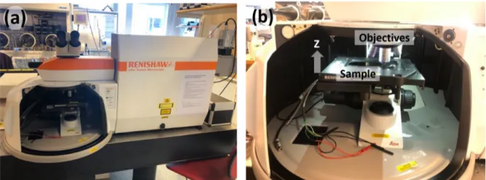
Company. The device captures a small section of the sample by transmission of electrons. The system can be seen with the safety protection doors opened and closed, respectively. . . 22 18 The SEM-Zeiss 1530. . . 22 19 (a) The Raman spectroscope at ˚Angstr¨om Laboratory, Uppsala University, provided
by the Renishaw company. (b) Inside view of the spectroscope, where the sample is seen on the sample holder underneath the ×50 magnification objective. The height of the objective (in z-direction) was adjusted prior the measurement for optimal focus. 23 20 The pressure dependence of the deposition rate of MoS2. The rate of WS2deposition
at 50 mTorr is included for comparison. . . 24 21 XRD pattern of MoS2on SiO2/Si substrates for the pressure series ranging 2.5 mTorr
to 50 mTorr, at 700 °C and using 100% H2S. The dashed vertical lines depict
refer-ence diffraction peaks for 2H-MoS2. . . 25
22 (a) FWHM values and positions of (002) peaks against process pressures, and (b) I002/(I002+I010) ratios against process pressures, at 700 °C and using 100% H2S. . . 25
23 XRD pattern of MoS2 on SiO2/Si substrates heated to temperatures ranging from
500 °C to 700 °C, under 50 mTorr and using 100% Ar. The dashed vertical lines depict reference diffraction peaks for 2H-MoS2. . . 26
24 (a) FWHM values and positions of (002) peaks against temperatures, and (b) I002/(I002+I010)
ratios against temperatures, under 50 mTorr and using 100% Ar. . . 26 25 XRD pattern of MoS2 on SiO2/Si substrates for different percentages of H2S in the
H2S/Ar process gas mixture, under 50 mTorr and at 700 °C. The dashed vertical
lines depict reference diffraction peaks for 2H-MoS2. . . 28 26 (a) FWHM values and positions of (002) peaks against % H2S, and (b) I002/(I002+I010)
ratios against % H2S in the H2S/Ar gas mixture, under 50 mTorr and at 700 °C. . . . 28
27 Top view SEM images of (a) bulk MoS2using 100% Ar, (b) bulk MoS2using 100% H2S, and (c) monolayer MoS2using 100% H2S, in the H2S/Ar process gas mixture. 29
28 XRD pattern of MoS2 grown on various substrate types, under a pressure of 50
mTorr, at 700 °C and using 100% H2S. The dashed vertical lines depict reference diffraction lines. . . 30 29 High resolution cross-sectional TEM images of bulk MoS2, under 50 mTorr, at 700
°C and using 100% H2S, after (a) 50 minutes deposition, and (b) 3 hours deposi-tion. The blue spheres represent Mo atoms, which are sandwiched between S atoms (represented by yellow spheres) and thus forming one monolayer of MoS2. . . 30
30 Raman spectra of monolayer and few-layers, as well as bulk (8 monolayers) MoS2 samples of (a) SiO2/Si substrates and (b) sapphire substrates. The dashed lines are
placed at the bulk values. . . 31 31 (a) Change in the E2g1 and A1gRaman modes with thickness and (b) their difference,
for MoS2films on SiO2/Si substrates. . . 32
32 (a) Change in the E2g1 and A1gRaman modes with thickness and (b) their difference,
33 (a) Raman mapping of the peak separation, A1g− E2g1 , of monolayer MoS2grown on
a full-size 4” SiO2/Si wafer. The black dots mark the spots of where the data were
recorded to plot the map. (b) A1g− E2g1 as a function of number of monolayers. The
shaded rectangle depicts the range of peak separation values across the wafer-scale MoS2monolayer. . . 33
34 PL spectra of monolayer and bilayer MoS2 grown on SiO2/Si substrates. The inset
shows a magnified, red-shifted ”A” peak of the bilayer film, which is the signature PL peak for G6-TMDCs such as MoS2. . . 34
35 XPS spectra of (a) molybdenum 3d and (b) sulfur 2p core levels, for monolayer MoSx grown on the conductive Si substrate, under 50 mTorr, at 700 °C and using
Definitions and Abbreviations
Definitions
2D material Material with a very thin layered structure
as-sputtered Films deposited in one step without sequential annealing in a sulfurized H2S atmosphere
c⊥-growth Layered film growth with the 2D layers parallel to the substrate surface ck-growth Layered film growth with the 2D layers perpendicular to the substrate
surface
chalcogen An element in group 16 of the periodic table (oxygen family) chamber The vacuum space in which the deposition process takes place elastic scattering Scattering of a particle upon interaction with other particles where its
wavelength is conserved though its direction of propagation is altered H2S-annealing Heating of a film at elevated temperature in H2S gas
metastable (e.g. of an ion or neutral atom) existing in an excited state with a relatively long lifetime
monochromatic Single wavelength electromagnetic radiation
monolayer The three strongly bound strata of atomic planes in TMDC materials sample The thin film coated substrate after the deposition process
sputtering Deposition technique where the target material is ejected and condensed on the substrate, following high-energetic ion bombardment of the target reactive sputtering Sputtering of a target in the presence of a reactive gas (e.g. H2S)
substrate The undeposited material
Abbreviations
General
AC Alternating Current
DC Direct Current
FWHM Full Width at Half Maximum
ML Monolayer
RF Radio Frequency
TMDC Transition Metal Dichalcogenide
Chemical symbols
Al2O3 Sapphire
Ar Argon
H2S Hydrogen sulfide
MoS2 Molybdenum disulfide
S Sulfur
Se Selenium
SiO2/Si Silicon dioxide deposited Si substrate
WS2 Tungsten disulfide
Deposition & characterization techniques
CVD Chemical Vapor Deposition
PL Photoluminescence
PVD Physical Vapor Deposition
RBS Rutherford Backscattering Spectrometry
SEM Scanning Electron Microscopy
TEM Transmission Electron Microscopy
XPS X-ray Photoelectron Spectroscopy
1
Introduction
Thin film deposition manufacturing processes are at the heart of today’s semiconductor industries, on solar panels, CDs, disk drives, electronics and optical devices [1]. The purposes of the thin film coating range from purely aesthetic ones, to material strengthening, smart material solutions and energy applications like solar cell development. Although a wide range of deposition techniques are at our disposal for producing desired nanomaterials within many of the existing applications of MoS2, only one or two specific methods are customarily employed in each application area. The
various techniques all come with their advantages and difficulties, and the choice of method comes down to technical criteria related to the application of the product. M. Samadi et al. [2] points out the four most important criteria for utilizing a production technique in terms of application; lateral size and thickness (average number of monolayers) as well as throughput and crystalline qualities [2]. Other important considerations may include cost, source material availability and compositional control [3]. In this work depositions were carried out using a sputtering process for producing large-scale uniform thin MoS2films with good crystalline quality, orientation of the 2D
layered structure and stoichiometry. Sputtering is more suitable for mass production compared to other existing deposition techniques [4]. It is the process used to deposit on precision devices, e.g. transistors, photodetectors and solar cells [2].
Although a whole range of solid materials are fit for sputtering (metals, semiconductors or insu-lators), deposition of nanosheet layered 2D materials, such as graphene, boron nitride and semi-conducting transition metal dichalcogenides (TMDCs) (including MoS2) have gained worldwide
attention in the last decades due to their unique properties. Graphene (discovered in 2004) comes with a lot of advantages in terms of its exceptional mechanical, electronic, optical and transport properties. However, this material lacks a bandgap, making it difficult to be integrated into elec-tronic applications. The zero-bandgap implies that graphene transistors cannot have the two con-ventional on and off states, cannot be totally switched off and has more leakage of energy as well as produces more heat. Although it is possible to use graphene for nano-electronic applications by generating a finite bandgap, such solution adds another level of complexity and even degrades material properties. For these reasons, research has been focused on semiconducting 2D materials with similar structure and characteristics that can be thinned down to a few thin layers and which exhibits strong in-plane bonds while having weak interplane interactions [5]. Among these 2D ma-terials, the semiconducting TMDCs have gained interest in recent years. Monolayer TMDCs are thin semiconductors of the type MX2 which means that they consist of transition metal atoms, M
(e.g. Mo or W), and chalcogen atoms, X (e.g. S or Se). Unlike graphene which has all the atoms in the same plane, each monolayer of a TMDC material consists of one plane of M atoms sandwiched between two planes of X atoms [6]. Among the most remarkable characteristics of TMDCs is their different properties for monolayer and few-layers ultra-thin (<10nm) films from their bulk coun-terparts, due to the quantum confinement effects [7]. One spectacular property of TMDCs is their thickness-dependent optical/electronic bandgap that increase with the film thicknesses [6]. This makes it possible to tune the optical and electrical properties of these materials by adjusting the number of monolayers. TMDCs also shift from an indirect bandgap to a direct one with decreasing
number of monolayers [4]. In addition, TMDCs generally have a rather high carrier mobility (>100 cm2V-1s-1) [2]. These properties of TMDCs has made them great alternatives to the zero-bandgap graphene recently, offering better solutions for various (opto)electronic devices and within various applications. TMDCs are promising for futuristic (opto)electronic devices, as well as for appli-cations in field-effect-transistors (FETs), photodetectors, integrated circuits, memory devices, and many other devices. The extremely low on/off ratio of pristine graphene because of its absence of a bandgap makes TMDCs the natural choice in various applications [5, 6, 2]. However, despite the highly desirable properties of TMDCs it remains a major difficulty to achieve tunable bandgaps for 2D TMDC materials for (opto)electronic applications [7].
G6-TMDCs (Group 6 TMDCs) based on molybdenum, tungsten, sulfur and selenium have gained special interest recently in (opto)electronics, sensors, energy storage and catalysis applications [2]. This study focuses specifically on sputter-deposition of molybdenum disulfide (MoS2). MoS2is an
inorganic, silvery black compound composed of molybdenum and sulfur. It is most often found in nature as a crystalline mineral and referred to as molybdenite (Fig. 1.a). Among all TMDCs, MoS2
exhibits superior optoelectronic and catalytic properties compared to the conventional semiconduc-tors [6]. It is expected to be utilized in futuristic nano-scale devices since layered n-type MoS2has
a relatively high electron mobility (~700 cm2V-1s-1), even in thin films and within the mentioned, wide bandgaps. The high mobility enables a high on/off current ratio (~108) for MOSFET’s [4]. Being part of the TMDC family, monolayer 2H-MoS2 is composed of a plane of molybdenum
atoms sandwiched by planes of sulfide ions (Fig. 1.b). The 2H phase of MoS2 is the
thermody-namically favored polytype found in nature and refers to the stacking order of the unit cell [8]. The letter ”H” indicates the hexagonal crystal lattice and the preceding digit ”2” refers to the two molecules in the unit cell. The 2H phase polytype is the one developed in this study. The three atomically thin strata form the 6.5 ˚A thick monolayer of MoS2. These monolayers are the
build-ing blocks of bulk MoS2. Bulk MoS2 is composed of stacks of monolayers with strong covalent intralayer bonding, kept together by relatively weak interlayer van-der-Waals interactions [2]. The van-der-Waals type bonding between sulfur-occupied lattice planes allow for easy sliding of crystal planes, which makes MoS2an excellent dry lubricant together with other G6-TMDCs such as WS2 [9]. MoS2has for these reasons been long-used in fields of aerospace and high vacuum technology.
As with other TMDCs, the number of monolayer MoS2 can be adjusted in order to tune its
opti-cal/electrical properties due to the thickness-dependent optical/electronic bandgap. For MoS2, the optical bandgap ranges from an indirect 1.3 eV as a bulk, to the favorable direct bandgap of 1.9 eV (the electronic bandgap is 2.5 eV) achievable by thinning down the MoS2 to monolayer [2]. This
remarkable transition from indirect to direct bandgap of MoS2was first reported by K. F. Mak [10] in 2010, making MoS2 monolayer the first atomically thin material that is an effective emitter of
light. This is intriguing for fabrication of novel light emitting diodes, solar cells and photodetec-tors. MoS2 has in fact become a more frequent material in the fabrication of light emitted diodes (LEDs) and as a photovoltaic absorber material in thin film solar cells [9].
MoS2, or TMDCs in general, have some clear advantages in comparison to the 3D-material silicon (Si) as well. These advantages are especially evident when it comes to creating microchips for miniaturization. Electrons can move around as quickly in an extremely thin 6.5 ˚A sheet of MoS2
as in a 20 ˚A thick sheet of Si. Since it is not possible to fabricate a layer of silicon to the degree 2
Figure 1. (a) The mineral form of MoS2 known as molybdenite [11]. (b) The crystal structure of
the most common naturally occurring 2H-MoS2polytype, where a single monolayer is built up by
a plane of molybdenum atoms hexagonally sandwiched by planes of sulfide ions [6].
of thinness as MoS2, futuristic chips involving MoS2are expected to become smaller than
state-of-the-arts Si chips [6]. (Opto)electronics has been the most active area of applications of MoS2over
the last decade as silicon-based semiconductors had reached their fundamental performance limits and the demand for faster devices with lower power consumption is much greater. MoS2 has, for
instance, become a great alternative to Si for transistor manufacturing [2].
1.1
Aim of the work
In this work, we deposit MoS2thin films by pulsed direct current (DC) magnetron sputtering from
an MoS2 target. The purpose of the work is to expand the process parameters with respect to
previous works [12, 13, 14], in order to draw conclusions and increase the level of understanding regarding MoS2 film growth during sputtering. The process parameters were modified to obtain high-quality 2D layered MoS2. In previous studies, the quality of as-sputtered MoS2 films at low
temperatures was enhanced by post-deposition H2S-annealing at elevated temperature to
compen-sate for the relatively deficient sulfur atoms in the as-sputtered films [12, 13, 14]. In this work, high-quality MoS2 films were achieved in a one-step process with an elevated substrate
tempera-ture of 700 °C together with sulfur as a source material and without post-deposition H2S-annealing.
The hope is that the additional sulfur from the compound MoS2target (instead of a Mo target) as well as from reactive H2S gas help to eliminate sulfur vacancies normally induced by sputtering of
2D TMDC (including MoS2) films at elevated temperature [15]. The repair of sulfur vacancies
im-proves crystallinity as well as reduces the probability of an undesirable transition of the film growth from a preferred structure where the layers are parallel to the substrate (c⊥-growth) to an
undesir-able structure where the layers are perpendicular to the substrate (ck-growth). Moreover, the sulfur vacancies (and other crystal defect) create energy levels close to the conduction band resulting in reduced carrier mobilities [16], which impairs device performance. Such structural defects must therefore be avoided or repaired in order to for instance realize high mobility 2D MoS2transistors.
The work is divided into two main parts. In the first part, the quality in terms of crystallinity and c⊥
-texture of reactively sputtered bulk MoS2films onto SiO2/Si substrates were evaluated as a function
of process pressure (2.5-50 mTorr) and relative amount of H2S (0-100%) in the H2S/Ar process gas
mixture. The influence of the substrate temperature (500-700 °C) on the quality at 100% Ar (0% H2S) was evaluated as well. The stoichiometry of MoSx was obtained for the films in the H2
S-to-Ar ratio series. Besides growing films on SiO2/Si, films were also grown on unoxidized Si and
sapphire substrates to obtain the substrate dependence on crystalline quality. The maximum thick-ness of c⊥-oriented growth of MoS2, before the onset of ck-growth, was also investigated. The
films were characterized by X-ray Diffraction (XRD), Transmission Electron Microscopy (TEM) and Rutherford Backscattering Spectrometry (RBS).
In the second part, controlled high-quality monolayer and few-layers MoS2 films were deposited
and characterized by Raman and photoluminescence (PL) spectroscopy. A Raman analysis of a full-size 4” SiO2/Si wafer coated with monolayer MoS2was conducted in order to demonstrate the
advantage of large-scale uniformity that is characteristic of sputtering [4]. This demonstration was carried out in the light of the ongoing challenge of developing reliable and high-throughput deposi-tion techniques on large area substrates. This is paramount for layered MoS2to be applicable on an
industrial level as a candidate channel material for (opto)electronic devices [17]. The stoichiometry of the monolayer film was analyzed by both RBS and X-ray Photoelectron Spectroscopy (XPS), and the chemical states of the monolayer was analyzed by XPS.
The remainder of this thesis is organized as follows: in Section 2, the theory related to the experi-ments is given, including an explanation and discussion of the magnetron sputtering technique put into context with other deposition methods for MoS2. The section ends with a theoretical
introduc-tion to the relevant characterizaintroduc-tion techniques. Secintroduc-tion 3 provides informaintroduc-tion of the magnetron sputtering system and the characterization tools utilized, as well as a description of the experimental procedures related to the sample preparation, deposition process and characterization, respectively. Section 4 provides the results discussed thoroughly and compared to the literature. Finally, Section 5 concludes the results.
2
Theory
Thin films deposition is the technology of applying a very thin film of a material onto a substrate surface to be coated, or onto previously deposited coating to form layers. The thickness of such a film can vary, but is typically in the range of around 100 micrometers down to a few ˚angstr¨oms [1], i.e. the thickness of a relatively small number of atoms, as in the case of monolayer and few-layers MoS2.
The field of thin film deposition is typically categorized into two broader divisions of the field -Chemical Vapor Deposition (CVD) and Physical Vapor Deposition (PVD). The former is a broad umbrella term referring to a wide range of deposition techniques where a volatile fluid precursor produces a chemical change on a surface leaving a chemically deposited coating on the substrate.
One common application of CVD is in the production of the highest-purity, highest-performance solid materials in the modern industry of semiconductors [1].
PVD systems, also a collective set of different deposition techniques (including sputter-deposition), essentially operate by releasing (vaporizing) material from a source - the target - which is then de-posited and condensed on a substrate to form a thin film layer, using electromechanical, mechanical, electromechanical or thermodynamic processes. Among the general advantages of PVD coatings over CVD coatings are their much greater durability, i.e. the coatings are hardier with better resis-tance to corrosion, and hence PVD is more applicable in the pursuit of long-lasting coatings [18]. PVD techniques are also more suited for substrates that cannot tolerate relatively high tempera-tures, since CVD processes (necessarily) run at much higher temperatures than PVD processes. Thus, PVD processes have a wider range of materials available for deposition. Moreover, unlike in CVD, PVD processes do not require the use of specialized precursor materials, which consti-tutes another advantage over CVDs. These precursors (and by-products) may be toxic, pyrophoric, or corrosive, possibly causing issues with material handling and storage. PVD processes are thus advantageous also in terms of safety [3]. However, in this study we used poisonous H2S gas to
increase the sulfur content on the film.
PVD (and CVD) techniques differ in the way they generate and deposit the material. Nowadays, the two commonly used PVD techniques are thermal evaporation and sputtering. In the former, the source material is vaporized by heating in vacuum, resulting in a gas phase of the material which diffuse through the vacuum to the substrate [19]. Sputtering, on the other hand, uses different methods to generate and deposit the source material (the target), described in Section 2.1, followed by a brief description of plasma in Section 2.2 and the theory behind the characterization techniques utilized in Section 2.3.
2.1
Sputtering
This section provides a description of the basic principles of pulsed DC magnetron sputtering. This is the deposition technique utilized in this work, and the one producing the highest scalability among all PVD technique [20]. Sputtering processes in general do not require elevated temper-atures which enables the use of virtually any vacuum compatible substrate [21]. The literature suggests that sputtering does not require as high a substrate temperature as other deposition tech-niques such as CVDs (frequently used to deposit layered MoS2) to achieve the same, high-quality
results. In CVD processes, formation of layered MoS2 requires a temperature of approximately
800 °C. In contrast, it is considered that layered MoS2 films can be formed by sputtering at such
a low temperature as 300 °C [4]. However, in this study, the high substrate temperatures (500-700 °C) were necessary in order to deposit high-quality c⊥-growth MoS2.
2.1.1 Basics of the Magnetron Sputtering Process
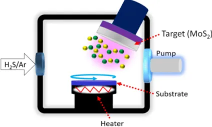
Magnetron sputtering is a PVD technique that creates vapor from a negatively charged solid surface (the target) by the bombardment of highly energetic ions from a plasma (see Fig.2). This causes a sequence of collisions in the target (Fig. 3), resulting in material from the surface of the target
Figure 2. Schematic illustration of the plasma-based magnetron sputtering system.
being ejected provided that the energy of the particles are greater than the surface binding energy. An incident ion sputters off atoms after a collision cascade and reflects neutrals and/or ions. It also leads to emission of secondary electrons and photons. The ejected material traverse the vacuum chamber and finally condense onto the substrate surface as well as all over the inner surfaces of the chamber exposed to the ejected material as a thin film coating. The plasma-based magnetron sputtering technique is often times the sputtering technique referred to on a commercial level.
Figure 3. Illustration of ejected species from a target following the impact of a gas ion [22]. The target as well as the substrate are placed facing each other inside a closely sealed vacuum chamber (Fig. 2). The process chamber is evacuated by a vacuum pump to a low base pressure in order to remove air before gases, e.g. H2S and Ar used in this study, are introduced into the system.
The electrically neutral gas atoms become ionized by the negatively biased target and a grounded surface inside the process chamber. With the right conditions, a plasma is attained consisting of excited atoms, positive gas ions, free electrons, radicals etc. (more details on plasma found in Sec-tion 2.2). The plasma is confined near the target by the magnetic field from the magnets placed behind the target. The secondary electrons ejected by the positively charged ions upon interaction with the negatively biased target (Fig. 3) are crucial to sustain this plasma. The ions of the plasma accelerate towards the target, vaporizing it, and finally the vaporized target materials settle towards the substrate. In our case, the substrate was grounded.
The process pressure inside the chamber, typically ranging from 0.5 mTorr to 100 mTorr [23], is controlled by changing the supply of the process gas by its mass flow controller and/or by regulat-ing a valve placed between the chamber and the vacuum system connected to the chamber. Most often, the pressure is set in the range of one to some tens of mTorr [21]. In order to control the amount of deposited material arriving the substrate, the sputtered material traversing towards the substrate is shielded by a shutter. That way, the substrate is only exposed to the deposited mate-rial when the shutter is open, i.e. during the desired time of deposition. Furthermore, a rotating substrate holder is most times used to obtain uniformity of the deposited material throughout the substrate. During the bombardment of the particles towards the target surface, most of the energy carried by the particles is lost in form of heat. Due to this heating phenomenon, targets are typically water cooled to prevent it from melting as well as protect the magnets from Joule heating.
As mentioned earlier, sputtering processes require much lower temperature than CVD processes to achieve the same high-quality MoS2films. This can be explained by the fact that the migration
of atoms during sputtering processes is enhanced by the kinetic energy induced by the ion bom-bardment, in addition to thermal energy. In comparison, thermal energy is the only cause of atom migration during CVD processes [4].
Magnetron sputtering, commonly powered by DC or RF power supply, achieve higher deposition rates compared to other sputtering techniques [2]. The technique makes use of the fact that the velocity and behavior of the charged ions can be regulated by the strong magnetic fields in the close proximity of the target, introduced by the magnets placed behind the negatively charged tar-get (Fig. 4). This magnetic field traps the secondary electrons right above the tartar-get. The electrons are then spiraled around the lines of the magnetic field as a consequence of the Lorentz force, thus increasing their path length which facilitates ionizing collisions with gas atoms in the vicinity of the target. The trapping of secondary electrons largely increases the ionization efficiency leading to increase in the deposition rate. A high-density plasma can therefore be sustained at even lower gas pressures (a few mTorr) and target potential (few hundred volts) [21].
One serious disadvantage with magnetron sputtering as compared to other PVD methods is the relatively low utilization of the target material due to the inhomogeneous erosion profile. This is a consequence of the fact that material erodes more efficiently where the magnetic field is strongest parallel to the surface of the target. The ejected atoms follow a typical line-of-sight cosine distri-bution from the face of the target. As the erosion track (or race track) becomes more pronounced (Fig. 5), the sputtering rate drops due to increased scattering of the target material at directions other than to the substrate [21]. Though it is possible to use rotating magnets or alternative design of the magnetic field to overcome this issue of low target material utilization, the sputtering system used in this study has stationary magnets.
The low directionality of magnetron sputtering is solved in other sputtering techniques. A com-petitor to magnetron sputtering is Ion Beam Sputtering (IBS). It is a technique in which an ion beam is focused on the target, whereby material is sputtered off onto the substrate. The process is characterized by its monoenergetic and highly collimated nature since the ions possess equal energy and directionality. This accounts for some of the great advantages of IBS over magnetron sputtering, including better uniformity, lower impurity levels, higher film quality and much better
Figure 4. Illustration of magnets placed beneath the negatively biased target in magnetron sputter-ing, forming a magnetic field outside the target [24]. This field confines the secondary electrons which move in spiral around the magnetic field lines. The electrons have a high probability of colliding with gas atoms, which then are ionized.
Figure 5. The circular MoS2 target utilized in our magnetron sputtering system, where the
race-track formation can be seen.
directionality, i.e. sputtered off material is highly controlled by means of regulating the current of ion beam during the deposition process. However, IBS comes with some disadvantages compared to magnetron sputtering, including lower deposition rates (1-2 ˚A/s) and lower scalability (leading to lower throughput) [20]. The low deposition rates of IBS is because of its low ionization efficiency of the secondary electrons, which results in a relatively low generation of ions.
Several growth parameters can influence the quality and properties of the sputtered MoS2 film.
These include the quality of the target material, the power density on the target, the gas flow rate, the substrate rotation speed, the substrate-target distance, and the supplied power from DC or RF [2]. In this work, the process parameters were limited to the few mentioned in the introduction:
pressure under which the deposition was carried out, temperature to which the substrates were heated prior to and during deposition, H2S-to-Ar ratio in the sputtering atmosphere, and finally
the sputtering duration which relates to the thickness of the film which determine the properties of TMDC films as discussed in the introduction. The substrate-dependent quality of MoS2 films has
also been reported in the literature [2] and was also investigated in this work.
Besides the mentioned parameters, the literature suggests enhanced quality of sputtered films with post-deposition H2S-annealing [13]. J. Shimizu et al. [13] found that the H2S-annealed film
re-sulted in better quality than the as-sputtered MoS2 film at low 360 °C substrate temperature. The
enhanced quality from H2S-annealing can be explained in terms of the better repair of sulfur
va-cancies, induced by the energetic particle bombardment during the sputtering process [15]. As mentioned in the introduction, a sequential H2S-annealing step was not performed for the purpose
of achieving high-quality MoS2 films in this work. Instead, high-quality films were achieved at
elevated substrate temperature of 700 °C with additional sulfur from H2S during sputtering.
The film quality may also be influenced by the state of the MoS2 target utilized. This is because
chalcogen atoms (such as sulfur atoms) depart at a higher rate than metal atoms (such as molybde-num atoms) from the surface of a new TMDC target upon sputtering. The reason for this is (a) that the mass of a sulfur atom is well-matched to incident Ar ions resulting in maximum momentum transfer and (b) because of the difference in vapor pressure between chalcogens and metals [15]. The effect of the target condition on the film quality has however not been confirmed in this study.
2.1.2 Direct Current Sputtering
Direct Current (DC) sputtering is the most basic, inexpensive sputtering type for metal/semiconductor PVD. It is advantageous in mainly two regards - it is easy to control and has low cost for deposition of metals and semiconductors [23]. As mentioned, this work uses pulsed DC sputtering of semi-conducting MoS2. The primary advantage of pulsed DC sputtering as compared to conventional
DC sputtering is the reduction or elimination of arc formation. Arcing is one of the most challeng-ing issues in PVD of thin films. It occurs whenever the target material, such as MoS2, takes on a
charge. This ultimately causes defects in the quality of the deposited film, and may also damage the DC power system. Pulsed DC sputtering works by applying the negative pulsed DC electrical current to the target material (see Fig. 6 for the exact process). This is in contrast to conventional DC Sputtering, where a constant negative voltage is applied to the target. The reduction, or elimi-nation, of arcs is achieved by pulsing the DC voltage in the range of 10 to 350 kHz with duty cycles in the 50-90 % range. Sputtering only takes place during the “on time” of the cycle, i.e. when the negative pulse is being applied [25].
Although, the issue of charge buildups can be solved by pulsed DC for metals and semiconductors, DC sputtering is not fit for insulating target materials. This is because of the lack of current running through the highly resistive insulator, which annihilates the plasma and therefore terminates the sputtering process. Extremely high voltages would be required to run a sufficient current through the insulator. Practically, insulators and otherwise highly resistive materials (above 106Ω · cm) are not applicable for DC sputtering [26]. Fortunately, these kinds of materials fall outside the scope
Figure 6. Diagram of the pulsed DC sputtering process [25].
for this study and pulsed DC sputtering may hence be utilized in the deposition of semiconducting MoS2. Otherwise, sputtering of insulators is achieved using one the more complicated technologies
available - one of which known as Radio Frequency Sputtering (RF). As opposed to DC sputtering, RF sputtering uses a periodic AC potential at radio frequencies, where the target and substrate pe-riodically behave as anodes and cathodes. The sputtering process takes place during the negative half-cycle when ions are attracted towards the target. Since G6-TMDCs are semiconductors, DC, RF and pulsed DC sputtering can all be used for their deposition [2].
2.2
Plasma
Plasma occurs naturally in the universe. Almost all the visible matter in the universe exists in the plasma state. It is occurring predominantly in the sun and other stars, as well as in interplanetary and interstellar space. Auroras, lightning and the ionosphere surrounding the earth are other natural occurrences of plasma. Besides the natural occurrence of plasma, it is also created artificially in various industries and for various applications other than for coating purposes. It is the key compo-nent to plasma TVs, neon and fluorescent lamps, and many other devices. Plasma is referred to as the fourth fundamental state of matter, as being the fourth step in the transformation of matter when subjected to an increased temperature making the atoms more energetic. Plasma is distinct from the preceding solid, liquid and gaseous states. It typically consists of roughly an equal number of positively charged ions and negatively charged free electrons, and is produced when the atoms in a gas become ionized [27].
As established, magnetron sputtering is a plasma-assisted technique that creates a vapor from the target through bombardment with gaseous ions from the plasma. The electrically neutral gas atoms 10
become excited by the electric field induced by the negatively charged target and, in our case, the grounded target shield. The atoms gets excited to metastable states or gets ionized. The light observable from plasma in the chamber results from photons emitted when the electrons in the excited ions return to their equilibrium states. Besides these excited atoms, the plasma consists of gas ions, free electrons, radicals, etc. These charged particles of the plasma makes it electrically conductive. Plasma can therefore be controlled by the electromagnetic field from the magnets behind the target. This makes it possible to confine the plasma close to the target.
2.3
Characterization Techniques
The theoretical background of the techniques utilized to characterize the films are given in this section: profilometry, XRD, TEM, SEM, Raman spectroscopy, PL spectroscopy, RBS and XPS. 2.3.1 Profilometry
A profilometer is a measuring technique used to obtain topographical data from the sample sur-face, in order to quantify its roughness, morphology and step heights. In this study, film thickness was measured from a step separating the MoS2coated and uncoated area of a dummy sample (see
Section 3.4.1). Profilometers include a detector and a sample stage. The detector determines the location of points on the sample, while the sample stage is where the sample is put. Either the detector moves, sample stage moves or both parts move to allow for the desired measurement [28]. Profilometers are either stylus-based or optics-based. A stylus profilometer uses a very light stylus that is in physical contact with the surface of the sample, while slowly moving along a set direction and follows the surface topography acquiring the surface height. It is this type of profilometer that was used in the film thickness measurements. Optical profilometers, on the other hand, use light instead of a physical stylus. The fundamental task of optical profilometry is directing the light in a way that makes it possible to detect the surface in three dimensions [28].
2.3.2 X-ray Diffraction
X-ray Diffraction (XRD) is a technique that is often utilized to assess the quality of G6-TMDC nanomaterials [2]. In particular, it is used to obtain information about the crystalline structures, atomic spacings, crystalline phases and preferred crystal orientations of G6-TMDCs [29]. Since bulk polytypes of G6-TMDCs have well documented XRD patterns, XRD can be used to distin-guish between the hexagonal (2H) and rhombohedral (3R) polytypes, and to determine the phase composition of their samples. The rhombohedral polytype is a subset of the G6-TMDC hexagonal crystal family [2]. However, the scope of this study focused only on the 2H-MoS2polytype.
XRD is based on constructive interference of monochromatic x-rays and a crystalline sample (such as a multi-layered MoS2film). The x-rays are generated by an x-ray tube that is filtered to produce
monochromatic radiation, typically within the range of 0.5 ˚A to 2.5 ˚A. The rays are then collimated and finally directed towards the sample. The x-rays then interact with the electrons of the sample atoms. As the photons of the incident radiation collides with the above electrons, some photons
deflect away from the initial direction of the x-rays. During elastic scattering only the direction of propagation is altered and the scattered x-rays are able to carry information regarding the electron distribution of in the crystal, related to the location of atoms in the crystal. When the difference in optical path of diffracted x-rays is an integral multiple of the wavelength (constructive interference), the wavelength can be related to the diffraction angle and the interplanar spacing of the lattice planes in the film [30]. This is called the Bragg’s law, written as
2d sinθ = nλ ,
where d is the interplanar spacing of adjacent lattice planes in the crystal, λ is the x-ray wavelength, nis a positive integer and θ is the diffraction angle. During constructive interference the diffracted waves following the scattering event interfere with each other. Fig. 7 illustrates the scattering pro-cess during constructive interference.
Figure 7. The grid represents a two-dimensional crystal lattice and the x-ray reflections from the structure are shown. X-rays that are incident on the crystal at an angle θ produce constructive inter-ference when the difinter-ference in distance traveled (2dsinθ ) is an integral number of the wavelength λ (Bragg’s law) [31].
The intensity (arbitrary unit) of the reflected x-rays can be seen in Fig. 8 as a function of the scat-tering angle 2θ . This output of the XRD exhibits a number of characteristic peaks of the material (2H-MoS2). Since these peaks occur at constructive interference of the monochromatic beam of
x-rays at certain angles from sets of lattice planes in a sample, the spectra can be used to obtain the mentioned type of information about the material. Since the XRD peaks are related to the atomic positions (d-spacings) within the lattice planes, the spectra is basically a fingerprint of the periodic atomic ordering in the material, identifiable through its unique set of d-spacings [30]. The high quality of 2H-MoS2 films can be evaluated from the (002) diffraction peak. In general, the (002)
peak intensity is the strongest in the XRD spectra for bulk, crystalline 2H-TMDCs. The (002) peak corresponds to the reflection from the lattice planes in the c⊥-direction of the deposited film
(par-allel to the substrate) [2]. We used the full width at half maximum (FWHM) of the (002) peak at around 2θ =14.125° as a measure of the crystalline quality. The I002/(I002+I010) peak intensity ratio
was used as a measure of the quality of the c⊥-texture of the film, where I signifies the intensity
of the diffraction peaks referred to in the subscript. The (010) peak arises from the undesirable 12
Figure 8. XRD spectra showing the characteristic peaks of 2H-MoS2 at certain scattering angles,
2θ . See Section 4.2 in Results & Discussion for more information about this particular figure.
ck-oriented growth. A high-quality 2D layered, c⊥-oriented MoS2film is characterized by a small
FWHM (sharp peak) and large I002/(I002+I010) ratio. A perfect 2D film with c⊥-structure would
only show a very sharp peaks at (002), which is equivalent to a I002/(I002+I010) ratio of 1.
The powder diffraction file (PDF) used for reference was the 2H phase molybdenite (PDF 96-101-1287). In this study, the peaks found at 32.911° and 33.700° are referred as (010) and (011), respectively. Note that these two peaks are assigned as (100) and (101) in other references available (PDF 00-037-1492).
2.3.3 Electron Microscopy
Electron Microscopy (EM) is a high resolution tool that can be used to create images of a wide range of materials using electrons as the irradiation source. Electrons have much shorter wave-length than light fit for thin nanosheet sample characterization [30]. Electron microscopy is an umbrella term including several techniques - mainly Transmission EM (TEM) and Scanning EM (SEM).
TEM and SEM components are placed under high vacuum inside a chamber. This includes an electron source, a series of electrostatic and electromagnetic lenses for controlling the trajectory and shape of the high-energy electron beam, and electron apertures that select which electrons to pass through among the transmitted and diffracted ones. TEM mainly makes use of electrons transmitted through a very thin cross section of the sample to create an image. It is used to obtain information about the atomic structure of the sample, such as morphology and crystal structure [32]. Due to the electrons high energy, their wavelength is very small, making it possible to reach resolution down to the atomic level [21]. Though transmitted electrons are the main source of imaging in TEM systems, diffracted (or scattered) electrons at certain angles are usually included among the ones exiting in the sample to form the TEM image for the purpose of enhancing contrast when imaging small crystalline features. This is controlled by an objective aperture, which is one of many apertures present in a typical TEM system (or EM in general), serving as electron selectors.
In SEM, an image is created by detecting reflected or knocked-off electrons, using a specific set of coils to scan the sample surface in a raster-like pattern with a focused beam of electrons interacting with the atoms in the sample. This interaction produces numerous signals containing information about the composition of the sample and its surface topography. The position of the beam in com-bination with the intensity of the detected signal finally shows a 3D image of the surface (compared to 2D projection images of the sample provided by TEM) [32].
In conclusion, the electron microscopy of choice is based on the type of characterization wished to achieve. Information about the sample surface, such as morphology, is collected by the SEM. If instead the crystal structure or the layered structure of 2D layered MoS2is the subject of
investiga-tion, then TEM is the clear choice between the two techniques. 2.3.4 Raman Spectroscopy
Raman spectroscopy is a chemical analysis technique used to determine vibrational modes of the electrons. The success of Raman spectroscopy in characterizing graphene paved the way for de-velopment of this technique for other layered materials, including G6-TMDCs [2]. The Raman technique is based on the interaction of monochromatic light with the chemical bonds within a material. The light originates from a high intensity laser source and is directed at the sample. As molecules in the samples are illuminated, they in turn scatter the incident light. Most often the scattered light has the same wavelength as the incident light from the laser source called Rayleigh Scatter and provides no useful information. However, a tiny percentage of the incident photons (typically 10-7%) scatter inelastically with the molecules in the sample, which results in a different energy level of the scattered photon compared to the incident photon. This is called the Raman Scatter [33]. The difference in energy corresponds to a change in the vibrational energy of the molecules of the material and gives valuable information of their energy levels [21]. In Fig. 9 the interaction between the light and the molecules is illustrated, where lights at two different wave-lengths are scattered as a result of Rayleigh and Raman scattering, respectively.
Figure 9. Illustration of the principle of Raman [33].
The output of a Raman spectrometer is a Raman spectrum, which depicts the intensity as a function of wavenumber of the light yielded from Raman scattering, where the characteristic peaks corre-spond to the Raman-active vibrational modes. The vibrational modes (sometimes referred to as 14
Raman modes) of crystals represent the type of movement of atoms in the crystal. Even though the modes differ in the details of how the atoms move, they represent the energy stored in the crystal by atomic vibrations about the equilibrium position at absolute zero temperature, upon adding thermal energy to the crystal. Besides examining changes in material properties with thickness, Raman spectroscopy is widely used to more precisely determine the number of monolayers deposited on the substrate. Since the Raman spectra of G6-TMDC materials (such as MoS2) are highly sensitive
to the thickness of the layered material, it is convenient to study the spectra with varied thicknesses (numbers of monolayers) [6].
For MoS2 films, the number of monolayers can be very accurately determined from the
thickness-dependent peak difference of two out of the four first-order Raman-active vibrational modes charac-terizing 2H-MoS2. These two modes are labeled E2g1 and A1gand are roughly found in the 380-410
cm-1 range of the spectrum. These modes exhibit in-plane and out-of-plane atomic displacement, respectively [6]. The thickness-dependent properties of MoS2and the surrounding theory has been
explained and studied extensively by C. Lee et al. [34]. They explain how the weak van-der-Waals-like interlayer interactions affect the interlayer bonding and lattice vibrations of stacked few-layered samples. Even though Raman characterization is a good indicator of monolayer for-mation of TMDCs, it is often used in combination with Photoluminescence spectroscopy.
2.3.5 Photoluminescence Spectroscopy
Photoluminescence (PL) spectroscopy was used to confirm the formation of monolayer MoS2.
With its unique presence of a direct bandgap, a monolayer of MoS2is expected to exhibit a strong
photoluminescence peak at around 1.9 eV unlike its bulk counterpart [2]. As monochromatic light is directed onto and absorbed into the sample material photoexcitation occurs, i.e. electrons move within the material into excited states. When the electrons return to their equilibrium states, the lost energy may be released in the form of light. It is this light that is referred to as the photolu-minescence. The emission peaks occur at characteristic energies of the monolayer and few-layers MoS2. More precisely, the emission spectra consist of two major peaks labeled ”A” and ”B”, and
an additional broad peak ”I” at lower energies for bilayer and thicker G6-TMDC films. The ”A” emission peak is the signature PL for G6-TMDCs such as MoS2and a strong such peak indicate the
typical characteristics of the high-quality monolayer MoS2film. This peak is drastically decreased
from monolayer to bilayer MoS2as well as shifted to the red side of the electromagnetic spectrum
and ultimately reaches bulk values of 1.3 eV (optical bandgap of bulk MoS2) [35].
2.3.6 Rutherford Backscattering Spectrometry
Rutherford Backscattering Spectrometry (RBS) is a technique used e.g. to determine the compo-sition of materials by analyzing elastically backscattered ions. Fig. 10 shows a schematic of an elastic collision of an ion and a sample nucleus. The total energy loss of the ion is the sum of the energy lost during backscattering (from a nucleus of an element within the sample) and the energy lost during small-angle scattering from electrons of the sample. The backscattering angle (θ ) de-pends on the ion energy (E), as well as the mass of the ion (M1) and target nucleus (M2). The output
Figure 10. Illustration of elastic collision in RBS between an ion and a sample atom [36], where the backscattering angle (θ ) depends on the ion energy (E), as well as the mass of the ion (M1) and
target nucleus (M2).
of RBS is a yield versus energy plot, which exhibits separate peaks for each of the elements within the analyzed material (MoS2). The elemental composition is determined from the integrated yield
within the peaks [36]. Ideally, the S/Mo ratio of an MoSxfilm is 2, i.e. x=2 (stoichiometric MoS2).
2.3.7 X-ray Photoelectron Spectroscopy
X-ray Photoelectron Spectroscopy (XPS) is a surface-sensitive technique frequently used to char-acterize TMDCs such as MoS2. It is used to extract information on the chemical states, elemental
composition and stoichiometric ratio (e.g. the Mo-to-S ratio which may differ from the nominal 1:2 ratio) of the material. The elemental composition measured by XPS is acquired from a 1-10 nm depth, which corresponds to a few atomic layers of the MoS2 film surface [2]. XPS works by
bombarding the sample with photons of sufficient energy to ionize the atoms, which causes ejection of a core electron from the surface [21]. By measuring the energy of the ejected electron and with the knowledge of the energy of the photon one can estimate the electron binding energy from the difference between these two quantities. The yielded XPS spectrum depicts a set of characteris-tic XPS peaks from each element, which correspond to the electron configuration of the electrons within the structure.
3
Experimental Procedures
In this section, the sample preparation, deposition process and characterization are discussed. The section begins with a brief description of the magnetron sputtering system, controlled partially through a user interface that is described below. The characterization tools as well as the procedures related to these tools are also presented.
3.1
Overview of the Magnetron Sputtering System
Fig. 11 shows the rebuilt CS 600 von Ardenne high vacuum magnetron sputtering system utilized to deposit the MoS2thin films from a 4” MoS2(99.9% pure) target. The process chamber is equipped with three magnetrons attached on the top lids of the chamber, all facing the substrate at an angle of 45° from the sample holder located at the center of the bottom of the chamber, and with target-to-substrate distance of 16 cm. One can see the following in Fig. 11: (a) the heater power supply
Figure 11. The complex magnetron sputtering system used in this work including (a) the heater power supply, (b) the left process chamber, (c) the right process chamber, (d) the transfer chamber and (e) the load-lock chamber. For this study, only the left process chamber was used.
which could give a maximum substrate temperature of around 700 °C, (b) the left process chamber (used for this study), (c) the right process chamber, (d) the transfer chamber, and (e) the load-lock chamber which is an auxiliary chamber connected to the process chambers. It is in this chamber where the substrate is placed and from which the coated substrate - the sample - is removed after deposition. The transfer chamber (d) is used to connect the load-lock chamber (e) with the process chambers, (b) and (c). The substrate/sample is transferred from/to the load-lock chamber to/from the process chambers using a built-in robot arm. The load-lock chamber has, much like the other chambers, its own high vacuum pumping system and venting. Consequently, the pressure inside the process chamber will always be kept under vacuum pressure, i.e. the process chamber does not require venting to atmospheric level when taking out the sample.
Each chamber in the system is equipped with its own rotary vane pump as well as a turbomolecular pump. The rotary vane pump is used to pump down the chamber pressure from atmospheric level to around 10-3Torr. To evacuate the chambers to high vacuum levels of 10-7Torr and maintain this pressure, the turbomolecular pump was connected to the rotary vane pump.
3.2
Sample Preparation and Substrate Heating
Prior to deposition, the substrates were cut to smaller pieces from 4” diameter, SiO2/Si(100) wafers.
The full wafer shown in Fig. 12.a was used for the large-scale monolayer deposition demonstrating the scalability of sputtering. To make sure no contaminants were present, these substrates, along with 10 × 10 mm2 (100) unoxidized Si and (001) sapphire substrates, were cleaned thoroughly using an ultrasonic cleaner. The substrates were placed in baths of acetone, ethanol and then iso-propanol, respectively. The ultrasonic cleaner makes use of ultrasound to agitate the solvent fluid
for a couple of minutes (2 minutes per solvent in our case). The substrates were then blown dry with nitrogen gas. New sample holders - steel discs of 4” diameter - were ultrasonically cleaned for each of the monolayer and few-layers depositions, for 5 minutes per solvent. The load-lock chamber was then vented to atmospheric pressure in order to be accessible so that the substrate(s) can be placed on the sample holder (Fig. 12.b). The load-lock chamber was then pumped back to vacuum level to at least 10-5 Torr, before the substrate(s) were transferred from the load-lock chamber to the left process chamber via the transfer chamber using the built-in robot arm.
Figure 12. (a) The full-size 4” diameter SiO2/Si wafer. (b) Inside view of the load-lock chamber in
which substrates were placed and from which the coated substrates were removed after deposition. The substrates were then heated under ~20 rpm rotation in the process chamber up to 500-700°C, using a heater with silicon carbide-coated SiC-graphite element of the model C101997-000 (Fig. 13) provided by the company Thermic Edge. It is able to heat the substrates in high vacuum oxygen and sulfur environments. A two-point pyrometer was used to measure the substrate temperature in relation to the power supplied to the heater prior to MoS2 depositions. The current controller was
set so that it is voltage limited throughout the depositions. The heater voltage control was gradually tuned with an increment of 10 V every 30 minutes, until reaching the current corresponding to the desired temperature (500-700 °C). The cooling process following the deposition was performed in a similar manner by gradually decreasing the heater power supply until set to zero. After turning off the power supply, the samples were cooled in the process chamber for 2 hours in order to ensure that the sample temperature was less than 100 °C prior to exposing the sample to atmosphere.
Figure 13. The heater power supply (left) and the SiC-graphite heating element on top of the heater holder (right).
3.3
User Interface and Deposition Process
Fig.14 shows the user interface which controls the deposition process. The buttons represent the following: (a) power on/off controller, (b) DC power supply connected to the MoS2 target, (c)
transfer chamber, (d) Ar gas flow monitor and controller, (e) left process chamber, (f) rotation con-troller, (g) load-lock chamber, (h) throttle valve concon-troller, (i) left chamber pressure monitor, (j) H2S gas flow monitor and controller, and (k) load-lock chamber pump/vent controller. The base
pressure was in the range of 10-7 Torr prior to depositions. To properly regulate the process pres-sure inside the process chamber, the sputtering gas was first introduced by setting the total mass flow rate of Ar and/or H2S (purity 99.5%) to a total of 20 sccm (standard cubic centimeter per
minute). The chamber pressure was then precisely controlled by the throttle valve. By assigning the desired pressure value to the throttle valve controller (h), the valve could be partially opened so as to achieve this pressure. This actual pressure was maintained during deposition.
Figure 14. The user interface from which the deposition process was controlled. The buttons represent the following: (a) power on/off controller, (b) DC power supply connected to the MoS2
target, (c) transfer chamber, (d) Ar gas flow monitor and controller, (e) left process chamber, (f) rotation controller, (g) load-lock chamber, (h) throttle valve controller, (i) left chamber pressure monitor, (j) H2S gas flow monitor and controller, and (k) load-lock chamber pump/vent controller.
Next, the target was powered with 200 W with a pulsing frequency of 20 kHz which was supplied by a Huttinger PFG 3000 DC power supply equipped with Advanced Energy Sparc-le 20 pulsing units, while the sample holder was electrically floating. After 10 minutes of plasma cleaning to
![Figure 4. Illustration of magnets placed beneath the negatively biased target in magnetron sputter- sputter-ing, forming a magnetic field outside the target [24]](https://thumb-eu.123doks.com/thumbv2/5dokorg/4273988.94909/21.918.175.743.101.370/figure-illustration-negatively-magnetron-sputter-forming-magnetic-outside.webp)
![Figure 6. Diagram of the pulsed DC sputtering process [25].](https://thumb-eu.123doks.com/thumbv2/5dokorg/4273988.94909/23.918.212.705.100.485/figure-diagram-pulsed-dc-sputtering-process.webp)

![Figure 9. Illustration of the principle of Raman [33].](https://thumb-eu.123doks.com/thumbv2/5dokorg/4273988.94909/27.918.322.592.774.955/figure-illustration-principle-raman.webp)