Investigation of the Sputtering Process
of an Optically Selective Surface
REBECKA AHLSTEN
Master of Science Thesis Laser Physics
Department of Applied Physics KTH, Royal Institute of Technology
TRITA-FYS 2011:40 ISSN 0280-316X
Abstract
To reduce our negative impact on the environment, we need to minimize our carbon footprints when producing energy. The Sun, constantly radiating huge amounts of energy, is a source of great potential, with the sunlight generating over 1300 W/m2 at the Earth's average distance from the sun.
This report investigates how to improve and stabilize the performance of the selective solar absorbers produced at the Swedish company S-Solar. These metal-dielectric composite tandem solar panels are made using a DC magnetron sputter deposition technique. Improving the performance of the film means finding the right combination of its main characteristics: thickness, composition and structure.
A number of parameters were investigated, with varying results. For example, the experiments imply that there is quite a lot of room for improvement in optimizing the thickness of the three layers of the panels by adjusting the applied current. Especially the thermal emission values could probably be improved by several percentages by depositing a thinner bottom-most layer, which would be a considerable improvement.
The vacuum chamber design was also investigated. One of the most important design weaknesses is the fact that the sub-chambers are not sufficiently shielded from each other, thereby allowing gases to leak from one sub-chamber to another. Since different gases are used in different steps of the film deposition process gas leakage will lead to lower film quality.
The studied process is complicated and the physics behind it is not always easy to reveal. Even so, the results of this report indicate that there are several changes that could be implemented in order to improve the performance. Along with this, a few issues were found that would require quite a fair amount of labour to be adjusted or improved, and, in addition, a few things which can probably not be improved further with the given equipment.
Sammanfattning
För att minska vår negativa miljöpåverkan måste vi minimera koldioxidutsläppen vid energiframställning. Solen, som ständigt sänder ut enorma mängder energi, är en källa med stor potential, då solljuset innehåller mer än 1300 W/m2 vid jordens medelavstånd från solen.
Den här uppsatsen handlar om försöken att stabilisera och förbättra prestandan hos de selektiva solfångarna producerade av företaget S-Solar i Finspång utanför Norrköping. Det tredelade aktiva ytskiktet hos dessa solpaneler av tandemtyp tillverkas med en DC magnetron sputter. För att förbättra prestandan hos dessa måste man hitta precis rätt kombination av ytskiktets tre huvudsakliga egenskaper: tjocklek, komposition och struktur.
Ett flertal parametrar har undersökts med varierande resultat. Mycket tyder t.ex. på att en optimering av strömstyrkan till magnetronerna skulle förbättra prestandan. Speciellt emissionen av värmestrålning skulle antagligen kunna förbättras med flera procentenheter med ett tunnare bottenskikt, vilket skulle vara en ansenlig förbättring.
Vakuumkammarens design har också undersökts. En av de svagaste länkarna är det faktum att delkamrarna inte är tillräckligt avskärmade från varandra, vilket leder till att gas läcker från en delkammare till nästa. Eftersom olika gaser används i de tre olika stegen av processen leder detta till sämre kvalité kvalitet hos ytskiktet.
Den studerade processen är komplicerad, och det är inte alltid enkelt att hitta den bakomliggande fysiken. Trots detta tyder resultaten på att det finns flera sätt att öka prestandan utan alltför omfattande omarbetningar av processen. Utöver dessa finns ett antal saker som antagligen skulle kräva ganska mycket ansträngningar för att rätta till eller förbättra, och även ett antal saker som kanske inte kan förbättras alls i nuläget och med den givna utrustningen.
Acknowledgements
This thesis summarizes the results of my master degree project carried out at the company S-Solar in Finspång, Sweden, during spring and summer 2011.
I am very grateful for this opportunity given me by S-Solar, and for the disposal of the work place and equipment.
I would like to thank my supervisor Lars Wahlström at S-Solar and Lars-Gunnar Andersson and Jens Tellefsen at KTH for their help and guidance during the project, and for critically reading the manuscript.
Also, I would like to thank Janne Axelsson and Jonas Sillén for ideas and experience, and Hasse Axelsson, Conny Brangenfeldt and the rest of you in the production division at S-Solar for showing me around and giving me the necessary hands-on knowledge. And, of course, I would very much like to thank everyone else at S-Solar too, for your time, ideas and company during these months.
Last, but not least, I want to thank my family and friends for their support and curiosity, as well as their company when I needed some distance from the work.
Rebecka Ahlsten Stockholm, 2011
Table of Contents
Abstract...3
Sammanfattning...4
Acknowledgements...5
1 Introduction...9
1.1 Solar Energy and the Solar Market...9
1.2 Collecting Solar Energy...9
1.3 Selective Solar Absorbers...11
1.4 Introduction to Sputtering...12
1.5 Development at S-Solar...14
2 Theory...19
2.1 Performance Determination...19
2.2 Solid State Optics and Solar Absorber Design...20
3 Method...23
3.1 Earlier Improvement Work at S-Solar...23
3.2 The Experiments...24
4 Results and Discussion...27
4.1 Left-Right Asymmetry in Sputtering ...27
4.2 The Experiments...29
5 Summary and Recommendations for Future Work ...43
6 References...45
Appendix A - Purity of the Gases Used at S-Solar...47
1 Introduction
This paper will serve as a report of my research in the effort of improving the performance of S-Solar's selective solar absorbers.
1.1 Solar Energy and the Solar Market
Today, most experts agree that in order to avoid a global environmental disaster we need to significantly change the way we produce energy. Fossil fuels have proved to have a negative impact on our climate, and in the search for alternatives a lot of money and effort is being invested in the development of renewable energy sources.
Solar energy, including both photovoltaic and thermal, is a promising field with a large annual growth rate. Solar energy can effectively reduce both costs and carbon footprints in electricity, hot water and heating/cooling applications, and therefore make the owner less sensitive to changes in the cost of electricity.
The market for solar panels producing hot water is much smaller than the photovoltaic market, but is rapidly growing. Solar panels are easy to install and are environmentally friendly, and once installed, a solar panel requires very little maintenance. It may last for decades, making it very cost effective in the long run.
There are two major types of solar panels: vacuum tubes and flat-plate solar panels. The flat kind is the most thoroughly tested in Sweden and Europe, and has a yearly yield of about 400 kWh per square meter in Sweden, according to the Swedish Energy Agency [6]. This means that five square meters of solar panels will cover about half of the average family's yearly hot water needs.
1.2 Collecting Solar Energy
The Sun radiates very much like a blackbody source with a surface temperature of about 5800 K, thus having an intensity peak at a wavelength of about 500 nm. At the Earth's average distance from the Sun, the sunlight will produce more than 1300 W/m2. After passing through the Earth's atmosphere, some of the electromagnetic radiation will have been absorbed or scattered back into space, and we are left with a slightly different spectrum. These two spectra are shown in Figure 1.1.
The attenuation of sunlight is, of course, greater when the sun is at the horizon than at the zenith, and a way to indicate this is by using the concept of relative air mass, AM. By definition, the sea-level air mass with the sun at the zenith is 1, i.e., AM1, and outside the earth's atmosphere we have AM0. A solar zenith angle of 48.2° corresponds to AM1.5 which is used in all standardized tests for solar applications, since it is an approximate annual average for mid-latitudes (ISO standard 9845-1, 1992).
Radiation which is absorbed by an object is usually emitted again with longer wavelengths, as, for example, thermal radiation. An object at equilibrium with its surroundings will emit and absorb the same amount of energy, but with different spectra.
A material with a high absorption rate in the high energy density range of the solar spectrum, and a high reflectance at longer wavelengths corresponding to thermal radiation, will thus easily be heated by sunlight. This is the idea behind a solar absorber; using a material that will absorb as much as possible of the incoming solar radiation, but emit as little thermal radiation as possible, thus allowing us
to collect this excess energy.
Kirchhoff's law of thermal radiation states that a high absorptivity at a particular wavelength also means an equally high emissivity at this wavelength, while high reflectivity means low emissivity. Using this, it can be shown that the ideal solar absorber should have zero reflectance for wavelengths below about 2.5 μm and a 100% reflectance for wavelengths longer than 2.5 μm, see Figure 1.2. The exact position of this crossover depends on the temperature during operation, since a body of higher temperature will also emit radiation at shorter wavelengths, in comparison. A standard temperature of operation used in most calculations is 100°C.
To evaluate the performance of a solar absorber one uses two main characteristics: the total solar absorption and the thermal emittance of radiation. The total solar absorption is defined to be a weighted average, weighted by the solar spectral radiation, Is(λ), at normal angle of incidence. The total
thermal emittance, also a weighted average, is weighted with respect to the blackbody radiation spectrum, Ib(λ ,T), for a given temperature of operation T. In this report, these entities are, for
simplicity, often referred to as the absorption and emission of the solar panel. This is discussed further in Chapter 2.
A typical reflectance profile of a solar panel is plotted in Figure 1.3 below. As mentioned above, the ideal solar absorber should have zero reflectance, i.e., total absorptance, for wavelenghts below 2.5 μm, and total reflectance above wavelengths of 2.5 μm.
Figure 1.1. Blackbody radiation at a temperature of 5800 K together with the spectral distribution of the solar irradiance at AM0 and AM1.5.
Figure 1.2. Normalized solar spectrum and the spectrum of a perfect blackbody at 100°C, 200°C and 300°C, together with the ideal reflectance profile of a solar absorber.
Figure 1.3. Typical reflectance profile of a solar panel, showing a steep cross-over behaviour at a wavelength of approximately 2.5 μm.
1.3 Selective Solar Absorbers
A selective solar absorber is a surface that displays a cross-over behaviour from low to high reflectance somewhere around a wavelength of 2.5 μm, i.e., it is spectrally selective. Selective solar absorbers exist in three main categories: intrinsic, tandem and optical trapping surfaces.
An intrinsic absorber is made out of a single material that is, in itself, a spectrally selective surface. Several semiconductors and transition metals display this selective behaviour, but none of these are good enough for commercial use, since the crossover either occurs at the wrong wavelength or is not steep enough. One of the best intrinsic absorber materials known today is zirconium diboride, ZrB2.
An optical trapping surface has a special surface topography, often made by etching. There are a number of different surface designs, for example, the inverted pyramid structure. The idea behind this
kind of structure is that when light is reflected off the surface, it will strike another part of the surface. Not until the light has undergone a series of reflections will it be reflected away from the material, and by then the total absorption will be very close to unity. The thermal emission values are, on the other hand, not be able to compete with most other solar absorber designs.
A tandem absorber consists of at least two materials stacked on top of each other. These materials will have different optical properties, for example, one having high absorption in the solar spectral range, and another having high reflectance in the IR range. This can be done in two ways, one is using a highly reflective metal substrate, like aluminium or copper, and depositing a high-absorption coating on top, for example, an intrinsic semiconductor. In this case the absorber is called an absorber-reflector tandem. The other way is using a non-selective absorber as substrate and depositing a coating which is highly reflective in the infrared wavelength interval on top. In that case the absorber is called a heat mirror on black substrate.
There are a number of different absorber-reflector tandems made of semiconductor materials, composite materials, or multi-layers. Semiconductors used for photovoltaic applications needs a band-gap of about 0.5 eV, since this corresponds to an absorption edge at 2.5 μm. Further more, a composite material is in this context, for example, a material with metal particles in a dielectric medium, and multi-layers can, for example, consist of dielectric and semitransparent metallic materials. These materials often have high refractive indices, and in order to lower the front surface reflection, an anti-reflection (AR) layer is deposited on top of them [3].
The solar absorbers made at S-Solar are metal-dielectric composite tandems.
1.4 Introduction to Sputtering
1.4.1 Deposition techniques
In micro- and nanofabrication there are a number of different deposition techniques available, like evaporation, sputtering, chemical vapour deposition and epitaxy. These are used to deposit a thin film of material, sometimes as thin as a few tens of nanometers, on a substrate.
Sputtering, which is also known as physical vapour deposition, is a very common technique. One of the major advantages of sputtering is the almost unlimited choices of material. It is, for example, possible to sputter alloys without changing their composition, whereas in evaporation, the different components of the alloy will evaporate at different rates, making the composition of the deposited layer deviate from that of the source. Sputtering also gives excellent adhesion to the substrate and can easily be scaled up and used in larger set-ups.
Sputtering can be divided into the four major categories DC, AC, reactive and magnetron sputtering, where magnetron sputtering is the dominant method and is actually practised in DC, AC, reactive and radio frequency (RF) variants. The method used at S-Solar is DC planar magnetron sputtering.
In some sputtering applications it is desired to deposit a film with a different chemical composition than the target, and this can be done by adding a reactive gas. Oxygen is the most commonly used gas, and is added to produce an oxide film. This is known as reactive sputtering.
In reactive sputtering, the process is subject to hysteresis behaviour. With less reactive gas, for example oxygen, the target is metallic and metallic particles are being sputtered. This is called the
metallic mode. If the oxygen flow is increased above the critical oxygen flow, oxide is formed on the
When entering the compound mode, the target voltage drops due to a larger emission of secondary electrons.
When decreasing the oxygen flow, the system will stay in the compound mode beyond the critical oxygen flow, and the voltage will not increase until some lower oxygen flow is reached, thus creating a hysteresis effect.
1.4.2 Magnetron sputtering
Magnetron sputtering is performed in a vacuum chamber, where the pressure is usually around a few mTorr (10-6-10-5 bar). The main constituents of a magnetron sputter is of course the magnetron itself,
the inert gas and the target material that is to be deposited on the substrate. Figure 1.4 below shows a schematic view of a magnetron sputter chamber.
The target that is to be sputtered is biased with a negative voltage, and the substrate can either be grounded or positively biased. The inert working gas, often argon, is introduced between the target and the substrate. The magnetron provides an electromagnetic field that will accelerate charged particles.
When electrons present in the chamber are accelerated by the electromagnetic field, they move in spiral paths. They will collide with atoms of the inert gas, and if they had time to gain enough momentum, the gas atoms will be ionized. The positive charge of the gas ions will now drive them towards the negatively biased target, where they bombard the target surface. The number of target atoms sputtered, i.e., knocked out, by an incoming ion will depend on how much energy the ion gains during the acceleration. This number is called the sputter yield, and typically has a value between 1 and 10.
During sputtering, the inert gas is in the state of a plasma. The plasma consists of mostly neutral atoms, and in addition only a small fraction of ions and free electrons. Some of the accelerated electrons will be accelerated away from the plasma, and recombine at the chamber walls, but those electrons that do collide with gas atoms have a large probability of ionizing these.
Since this event not only creates a positive ion, but also another electron, the plasma can be self sustainable. The key to a self sustainable process is the electromagnetic field, which has to trap the electrons efficiently enough. A very low pressure like this requires a quite strong electromagnetic field.
The sputtered target atoms travel through the vacuum chamber, and some of them will deposit on the substrate to form the growing film. Others deposit on the chamber walls or other parts of the chamber.
With a higher argon pressure, a higher sputtering rate is possible due to a more intense plasma. But, a higher pressure also means more target atoms will be scattered on their way towards the substrate, and this will slow the process down since fewer atoms will reach the substrate. This means the pressure for which the maximum deposition rate is achieved depends on a number of parameters, for example the composition of the atmosphere in the chamber.
This composition, in turn, also depends on several factors like the composition of the original air in the chamber before it was evacuated, impurities in the introduced gases, gases leaking into the chamber or leaking backwards through the pumps, and outgassing from the chamber walls.
It is often desired to deposit a film as dense as possible, with a large grain size and with few and small cavities. The structural morphology is highly dependent on the substrate temperature during deposition, where a higher temperature will give a more dense film due to the increased mobility of the
deposited atoms. The inert gas pressure will also affect the structure through several indirect mechanisms, like, for example, the mean free path of the sputtered atoms or the energy with which they impinge on the substrate surface.
The deposited film have three main characteristics which, in our case, will determine the performance and properties of the solar absorber. These are the thickness, composition and structure of the film. Finding the right combination of these three characteristics means investigating the parameters affecting them, including both process parameters like pressure and temperature and external parameters such as atmospheric humidity.
Fig 1.4. Schematic view of a sputtering vacuum chamber, showing gas atoms, target, sputtered material, and substrate.
1.5 Development at S-Solar
1.5.1 Purpose and aim
The purpose of this work carried out at S-Solar is, on the one hand, to improve the performance of the panel strips, and, on the other, to investigate the variations between the strips, as well as within one strip, in order to find out what is causing these variations and how to minimize them.
It must be emphasised, though, that due to time limits, this thesis work will only constitute a general overview, and not a full-scale analysis, and that further improvement work and investigations will be needed at S-Solar. It was thus not anticipated that this thesis work would completely optimize the process, but rather investigate possible weaknesses, and hopefully result in some improvements of the production process.
1.5.2 The absorbers
The solar absorbers made at S-Solar are metal-dielectric composite tandems. They consist of three different layers deposited on an aluminium substrate. The first, i.e., bottom-most, layer has a high reflectance in the infrared wavelength range, and is also providing a corrosion barrier as well as improved adhesion to the aluminium substrate. The second layer is predominantly absorbing in the solar range, and the third layer is an anti-reflection coating.
The first layer of the solar absorbers produced at S-Solar consists of CuNi*, and no additional reactive gases are added in this step. Pure copper has a very low emission of thermal radiation, but adding nickel gives much better corrosion protection properties. This layer is about 100 nm thick.
The second and the third layer consists of NiCr. The second layer is about 150 nm thick, while the third layer, the AR-coating, is about 70 nm thick. In both cases oxygen gas is added, and in addition to this, hydrogen is added to the middle layer and tetrafluoride gas, CF4, to the top layer. The purity of the gases used in S-Solar's process can be found in Appendix A.
According to earlier research [1], the best thermal emittance is achieved for pure copper and pure nickel, respectively. The maximum emittance is given by the alloys Cu(38%)Ni(62%) and Ni(57%)Cr(43%), and has a value of about 10% in both cases. Pure nickel is magnetic and cannot be sputtered by the magnetrons at S-Solar, which is why chromium is added in the second and third layer. Earlier on, a few experiments were carried out at S-Solar using targets with a slightly higher nickel content, but the results were ambiguous and showed no real improvement.
Customizing targets with a specific composition is very expensive. This is the main reason why more extensive research has not been performed at S-Solar concerning the target composition. Neither was it investigated during this thesis work, even though it is an interesting and important parameter!
To improve the performance of the coating, the oxygen added to the middle layer is not added uniformly, but instead the layer is made graded by placing the oxygen spray nozzle at one end of the chamber. This will give the atmosphere in the chamber a so called oxygen-gradient which will be transferred to the film, making the lower part of the second layer less oxygen rich than the upper part. 1.5.3 S-Solar production
The company S-Solar, with a production facility in Finspång, Sweden, produces solar panels for hot water applications since 1979. They produce and assemble flat-plate collectors, as well as assemble ready-made parts to make vacuum tube collectors. One of the absorber types is coated with an optically selective coating, using DC magnetron sputter deposition. The concern of this paper is this DC magnetron sputter deposition technique used at S-Solar for producing the coating of this flat-plate solar absorber.
The flat-plate solar panels produced by S-Solar have a high performance, but it is subject to some variations due to the quite complicated manufacturing process. It has also proved difficult to maintain the desired deep blue colour of the strips, and, instead, the colour can range from purple to light blue or a bluish green.
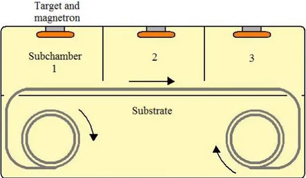
S-Solar has five vacuum chambers for sputtering, assembled by the company itself. These weigh about 3 metric ton each, and measure approximately 2x2x0.5 meters, excluding the vacuum pumps and power supply. They were fabricated between the years 1995 and 2006, and since then some minor changes and improvements have been made to them.
The chambers are connected to three different vacuum pumps: one rotary pump which acts as forepump (E2M80) with a capacity of 80 m3/h, after that a root pump (EH500A) and finally a
diffusion pump (HT16). Process parameters such as pressure, band speed, power etc. are controlled by a computer system that also stores a log file after each run containing the process parameters of that run at an arbitrary, pre-set band length interval.
The substrate used in the process is aluminium strips, almost 15 cm wide and 1,100 m long. A strip is loaded into the vacuum chamber on a coil, and during the sputter process they are unwound and pass underneath the magnetrons, before being wound back up on a second coil, similar to the motion of the tape in a tape-recorder. The strip usually moves with a speed of 1 m/min.
the deposition of one of the three different layers. The magnetron targets are located approximately 10 cm above the substrate. The targets are circular, and to prevent more material from depositing on the middle of the strips, the magnetrons are slightly shielded with a plate having a semicircular end. See Figure 1.5 for a simple and schematic picture of the sputter chambers at S-Solar.
Figure 1.5. Schematic view of a magnetron sputtering vacuum chamber at S-Solar. S-Solar uses DC planar magnetron sputtering.
The magnetrons are removed and cleaned after each run since a lot of sputtered material deposit on them as well. S-Solar has about 25 different magnetrons to be used in the five sputters with three magnetrons in each, thus having almost two full sets. At present, the magnetrons are not used in the same sputter each time, but instead they circulate. However, they are marked, and documentation makes it possible to track where and when a certain magnetron was used.
When assembling the strips into solar panels, one can either weld a copper tube to the back of the panel, or use a kind of “integrated” tube, in which case two aluminium plates are rolled together in a rolling mill with a copper tube in between them before sputtering. The high pressure force in the rolling process makes the aluminium and copper bond tightly, giving excellent heat conduction between the materials. After rolling, the strips are washed in a three-step custom-made washing machine to remove oil and dirt. In the first washing step, the strips are cleaned using high-pressure heated water and a diluted phosphorous detergent. In the second step, the strips are rinsed, and in the third step, dried.
After sputtering, the aluminium/copper strip is cut in shorter pieces and the flat copper tube is inflated using compressed air. The inflated copper tube is now not completely circular, but rather rhomb-shaped, which will cause turbulence in the water during operation. This will improve the heat conduction further since the heated water next to the tube walls will mix with the cooler water in the middle.
The desired absorption and thermal emission values of the S-Solar coatings are 96% ± 2% and 7% ± 2%, respectively. Since the start in the late 1990's, they have been working on improving the performance, but the process proved to be very complicated due to the large amount of parameters involved and the way these are related to each other.
The improvement efforts at S-Solar is partly empirical and partly based on the theory presented in the dissertations by Gelin and Zhao [1, 2]. The unique conditions at S-Solar often makes the general theory and the papers published on the subject of sputtering not very useful. Instead, the main source
of theoretical information has been the dissertations by Gelin and Zhao at Uppsala University who earlier have been working in cooperation with S-Solar.
These two dissertations are still very relevant, but the results cannot be transferred directly to the S-Solar production lines due to some differences in the set-ups. In the dissertations, sputter chambers with only one magnetron was used, thus depositing only one layer at a time. Sputtering the three layers one-by-one makes the process too slow to be used commercially, and so, at S-Solar, the layers must be sputtered in sequence in different sub-chambers. The sub-chambers cannot be completely isolated from each other since the aluminium strip is moving through them, and so, some of the gases will leak from one sub-chamber to the next. This makes the process more complicated, and so, unfortunately, the available theory does not always accord with the production at S-Solar.
Figure 1.6. One of the magnetron sputtering vacuum chambers at S-Solar.
2 Theory
2.1 Performance Determination
In our case, four quantities are of special interest when discussing electromagnetic radiation and its interaction with matter. These are the absorptance A(λ), reflectance R(λ), transmittance T(λ) and emittance E(λ). The absorptance, reflectance and transmittance are the fractional part of the incident light, at a certain wavelength, that is absorbed, reflected or transmitted, respectively. Emittance is defined as the ratio between the light emitted from the surface of interest to that emitted from a perfect blackbody source at the same wavelength and temperature.
Energy conservation gives
A λ R λT λ =1 , (2.1)
and, according to Kirchhoff´s law, the emittance is equal to the absorptance [3]
E λ =A λ =1− R λ −T λ . (2.2) To evaluate the performance of a solar absorber one uses the total solar absorptance, αs, and the total
thermal emittance, εt, as mentioned in the introduction. The total solar absorptance is a weighted
average, weighted by the solar spectral radiation, Is(λ), at a normal angle of incidence:
s=
∫
1 2
1− R
Isd ∫
1 2 Isd . (2.3)AM1.5 is used according to the ISO standard 9845-1 (1992).
The total thermal emittance is calculated at normal angle of radiation, and is also a weighted average, but weighted by the blackbody radiation spectrum, Ib(λ,T), for a given temperature T:
εt=
∫
λ3 λ4(
1− R(λ))
Ib(λ,T )d λ∫
λ3 λ4 Ib( λ,T )d λ , (2.4)where λ3 depends on the temperature and λ4 = 100 μm. For a temperature of 373 K, i.e., 100 ºC, λ3 = 2
μm, [1, 2].
At S-Solar, equipment for making very precise measurements are not available, and, instead, a portable measuring unit with a lower resolution is used. This instrument is an Optosol Absorber Control K unit, including an 'Alphameter' for absorptance measurements and an 'Emissiometer K' for emittance measurements.
The Alphameter is a very stable but low resolution spectrometer constructed for measurements on opaque solar absorbers. This spectrometer uses five light sources to illuminate the integrating sphere subsequently: four LEDs together with a silicon detector in the visible-IR range, and a tungsten halogen lamp in combination with a filtered germanium detector for wavelengths in the range from 1.2
to 1.9 μm. Since the spectra of solar absorbers often have smooth and gentle slopes, a low resolution spectrometer is well suited for these measurements.
The Emissiometer has an integrating sphere, a glowbar as a source of thermal radiation, and a detector sensitive for wavelengths in the range from 8 to 14 μm. The radiation is homogeneously distributed inside the sphere which serves as a diffuse radiation source, and the detector is installed at an angle of 10º to the normal of the sample surface. The Emissiometer is calibrated before each new measurement using one high and one low emittance calibration sample [4].
If a more detailed, full-spectrum analysis is desired, samples are sent to Ångströmlaboratoriet in Uppsala and S. Zhao. Zhao uses a Perkin-Elmer Lamda 900 UV/VIS/NIR double beam spectrophotometer for the absorption measurements, and a Tensor 27 from Bruker optic, measuring from 2.5 to 22 μm (450 cm-1) for the emittance measurements [5]. According to the standard EN 673,
the thermal emittance should be calculated covering at least up to 50 μm. The reflectance is therefore extrapolated to 100 μm.
2.2 Solid State Optics and Solar Absorber Design
The electric field of an electromagnetic plane wave travelling in some medium in the x-direction is described by
Em=E0exp
(
−k ωxc
)
exp(
iω t−n ω x
c
)
, (2.5)where Em is the amplitude of the field at position x and time t after entering the medium, ω is the
angular frequency, n and k is the real and imaginary part of the refractive index (N=n+ik), respectively,
and c is the speed of light in vacuum. The intensity I is proportional to Em2 and changes as I =I0e−α x
, (2.6)
where I0=|E0|2 is the intensity at x= 0. This gives an absorption coefficient, α, of
α=2 ω k
c =
4 ω k
λ , (2.7)
which means the intensity decreases logarithmically as
l n
II0
=−α d =−4 π k dλ , (2.8)
where d is the thickness of the film.
The extinction coefficient, k, is related to the so called intrinsic absorption, but thin films also have interference-induced absorption related to the refractive index n and the film thickness d. The factor kd/λ also determines at what wavelength the cross-over from low to high reflectance occurs, and so, choosing a proper combination of k and d is important in optimizing the solar absorber.
The extinction coefficient k can be changed if using composite films, by changing the filling volume ratio, the size or the shape of the composites. For homogeneous films, the factor kd/λ can only be changed by changing the thickness d.
As described by Equation 2.6, the amplitude of the em-wave decreases exponentially within an absorbing medium. In case of a thin film, we do not have that (αd)»1, and, consequently, light can be reflected at the bottom of the film and then re-reflected or transmitted at the top boundary, see Figure
2.1. This is the reason for the thin-film interference which will increase or decrease the front surface reflection, thus affecting the absorptivity, given that the boundaries are smooth and the film is homogeneous on a length scale larger than the wavelength of the light.
Figure 2.1. Thin film interference in the AR-coating. In a thin film, the reflected light can interfere to increase or decrease front surface reflections.
The thickness of the films can thus play a role in minimizing front surface reflections. Still, front surface reflections can be quite high due to the high refractive indices of the materials most often used in solar applications, and so an anti-reflection coating is often necessary. Fresnel formalism states that a transparent AR-coating on a surface of transparent material surrounded by vacuum should have a refractive index of
n=
ns, (2.9)where ns is the refractive index of the underlying material [1]. Results in Gelin's dissertation shows that
a refractive index of the AR-coating corresponding to the square root of that of the underlying material indeed gives the best solar absorptance. With a middle layer made from NiCr, a suitable AR-coating could, for instance, be NiCr with added CF4 gas, which is used by S-Solar, or SiO2.
When minimizing heat losses, the choice of substrate material is also very important. Metals like aluminium and copper are popular substrate materials since they fulfil the high infrared reflectance criteria. The reason for this high reflectance is the high concentration of free charge carriers which conduct electrical current and heat and are easily polarized by the light's high-frequency electric field. Unfortunately, the micro-climate in the solar absorber can corrode the aluminium and copper in the case the deposited films do not act protectively enough. To ensure long-term high quality it is, therefore, common to use a more corrosion protecting coating as the bottom-most layer, like nickel, chromium or alloys like CuNi, even though they will lower the infrared reflectance slightly. The CuNi and NiCr alloys used in the S-Solar solar absorbers have a very high corrosion resistance.
The degradation of the solar absorbers is mainly due to high temperatures, high humidity and moisture, airborne pollutants like sulphur dioxide, and the radiation from the sun. To ensure long-term high quality, good adhesion between substrate and film is crucial. The adhesion of the bottom-most CuNi layer on the aluminium substrate is generally good, but strongly dependent on the thickness of the layer, and possibly also on the applied electric power [1]. At S-Solar, adhesion is generally not a problem, provided there was no problem with the wash of the aluminium substrate before sputtering.
2.2.1 Process parameters
The optimization work done by Gelin and Zhao [1,2] revolves mostly around the oxygen flow, except an optimization by Gelin regarding the thermal emittance of the bottom-most layer as a function of the applied power and the argon pressure. According to Gelin, the lowest thermal emittance and films of the highest quality (dense, featureless structure) is, for CuNi, achieved for high power (1200 W) and low argon pressure (2.7·10-1 Pa). The same values cannot be expected to give the best results in the
S-Solar set-ups, but the results might follow the same pattern, with higher power and lower argon pressure giving a more dense film structure.
The amount of added oxygen (ml/min) is an important parameter in this process, and determines the degree of oxidation of the nickel particles. One way of characterizing this is by using the parameter relative oxygen gas flow, RO. It is defined as the amount of oxygen added relative to the amount of oxygen added at the transition point where the process changes from the metallic to the oxide sputtering mode, as mentioned in the Introduction. At this point, the target voltage drops suddenly, and target poisoning occurs. This is discussed further in Chapter 4, Results and Discussion.
The amount of oxygen that will give the best solar performance strongly depends on the applied power, and not as much on the argon flow. The tests performed by Gelin and Zhao [1, 2] implies that the best value of RO is 0.8, which then gives a sharper cross-over and, simultaneously, low reflectance in the UV-visible range.
At S-Solar, a couple of additional reactive gases are used, as mentioned above, and their flow rates will also, of course, play an important role when optimizing the process. There is not much scientific research concerning the impact of these gases on the solar panels, but employees at S-Solar has acquired some knowledge on how to manage these parameters.
Besides the final performance of the solar panels, the deposition process is also designed to give each panel an appealing deep blue colour. None of the constituent metals (copper, nickel and chromium) are in themselves blue, but interference mechanisms in the thin films, together with certain material properties, such as band structure of NiO, are believed to interact to create this visual appearance, though the process is not fully understood at present.
Pages 23 – 44 of the electronic version of this document is not available due to confidentiality reasons.
6 References
[1] Kristina Gelin, Preparation and Characterization of Sputter Deposited Spectrally Selective Solar Absorbers, Uppsala University (2004).
[2] Shuxi Zhao, Spectrally Selective Solar Absorbing Coatings Prepared by Magnetron Sputtering, Uppsala University (2007).
[3] Milton Ohring, Materials science of thin films, Academic Press (2002). [4] Personal communication with S-Solar.
[5] Personal communication with Shuxi Zhao.
[6] Swedish Energy Agency, http://energimyndigheten.se/en/Energy-efficiency/Household/Heating-your-home/Solar-heat/ alternatively http://energimyndigheten.se/sv/Hushall/Din-uppvarmning/Solvarme/
Appendix A - Purity of the Gases Used at S-Solar
Component Percentage
H2O < 0.5 ppm
Other gases < 0.5 ppm
Table A1.Contents of the oxygen gas used at S-Solar.
Component Percentage
H2O < 2 ppm
Other gases < 2 ppm
Table A2.Contents of the argon gas used at S-Solar.
Component Percentage
N2 < 20 ppm
Hydro carbon gases < 15 ppm
CO < 5 ppm
CO2 < 5 ppm
Other gases < 2 ppm
Table A3.Contents of the CF4 gas used at S-Solar.
Hydrogen gas is added to the process by using argon gas containing 2% hydrogen. This gas has in other aspects the same composition as the regular argon gas.