Alkali Dispersion in (Ag,Cu)(In,Ga)Se
2
Thin Film Solar Cells
Insight
from Theory and Experiment
Hisham Aboulfadl,*
Kostiantyn V. Sopiha, Jan Keller, Jes K. Larsen, Jonathan J.S. Scragg, Clas Persson,
Mattias Thuvander, and Marika Edoff
Cite This:ACS Appl. Mater. Interfaces 2021, 13, 7188−7199 Read Online
ACCESS
Metrics & More Article Recommendations*
sı Supporting InformationABSTRACT: Silver alloying of Cu(In,Ga)Se2 absorbers for thin film photovoltaics offers improvements in open-circuit voltage,
especially when combined with optimal alkali-treatments and certain Ga concentrations. The relationship between alkali distribution in the absorber and Ag alloying is investigated here, combining experimental and theoretical studies. Atom probe tomography analysis is implemented to quantify the local composition in grain interiors and at grain boundaries. The Na concentration in the
bulk increases up to∼60 ppm for [Ag]/([Ag] + [Cu]) = 0.2 compared to ∼20 ppm for films without Ag and up to ∼200 ppm for
[Ag]/([Ag] + [Cu]) = 1.0. First-principles calculations were employed to evaluate the formation energies of alkali-on-group-I
defects (where group-I refers to Ag and Cu) in (Ag,Cu)(In,Ga)Se2as a function of the Ag and Ga contents. The computational
results demonstrate strong agreement with the nanoscale analysis results, revealing a clear trend of increased alkali bulk solubility with the Ag concentration. The present study, therefore, provides a more nuanced understanding of the role of Ag in the enhanced performance of the respective photovoltaic devices.
KEYWORDS: ACIGS, CIGS, solubility limit, atom probe, density functional theory,first-principles calculations
1. INTRODUCTION
Cu(In,Ga)Se2(CIGSe) photovoltaics is a promising
technol-ogy combining high power conversion efficiency (PCE),
relatively low production cost, excellent outdoor stability,
and high radiation hardness.1,2One effective way of enhancing
the device performance is by tuning the bandgap energy (Eg)
at different parts of the absorber via adjusting the absorber
composition profiles, which in effect also improves band
alignment and suppresses recombination at interfaces. CIGSe is thermodynamically stable within a wide range of chemical compositions at usual deposition temperatures, allowing
bandgap engineering by alloying,3 which motivates the efforts
to further boost the PCEs. Tailoring of Eg by alloying can be
achieved during processing through varying the composition of the quaternary alloy, typically the [Ga]/([Ga] + [In]) ratio (referred to as GGI), incorporation of an additional alloying
element (such as Al, Ag, S, or Te), or combinations thereof.4
For CIGSe, the band gap varies from∼1.0 eV for CuInSe2to
∼1.7 eV for CuGaSe2,
5
making the alloy suitable not only for single-junction solar cells but also for tandem applications.
Alloying with Ag to form (Ag,Cu)(In,Ga)Se2(ACIGSe) allows
lowering the deposition temperature because of a reduction of
the melting point,6an improvement of the crystal quality,7,8an
increase in the carrier collection length,9and an enhancement
of the open-circuit voltage (VOC).10−13 Ag substitutes Cu in
the lattice structure, which decreases the p−d hybridization,
inducing a downward shift of both band edges and a slight
band gap widening.8 It has been established that an [Ag]/
([Ag] + [Cu]) value (referred to as AAC) of approximately 0.2
(at a GGI value of∼0.45) is optimal for improving the PCE of
single-junction solar cells.9 Hence, ACIGSe is a highly
interesting chalcogenide alloy that may eventually outcompete Received: November 17, 2020
Accepted: January 25, 2021 Published: February 3, 2021
Research Article
www.acsami.org
© 2021 The Authors. Published by
License, which permits unrestricted use, distribution and reproduction in any medium, provided the author and source are cited.
Downloaded via UPPSALA UNIV on April 6, 2021 at 07:10:08 (UTC).
CIGSe if the merits of the Ag addition for PCE offset the higher cost of raw materials.
Addition of alkali elements into the CIGSe absorber bulk or at its surface is another common practice because of the
positive effect on device performance.14,15Increased VOC and
fill factor (FF) are frequently reported for alkali-treated devices, stemming from the increased hole carrier density (improved conductivity) and presumably grain boundary (GB)
passivation optimizing local band bending.16,17Alkali elements
have limited solubility in CIGSe grain interiors (GIs),18 with
preferential segregation to lattice defects and phase boundaries
in the polycrystalline film.19 This is especially apparent for
heavy alkali elements (referring to K, Rb, or Cs) because of the
higher defect formation energies and increased diffusion
barriers in bulk CIGSe.20 Nonetheless, because the volume
fraction of GBs is small compared with that of the GIs, the
integral Na amounts can be comparable.21An ambiguity with
bulk incorporation, however, is that the most stable
alkali-on-Cu defects (AlkCu) are charge neutral, and thus electrically
inactive.20 In an attempt to reconcile these results with the
observed changes in the hole concentration,22a kinetic model
of alkali out-diffusion from GIs to GBs upon cooling was
developed.23 The situation became even more complicated
when a combination of Na with heavy alkali treatments demonstrated even higher PCEs in CIGSe compared to
single-alkali postdeposition treatment (PDT).24 Studies on the
diffusion mechanism of alkali elements in CIGSe have shown
that an interplay occurs between light (referring to Li and Na) and heavy alkalis regarding their distribution in the GIs and at
GBs, which is influenced by the substrate temperature as well
as the alkali supply dose.22 There is still an ongoing debate
whether the positive effects of alkali incorporation are related
to their dispersion in the GIs or GBs, as well as their
modification of the absorber surface.23,25 Furthermore, it is
reasonable to suppose that the incorporation and influences of
alkali elements could vary when the CIGSe absorber is
modified by Ag alloying, as described above.
Alkali elements can be introduced via predeposition treatment (alkali-containing precursor layer), coevaporation, or PDT, where the light and/or heavy alkali elements can be
chosen.4For heavy alkali elements, PDT is the most common
supply technique, whereas light alkali elements can be supplied with all three techniques. Substantial incorporation of alkali
elements is also caused by in-diffusion from glass substrates
during processing if no diffusion barrier is used. Irrespective of
the selected alkali element or doping technique, it has been shown that there is an optimum alkali amount, which if
exceeded leads to degradation of VOC and lower PCE values,
observed in both CIGSe and ACIGSe.26−29The effect seems
to be more severe in the case of ACIGSe, where the PCE can
drop significantly.30It has also been reported for Ag-alloyed
CuInSe2 (ACISe).31 This could be anticipated because the
optimum amount of KF PDT for ACIGSe was found to be lower compared to CIGSe synthesized under similar
conditions.10,26 Understanding the underlying cause of this
distinction is critical to further development of successful PDT strategies. Although the reason for this variance is currently
unknown, it could be because of the differences in (1)
solubility limits for alkalis (i.e., a thermodynamic effect) or (2)
rate of in-diffusion from the alkali-rich source (i.e., a kinetic
effect). There are some studies supporting both hypotheses.
Kim et al.11 showed using secondary ion mass spectrometry
(SIMS) that the Na concentration in the absorber increases upon addition of Ag in CIGSe grown on soda-lime glass (SLG) substrates, with the authors arguing in favor of faster
in-diffusion of alkalis in ACIGSe. However, in a more recent
study of ACIGSe/CIGSe tandem devices,12the same authors
presented SIMS profiles with nearly an order of magnitude
stronger Na signal within the ACIGSe top layer compared to the CIGSe bottom cell. Considering that the only source of alkalis was the SLG substrate, all Na in the top cells must have
diffused through the bottom CIGSe cell first. As such, the
preference for Na accumulation in the top ACIGSe cell points to higher alkali solubility in ACIGSe.
It, therefore, remains unclear how alkali elements are distributed in ACIGSe and what role they play in enhancing the performance of CIGSe devices upon Ag alloying. Among the few experimental techniques capable of investigating local compositions of GBs and GIs, atom probe tomography (APT) has been proven exceptionally useful for quantitative elemental
mapping in three dimensions.19,21,32−45To utilize this unique
capability, we perform in this work a comparative APT characterization of alkali distributions in polycrystalline
ACIGSe and CIGSe films. Additionally, we employ
first-principles calculations within the density functional theory (DFT) to verify and explain the experimental trends in solubility. With the synergy of these methods, we can draw a clearer picture of the complex phenomena behind the
improved efficiency of ACIGSe and CIGSe absorbers with
alkali incorporation.
2. EXPERIMENTAL AND COMPUTATIONAL METHODS
2.1. Solar Cell Processing. Two different glass substrates were used, namely SLG, which is Na-rich and high-strain glass (HSG), which is K-rich. Mo back contacts were DC-sputtered (target purity 99.97%) on the cleaned glass substrates, followed by evaporation of ∼15 nm thick NaF alkali precursor layers. CIGSe, ACIGSe, and Ag(In,Ga)Se2(AIGSe) absorbers were coevaporated in a three-stage Figure 1.Schematic illustration of the samples studied.
process using metal targets (99.999% purity) and 4N Se target (99.99% purity). The three-stage process follows an evaporation profile consisting of I-poor, I-rich, and finally I-poor stages, with all stages having the same [Ag]/[Cu] ratio for ACIGSe. The CIGSe (Ag-free, AAC = 0) and AIGSe (Cu-(Ag-free, AAC = 1) devices grown on SLG were produced here to be used for comparison (reference samples). The substrate temperature was about 400°C in the first stage and ramped up to about 550 °C in the following two stages. The deposition time for the absorber layers was about 30 min, resulting in film thicknesses of around 2 μm. High-Ga and low-In deposition rates were used at the initial stage of the absorber deposition to induce a Ga grading at the back contact. The elemental AAC, GGI, and ([Ag] + [Cu])/([Ga] + [In]) ([I]/[III]) ratios in the absorbers were determined using X-ray fluorescence (XRF) spectroscopy. KF PDT was performed on all samples for 10 min after ramping down the substrate temperature to 350°C at a rate of approximately 5 °C/min. A 40 nm CdS buffer layer was deposited using chemical bath deposition (CBD). A 125 ml solution with 4.5 mM Cd acetate and 1.7 M ammonium hydroxide was preheated in a 60°C water bath, after which 50 mL of thiourea (0.35 M) was added and the samples were immersed. The CdS growth was terminated after 6 min, after which the samples were rinsed and dried. Schematic of the four samples investigated is shown inFigure 1. Devices used for electronic measurements were completed by depositing a front stack of 100 nm of undoped ZnO, followed by 200 nm of ZnO/Al using RF magnetron sputtering (both targets of 99.99% purity). A metal stack of Ni−Al−Ni was deposited by electron beam evaporation through a shadow mask (target purity: 99.9% Ni and 99.999% Al). Finally, cells with an area of 0.5 cm2were defined by mechanical scribing. JV data are extracted from standard test conditions. All measurements were done sweeping from low to high voltage, with no significant hysteresis effects observed. The temperature during measurements was controlled to 25°C by a metal plate cooled with a Peltier element (no preconditioning used). Illumination was made using a halogen light calibrated to a photonflux corresponding to 1000 W/m2with a calibration Si solar cell. External quantum efficiency (EQE) measurements were carried out and the EQE intensity was used to calculate the current density under short circuit conditions using the data for AM1.5 spectral distribution.
2.2. Materials Characterization. Glow discharge optical emission spectroscopy (GDOES) elemental profile measurements were performed on the devices in a Spectruma Analytik GDA 750 HR system. A dual-beam focused ion-beam/scanning electron microscope (FIB/SEM) instrument (Thermo-Fisher Versa 3D) was used to carry out site-specific specimen preparations for APT analysis via a standard lift-out technique.46 Absorbers without front contacts (incomplete devices) were used for GDOES and APT characterization. A 100 nm thick Pt layer was deposited on top of the CdS layer using the electron beam in the FIB/SEM to minimize Ga-implantation. An acceleration voltage of 2 kV was used in thefinal steps of tip shaping to reduce Ga-implantation and surface amorphization effects. Laser-pulsed APT measurements were carried out using a LEAP 3000X HR CAMECA system using a green laser (λ = 532 nm) with a laser power set to 0.05 nJ, a repetition rate of 100 kHz, and base temperature of∼50 K. 3D reconstructions and data analysis were performed using CAMECA IVAS 3.6.14 software.
2.3. Computational Details. The first-principles calculations were carried out within DFT using the Vienna Ab initio Simulation Package (VASP).47−49The projector augmented wave pseudopoten-tials50,51 with valence electron configurations of 4d105s1 for Ag, 3d104s1for Cu, 4d105s25p1for In, 3d104s24p1for Ga, 4s24p4for Se, 3s1 for Na, 3p64s1 for K, 4p65s1 for Rb, and 5s25p66s1 for Cs were employed. The calculations were performed with the Perdew− Burke−Ernzerhof (PBE) exchange−correlation functional.52 All ACIGSe supercells contained 216 atoms with random occupation of the cationic sites (placing Ag/Cu on group-I and In/Ga on group-III positions) and were generated using the special quasirandom structure (SQS) algorithm,53as implemented in the Alloy-Theoretic Automated Toolkit (ATAT) package.54 The Brillouin-zone integra-tions were performed using a 2× 2 × 2 Γ-centered Monkhorst−Pack
grid55and a cut-off energy of 350 eV. The ionic and lattice relaxations were continued until reaching a threshold of 0.01 eV/Å on atomic forces. For the defect calculations, NaInSe2was simulated with the delafossite (R3̅m [#166]) structure, whereas KInSe2, RbInSe2, and CsInSe2 were modeled with a monoclinic (C2/c [#15]) cell. In contrast, the supercells of alkali alloys were initialized with a chalcopyrite structure but allowed to change symmetry during relaxation. The analysis was automatized using the Pymatgen library.56
3. RESULTS AND DISCUSSION
3.1. Absorber Composition and Device Performance. The absorber compositions were initially determined by XRF. The elemental AAC, GGI, and [I]/[III] of each sample are
presented in Table 1. Device characteristics of the respective
samples are presented inTable 2. For ACIGSe, the absorber
deposited on HSG showed slightly higher JSCand PCE values
compared to thefilms grown on SLG.
3.2. Alkali Distribution Profiles along the ACIGSe
Absorber Thickness. Figure 2 shows GDOES profiles of
alkalis in ACIGSe absorbers grown on the different substrates.
The profiles start at the CdS/ACIGSe interface and end in the
Mo layer. The absorber film grown on HSG was slightly
thinner compared to the one grown on SLG, with the
measured thicknesses of ∼1.7 and ∼2.1 μm, respectively
(determined by XRF and verified with cross-sectional SEM
images). Both films displayed an increase in Na and K
concentrations at the CdS/ACIGSe and ACIGSe/Mo interfaces. As expected, the K increase at the back contact is
more pronounced for the HSG substrate. Similar alkali profiles
were reported in our previous work for CIGSe and
ACIGSe,10,57as well as in multiple other studies reviewed in
ref22.
The main optoelectronic effects of alkali segregation at the
interfaces are suggested to be similar to those of alkalis dispersed in GBs, such as defect passivation and local band
bending.58 However, in addition, alkali enrichment at the
heterojunction can promote alkali-rich compound formation
(such as AlkInSe2),59 interactions with ordered defect
compound (ODC) phases,44,57as well as altering the growth
behavior of the buffer layer.58,60Surface chemical analysis was
performed here using energy-dispersive X-ray spectroscopy (EDS) in SEM and revealed no alkali-rich compounds, despite
the clear alkali enrichment identified at the absorber surface
using GDOES. Thus, the quantities of these compounds were below the sensitivity limit of EDS or they were not stable under the electron beam. In our previous study on alkali
treatment of ACIGSe,26 we demonstrated that the alkali-rich
surface compound, (Ag,K)InSe2, only begins to form in
samples treated with an excessive dose of KF. It is necessary to mention, however, that GDOES provides only qualitative analysis of the alkali distribution. Furthermore, it delivers in-depth compositional information averaged over a spot with a
diameter of ∼2 mm. Hence, interpretation of the GDOES
Table 1. Integral Absorber Compositions Measured with XRF
sample AAC GGI [I]/[III]
CIGSe-SLG 0 0.38 0.89
ACIGSe-SLG 0.22 0.40 0.89
ACIGSe-HSG 0.19 0.43 0.87
AIGS-SLG 1 0.40 0.85
scans should be made with caution. Local compositional analysis was performed here on the CdS/ACIGSe interface using APT, where alkali segregation was found to be inhomogeneous at the nanometer scale (see Figure S1 in
Supporting Information), that is, partial segregation occurs
across the entire interface. This indicates that at afine scale,
the alkali is most likely to be distributed as islands at the CdS/
ACIGSe interface. The alkali concentrations at the interface are well below 1 at. %, which is unfortunately not possible to
map using SEM−EDS, for instance.
It seems likely that the alkali segregation detected using GDOES near the surface is not connected with nucleation of ODCs because no clear group-I depletion is observed (not presented here). The formation of ODCs is governed by the
Table 2. Solar Cell Parameters for Selected Devices with the Standard Grid and without Antireflective Coatinga
sample VOC[mV] JSC[mA/cm2] FF [%] PCE [%]
CIGSe-SLG 704 (706± 3) 31.8 (30.7± 0.3) 75.3 (75.0± 1.2) 16.8 (16.3± 0.4)
ACIGSe-SLG 769 (761± 6) 30.2 (30.1± 0.2) 77.9 (74.8± 2.6) 18.1 (17.4± 0.7)
ACIGSe-HSG 770 (759± 10) 31.0 (30.7± 0.2) 77.7 (76.8± 0.6) 18.6 (17.9± 0.5)
AIGSe-SLG 682 (667± 5) 25.1 (24.4± 0.9) 68.2 (66.4± 1.7) 11.6 (10.7± 0.4)
aAverage values with their standard deviations are given in parentheses.
Figure 2.GDOES depth profiles for ACIGSe samples on (a) SLG and (b) HSG, showing K and Na signals from the CdS/ACIGSe interface to the Mo back contact. The onset of the Mo signal is marked in red color.
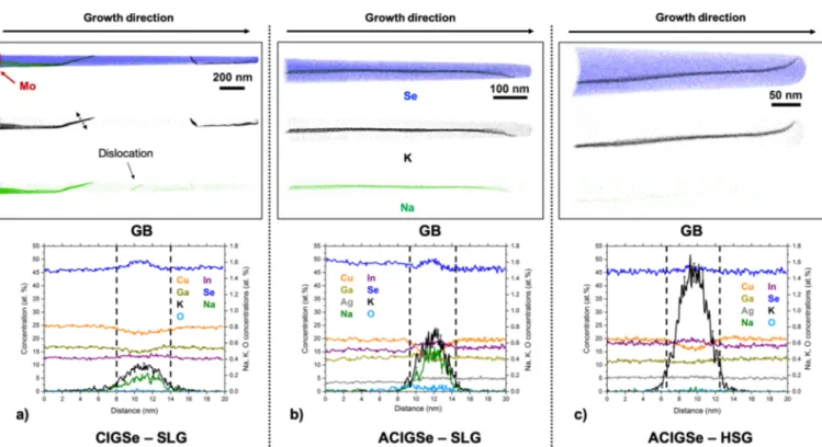
Figure 3. APT analysis of GBs in the CIGSe (SLG) and both ACIGSe samples. 1D concentration profiles are shown below the respective reconstructions. The uppermost reconstructions show overlaid Se (blue), K (black), and Na (green) atoms, with individual reconstructions for alkalis shown separately below. (a) CIGSe grown on SLG (reference) showing four GBs in the absorber and a Na-decorated dislocation. Some GBs appear thicker because the GB planes are not parallel to the viewing direction. The 1D profile is measured across the GB highlighted by dotted arrows. (b) ACIGSe grown on SLG and (c) ACIGSe grown on HSG, both showing one GB per reconstruction.
absorber composition, specifically the [I]/[III] ratio, as we
have recently shown for wide-gap ACIGSe.57
3.3. Nanoscale Analysis of Alkali Dispersion by Atom
Probe Tomography. In addition to GDOES depth profiling,
spatial distributions of the matrix and alkali elements in three dimensions were examined at the nanoscale using APT. The primary objective is analyzing the composition at GBs and in GIs, separately. Because of the limited volume analyzed using this technique and the compositional variations between
grains, a minimum offive successful APT measurements was
carried out from each sample with datasets of at least 10 million atoms, in order to attain reasonable statistics.
3.3.1. Grain Boundaries. The effect of Ag alloying on the GB composition and alkali dispersion is investigated here by analyzing the two ACIGSe samples and comparing them to the CIGSe absorber grown on SLG (Ag-free reference sample).
Figure 3 shows APT analyses of the three samples. Each presented 3D reconstruction includes at least one GB. In all
cases, the concentrations of matrix elements in the GBs differ
from those in the adjacent grains, which is a common
observation in CIGSe.32−35,38−40,42,45 The GBs here display
slight Cu-depletion and In-enrichment, which is especially evident for the ACIGSe samples. Interestingly, the measured
Ag profiles are almost flat, translating into an increasing AAC
ratio in the GBs. According to two earlier extensive APT
studies,42,61it is now understood that the majority of GBs in
CIGSe exhibit this kind of Cu-depletion. This tendency has also been reported using high-resolution XRF for CIGSe after
RbF PDT.62 The compositional fluctuations of matrix
elements at GBs are claimed to influence the electrical
characteristics of solar cells because of the local band
bending,63 which can have beneficial, detrimental, or neutral
impact on the device performance.32For instance, Cu-depleted
GBs are argued to reduce carrier recombination because they
act as hole barriers because of a downshift of the valence band
maximum.64Although structural information on planar defects
is usually not accessible by APT, the observed features resemble random high-angle GBs and not stacking faults or twin boundaries. Such a distinction can be made from an irregular curvature of interfaces, which stems from an arbitrary connectivity of faceted grains in the absorber.
Segregation of alkali elements at the GBs is observed for all samples. Both Na and K are found in dissimilar quantities at different GBs, which agrees with previous studies on
CIGSe.40,42,61 The effective thickness of the GBs, measured
by the compositional change at the interfaces, was in the range
of 4−6 nm (seeFigure 3). The extent of alkali segregation can
be additionally quantified by calculating the Gibbs interfacial
excess (Γ) values.65 The values were extracted for all GBs
shown inFigure 3. In the CIGSe sample, theΓNaandΓKvalues
varied among the four GBs recognized inFigure 3a from 0.03
to 2.74 at./nm2and from 0.97 to 3.14 at./nm2, respectively. In
the ACIGSe sample grown on SLG, theΓNaandΓKvalues in
the single GB seen inFigure 3b were 0.83 and 1.87 at./nm2,
respectively. For comparison, in the ACIGSe sample grown on
HSG, the ΓNa and ΓK values in the GB shown in Figure 3c
were 0.04 and 3.66 at./nm2, respectively. Traces of O were
detected at some GBs for each of the samples investigated,
which is a commonfinding in CIGSe and CZTS absorbers.66,67
Oxygen contamination is argued to arise primarily through
diffusion from the substrate and/or surface oxidation before
deposition of a buffer layer. Preferential O segregation is
reported for GBs with a specific misorientation angle,40but no
such correlation has been established for alkali elements.61
Herein, we observe no significant difference in the behavior of
alkalis at GBs of ACIGSe and CIGSe. However, three important observations can be made: (1) concentrations of
alkalis are dissimilar in different GBs within the same sample,
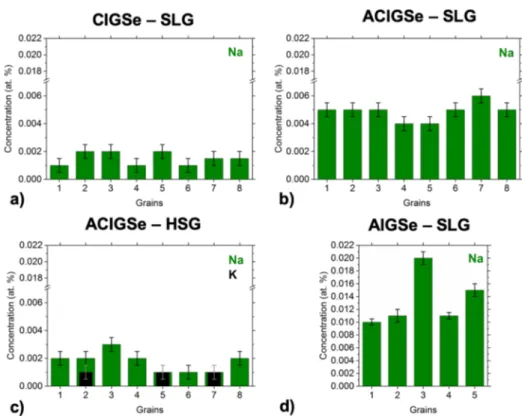
Figure 4.Alkali concentrations measured with APT in different grains of (a) CIGSe grown on SLG, (b) ACIGSe grown on SLG, (c) ACIGSe grown on HSG, and (d) AIGSe grown on SLG.
which is in agreement with earlier APT studies on
CIGSe.40,42,61(2) K segregation is more consistently observed
compared to Na, with some GBs being nearly devoid of Na,
even in the absorber grown on SLG, as seen inFigure 3a. (3)
GBs in the ACIGSe sample grown on the HSG substrate show greater K segregation and only small traces of Na. Hence, this indicates that the HSG substrate is clearly the leading source of K in the GBs. According to the model/hypothesis of interplay between light and heavy alkali elements in GBs and GIs of
chalcopyrite thin films (ion exchange mechanism),22,68 it is
understood that heavier alkalis replace Na at the GBs if
supplied in a higher dosage or if the films are deposited at
higher temperatures. This mechanism is expected to be driven by thermodynamic as well as kinetic factors. An increased concentration of K in the GBs because of a higher dosage is usually accompanied by segregations at the heterojunction, as observed here. It may lead to secondary phase formation (such
as KInSe2) on the absorber surface, which emphasizes that
interpretation of changes in device performance cannot solely
be based on alkali effects at the GBs. It is important to mention
that alkali-decorated GBs may have either detrimental or
benign effects on the cell efficiency depending on the
composition of the GBs, as reported in ref61. This highlights
the complexity of alkali effects in polycrystalline CIGSe (and
ACIGSe) and encourages investigating the alkali dispersion in the bulk, at the heterojunction and at the rear-interface simultaneously.
3.3.2. Grain Interiors.Figure 4 shows a plot for the alkali
concentrations measured with APT in eight different grains of
the CIGSe and ACIGSe samples, and infive different grains of
the AIGSe sample. Na is found to be widely distributed in the GIs, contrary to K, which is more localized at the GBs, especially when a higher dosage of K is introduced by using HSG, as shown above. These results are consistent with the ion
exchange mechanism for alkali elements.22,68 The
concen-tration of Na in the CIGSe reference sample varies from 10 to 20 ppm in the GIs, where the detection limit here in the
measurements is∼5 ppm. The Na concentrations in the GIs
for CIGSefit well into the range of values reported from APT
measurements in the literature for CIGSe and CuInSe2(CISe)
absorbers.34,36−38Such a consistency implies that Na reaches a
solubility limit in the CIGSe bulk. Exceptional cases can be found in the literature though, such as 148 ppm of Na in the
GIs of CIGSe reported by Choi et al.35using APT. In that case,
a fine-structured CIGSe absorber (high defect density) with
Na-containing defect clusters in the GIs was examined, which likely contributed to such a high level of Na. It is important to also point out that high alkali content values are sometimes
reported for CIGSe using SIMS analysis.21,69This quanti
fica-tion, however, should be treated with caution because SIMS cannot resolve alkali-enriched dislocations, stacking faults, and clustering, even if GBs and GIs are duly separated. These limitations render APT concentrations of alkalis more reliable
when resolution of different areas in a microstructure is
concerned. It is important to note that significantly fewer
decorated defects (such as dislocations) were detected using APT in the GIs of ACIGSe samples compared to the CIGSe sample. The specimen volume analyzed with APT is limited to evaluate defect densities and only decorated defects can be
identified, however, these observations may support the
arguments of suppressed formation of intragrain defects in
ACIGSe.7,70
The ACIGSe sample grown on SLG shows a clear increase in the Na content in the GIs. The Na concentration in this sample varies between 40 and 60 ppm, whereas the K concentration is below the detection limit. It is important to
note here that in the reconstruction shown inFigure 3b, it may
appear as if some K is detected in the GIs of this sample. This issue, however, is an artifact, which arises because of a small
peak overlap of 78Se2+ and 39K1+ at 39 Da in the mass
spectrum. Considering the natural isotope abundances, this peak overlap is deconvoluted in calculations of GI
compositions and 1D concentration profiles. For the ACIGSe
grown on HSG, Na concentration varies from 10 to 30 ppm
and some GIs show a K concentration of ∼10 ppm. APT
analysis of the AIGSe (Cu-free) sample grown on SLG revealed even higher Na concentrations in GIs reaching up to ∼200 ppm. Fewer grains were possible to examine for the AIGSe sample because of the mechanical instability of the APT specimens during measurements. This is likely stemming from
different mechanical properties of the AIGSe absorber (details
regarding specimen yield in APT analysis are discussed in ref
71). Hence, all results here point to an increase in the Na
solubility in GIs upon the addition of Ag in the chalcopyrite absorber. One can expect similar tendencies to exist for heavier alkalis because of similarities in their chemical properties to Na. However, concentrations of heavier alkalis are anticipated to be lower imposed by higher formation energies of
alkali-related point defects in GIs.20The maximum concentration of
Na detected in samples grown on SLG is plotted inFigure 5to
highlight the trend. As discussed inSection 1, the increase in
the alkali content is more likely to be of a thermodynamic
origin (higher solubility), which is investigated using
first-principles calculations in the next section.
3.4. Density Functional Theory Calculations. In order to compare the solubilities of alkali elements in ACIGSe and CIGSe, we utilized DFT for computing formation energies of
alkali elements on Cu or Ag site defects (AlkCuand AlkAg) as a
function of the alloy composition (i.e., GGI and AAC). We
only considered the substitutional defects because AlkCuis the
most stable alkali-related defect in CIGSe,20and is most likely
to remain dominant with addition of Ag. The defect formation energies were computed according to the following equation
μ μ
= − +
− + Δ − Δ
H E E E
E
(Alk ) (Alk ) (bulk) (I )
(Alk )
form
I tot I tot tot el
tot el I Alk (1)
where Etot(AlkI) and Etot(bulk) are the total energies of
ACIGSe with AlkCuand of the pristine supercell; Etot(Iel) and
Etot(Alkel) are the total energies (per atom) of group-I and Alk
elemental ground states; ΔμI and ΔμAlk are the chemical
Figure 5.Plot of the highest Na content measured by APT in each of the three samples grown on SLG with different AAC ratios.
potentials of group-I and Alk species with respect to those in the elemental ground states, respectively. The dependence on
the Fermi level and all corrections ineq 1are omitted because
of the charge-neutral nature of AlkCu.
To reproduce the stochastic nature of ACIGSe while avoiding large deviations in energies because of the multiplicity of possible cationic arrangements, the total energies of the supercells computed with DFT were processed with the cluster expansion (CE) formalism using the correlation functions of truly random systems. The CE for an alkali-free alloy was constructed from energies of 100 supercells generated using
the SQS algorithm, with compositions spanning the 0≤ GGI
≤ 1 and 0 ≤ AAC ≤ 1 range and a uniform 10 × 10 grid. In a similar manner, CEs for supercells containing defects were constructed for each alkali separately by replacing one randomly selected group-I cation (either Cu or Ag, whenever applicable) in the alloy supercell (yielding 180 nonequivalent systems). The results obtained without CE processing are
given in Supporting Information (see Figure S2) for
comparison.
To estimate the chemical potentials of elements in ACIGSe, we utilize the following relation
μ μ μ μ μ Δ = ·Δ + − ·Δ + ·Δ + − ·Δ + Δ H y y x x (ACIGSe) (1 ) (1 ) 2 f Ag Cu Ga In Se (2)
where x≡ GGI and y ≡ AAC in the equations. Obviously, in
contrast with the conventional methodology for defect
calculations,72 all chemical potentials and ACIGSe formation
energy (ΔHf(ACIGSe)) are functions of (x, y) composition.
Therefore, nontrivial thermodynamic considerations should be introduced. Herein, we extract an analytical expression for
ΔHf(ACIGSe) from our earlier study by setting T = 0 K in the
equation for free energy derived within the regular solution
approximation.73 This knowledge allows relating chemical
potentials as μ μ μ μ ∂Δ ∂ = Δ − Δ ∂Δ ∂ = Δ − Δ H x H y (ACIGSe) (ACIGSe) f Ga In f Ag Cu (3)
Combining eqs 2and3, one can obtain a system of three
equations withfive unknowns. The other two free variables can
be estimated from the stability diagrams according to the
well-established formalism for point defect calculations.72 Herein,
we present the results obtained for equilibrium between the
ACIGSe and AlkInSe2 phases. An alternative scenario of
equilibrium between ACIGSe and ODC was also explored and
discussed in theSupporting Information. Both approximations
provide qualitatively similar results, with only one exception specified below.
The choice of equilibrium with AlkInSe2phases is stipulated
by the established experimental knowledge. Specifically,
formation of AlkInSe2 crystals at CIGSe surfaces after alkali
treatments was reported for all four considered alkali elements
(Alk = Na, K, Rb, and Cs).74−77Such crystals are assumed to
be nearly Cu-free because AlkInSe2exhibits limited miscibility
with CuInSe2,74 even though Muzzillo et al.78 claimed
successful synthesis of (Cu,K)InSe2 alloys. These factors
constitute AlkInSe2 as a good system for extracting chemical
potentials for Ga-poor CIGSe.15,20In ACIGSe, the appearance
of (Ag,K)InSe2has been detected after KF PDT in our recent
work,26suggesting that a similar approximation can be applied
to Ag-alloyed CIGSe. With this in mind, an expression for the
formation energy of AlkInSe2can be written as
μ μ μ
ΔH (AlkInSe )f 2 = Δ Alk + Δ In+ Δ2 Se (4)
which can then be combined witheqs 2and3to yield
Figure 6.Computed formation energies of AlkCu(circle markers) and AlkAg(square markers) in ACIGSe in equilibrium with the AlkInSe2phase for (a) Alk = Na, (b) Alk = K, (c) Alk = Rb, and (d) Alk = Cs. The abscissa gives AAC values for supercells after substitution of the group-I element with the corresponding alkali. The series of curves represent ACIGSe alloys with different GGI values spanning the full range of compositions with equal intervals.
μ μ Δ − Δ = Δ − Δ − ·∂Δ ∂ − ·∂Δ ∂ H H x H x y H y (ACIGSe) (AlkInSe ) (ACIGSe) (ACIGSe) f Cu Alk f f 2 f (5)
and eq 5 can then be substituted in eq 1 for the defect
formation energy calculations in the case of AlkCu. Following
the same approach, a similar expression can be deduced for
ΔμAg − ΔμAlk and substituted ineq 1 to calculate formation
energies of AlkAg.
Figure 6 illustrates computed formation energies of AlkCu
and AlkAgwhen ACIGSe is in equilibrium with AlkInSe2. The
first thing to note there is that formation energies of AlkCuand
AlkAgfollow the same trends. This could be expected because
both defects represent the same imperfection in the crystal
lattice, AlkI. In other words, concentration of AlkIin the dilute
limit is defined by the formation energy, which must be
independent of the type of the substituted cation. In fact, the same total energies computed with DFT could be (but were
not) used for calculating formation energies of both AlkCuand
AlkAgby selecting an appropriate chemical potential (ΔμI) for
the formally substituted ion and the corresponding energy of
the elemental state (Etot(Iel)) in eq 1. The matching of the
formation energies is, therefore, not a material property but a validation of the employed methodology for defect calculations in random alloys.
More importantly, formation energies of all four considered alkalis decrease monotonically with AAC irrespective of GGI, meaning that their solubilities increase with Ag content. These
results are in good agreement with our APTfindings here and
previous studies reporting a higher Na content in ACIGSe.11,12
The formation energy demonstrates a stronger dependence on
AAC for heavier alkalis. For instance, the computed difference
in energy of NaI in CuInSe2 and AgInSe2 is only 0.23 eV,
whereas the corresponding values for KI, RbI, and CsIare 0.53,
0.66, and 0.78 eV, respectively. As for the absolute values, heavier alkalis have much higher formation energies (lower
solubilities), which is explained by the larger ions inflicting
more stress on the lattice.20 This is probably also the reason
why we did not detect any considerable K content in GIs with
APT, as it had probably diffused into the GBs during cooling.
At the same time, despite the decrease in formation energies upon Ag alloying, the solubility for Rb and Cs in GIs would possibly remain below the detection limit of APT if the absorbers were treated with Rb or Cs PDT. As such,
charge-neutral RbIand CsIare expected to play practically no role in
properties of bulk ACIGSe.
The formation energies increase slightly (but consistently) with GGI. This dependence is weaker compared to that on AAC and thus should be treated with more caution. This trend might even be invisible against random variations under the growth conditions, and hence, we did not attempt to verify it experimentally. The sensitivity of this result is evident, for
instance, as the formation energy of NaAg increases slightly
with GGI when Ag(Ga,In)Se2is in equilibrium with AlkInSe2
but decreases when an alternative approach assuming
equilibrium with ODC is considered (see Supporting
Information). Such a behavior is not surprising because the
equilibrium with AlkInSe2 compounds is, strictly speaking,
inapplicable to Ga-rich systems because other Alk containing Ga-rich phases would segregate in those systems instead. Despite this limitation, the computed dependences on AAC
are not strongly affected by the assumed equilibrium,
suggesting that both approximations are able to reasonably reproduce the actual chemistry of the alloy.
The computed energies can be used to estimate the ratio of
equilibrium NaIconcentrations in ACIGSe and CIGSe as
i k jjjjj y { zzzzz = − C C H H k T (Na ) (Na ) exp (Na ) (Na ) ACIGSe I CIGSe I
CIGSeform I ACIGSeform I
B (6)
Assuming equilibration during PDT at 350°C, the estimated
Na concentrations in ACIGSe with GGI = 0.3 and AAC of 0.2, 0.5, and 1.0 are roughly 4, 17, and 120 times higher than in CIGSe, respectively. Importantly, the predicted four-fold increase in the Na content for AAC = 0.2 is not far from
our chemical quantifications of GIs using APT. The value for
AAC = 0.5 is also in reasonable agreement with one order-of-magnitude higher Na content measured with SIMS in the top
ACIGSe cell of the tandem device fabricated by Kim et al.,12
but is lower than that reported in their earlier work,11possibly
because of the presence of impurity phases and/or variations under the growth conditions. In contrast, the predicted increase in the Na concentration for AAC = 1.0 does not
match the ∼10 times higher Na content from our APT
measurements on the Cu-free reference sample (seeFigure 5),
although the trend is correct on a qualitative level. A likely explanation for the discrepancy is that the maximum solubility is not reached during processing for this sample because much greater amount of Na from the substrate is required to saturate the absorber. Further analysis of this hypothesis from the perspective of alloy formation rather than the dilute limit approximation is provided below.
Figure 7.Computed mixing enthalpies for (Alk,Cu)InSe2and (Alk,Ag)InSe2alloys in the case of (a) Alk = Na and (b) Alk = K. The markers and lines represent the computed values and parabolicfits, respectively.
The observed trends in solubility versus AAC can be explained by a mismatch of ionic sizes of the group-I cations
and alkali impurities. According to Shannon,79 crystal ionic
radii of four-coordinated ions are 1.13 Å for Na1+, 1.51 Å for
K1+, 0.74 Å for Cu1+, and 1.14 Å for Ag1+. As one can see, the
Na1+ion is considerably larger than Cu1+but of the same size
as Ag1+, suggesting that Alk
I induces less stress on the lattice
and thus has lower formation energy (on average) in Ag-rich ACIGSe. The size mismatch increases for heavier alkalis, but it always remains smaller in Ag-based systems, resulting in a general tendency of increasing solubility with AAC.
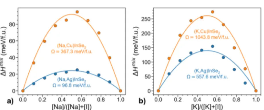
To further explore the role of lattice stress and consider the alkali incorporation beyond the dilute limit, we also computed
mixing enthalpies of (Na,Ag)InSe2, (Na,Cu)InSe2,
(K,Ag)-InSe2, and (K,Cu)InSe2alloys as
Δ = − ·
− − ·
−
H E x E
x E
(Alk Ag InSe ) (AlkInSe )
(1 ) (AgInSe )
x x mix
tot 1 2 tot 2
tot 2 (7)
where Etotrepresents computed total energies for supercells of
different compositions. The Ga-based alloys were not
considered because of the lack of structural information on
NaGaSe2 in the literature, which might be a sign of its
instability. The alloy interaction (bowing) parameters for
mixing enthalpies were extracted from parabolic fits to the
computed energy values, as shown in Figure 7. Furthermore,
the consolute temperatures (the points at which the alloys become fully miscible) were estimated from a regular solution
approximation as Tc = Ω/2kB. The obtained interaction
parametersΩ for the respective systems are 96.8, 367.3, 557.6,
and 1043.8 meV/f.u. (per formula unit), which yield consolute
temperatures of 288, 1858, 2962, and 5783°C, in agreement
with the earlier results for Cu-based chalcopyrites.15 As
expected, the mixing enthalpies are lower in Ag-based systems because of the aforementioned smaller ionic size mismatch. This tendency was also observed for Rb and Cs, but the corresponding mixing parameters are not extracted because of severe relaxation experienced by the alkali-rich supercells.
These consolute temperatures for all except (Na,Ag)InSe2
alloys are beyond the reach of synthesis as the chalcopyrite
systems melt at lower temperatures.80 As such, the wide
miscibility gap during processing clearly limits alkali solubility
for most systems. However, the exception of (Na,Ag)InSe2
means that this alloy can form during absorber deposition (550 °C) as well as during the PDT (350 °C). Practically, it means
that the solubility of Na in AgInSe2 absorbers is not
thermodynamically limited but instead governed by the processing parameters (primarily time and temperature
because of the thermally activated nature of Na in-diffusion
from the substrate), as we hypothesized above. Considering
that the dependence of NaI formation energy on GGI (see
Figure 6a) is weak, this conclusion can also be generalized to all AIGSe alloys, thereby explaining why the increase in the Na concentration in the Cu-free reference AIGSe sample deduced from the APT analysis was below the predicted equilibrium value.
4. CONCLUSIONS
In this work, we studied the relationship of Ag alloying in CIGSe on the alkali dispersion in bulk and at interfaces to better understand the enhancements in device performance related to the addition of Ag. Experimental analysis is
performed for ACIGSe absorbers deposited on two different
(K- and Na-rich) glass substrate types. The ion exchange mechanism commonly discussed in the literature for light and heavy alkali elements in CIGSe is observed for Na and K distributions in GBs and GIs. Alkali segregations at the CdS/ ACIGSe and rear interfaces, as well as in the GBs, were detected. K segregation appears to dominate over Na at the GBs in CIGSe and ACIGSe. While this behavior can be expected with the HSG substrate, simply because more K is supplied, stronger Na segregations would be expected when using the SLG substrate if not for the ion exchange mechanism. At the same time, GIs contain greater concentrations of Na than K, even for the absorber grown on the HSG substrate. This indicates higher solubility of Na in GIs compared to K. Furthermore, it is found that the Na concentration in the GIs increases with Ag-alloying. The nanoscale experimental
analysis was combined with first-principles calculations,
providing strong indications of increased solubility of alkali elements in GIs of ACIGSe compared to CIGSe. Such a behavior stems from a mismatch of ionic sizes of group-I
cations and alkali impurities, with Na1+ions, for instance, being
similar in size to Ag1+ but considerably larger than Cu1+, and
hence, inflicting less stress upon formation of NaIin Ag-alloyed
CIGSe. The same rationale applied to heavier alkali elements
as well. Hence, an increase in VOCof CIGSe devices with the
addition of Ag can be related to higher acceptance of alkali elements in the matrix, as well as improved band alignments and/or other factors discussed earlier. The fundamental
difference in alkali dispersion demonstrated here for
Ag-alloyed CIGSe absorbers should be taken into consideration when designing optimized alkali treatments in single- or multiple-junction solar cells using these types of absorbers.
■
ASSOCIATED CONTENT*
sı Supporting InformationThe Supporting Information is available free of charge at
https://pubs.acs.org/doi/10.1021/acsami.0c20539.
Local chemical analysis of the CdS/ACIGSe interface;
as-computed formation energies of AlkI in ACIGSe
supercells without additional processing with the CE formalism; defect formation energies assuming
equili-brium between (Ag,Cu)(In,Ga)3Se5 and ACIGSe with
the same AAC and GGI ratios; and primitive cell used
for simulation of (Ag,Cu)(In,Ga)3Se5 (in CIF format)
(PDF)
■
AUTHOR INFORMATION Corresponding AuthorHisham Aboulfadl− Division of Microstructure Physics,
Department of Physics, Chalmers University of Technology,
41296 Göteborg, Sweden;
orcid.org/0000-0003-2651-482X; Email:hisham.aboulfadl@chalmers.se
Authors
Kostiantyn V. Sopiha− Division of Solar Cell Technology,
Department of Materials Science and Engineering, Uppsala University, 75121 Uppsala, Sweden
Jan Keller− Division of Solar Cell Technology, Department of
Materials Science and Engineering, Uppsala University, 75121 Uppsala, Sweden
Jes K. Larsen− Division of Solar Cell Technology, Department
of Materials Science and Engineering, Uppsala University, 7196
75121 Uppsala, Sweden; orcid.org/0000-0002-7392-4701
Jonathan J.S. Scragg− Division of Solar Cell Technology,
Department of Materials Science and Engineering, Uppsala
University, 75121 Uppsala, Sweden;
orcid.org/0000-0001-8686-8721
Clas Persson− Center of Materials Science and
Nanotechnology, Department of Physics, University of Oslo, 0316 Oslo, Norway; Division of Applied Materials Physics, Department of Materials Science and Engineering, KTH Royal Institute of Technology, 10044 Stockholm, Sweden;
orcid.org/0000-0002-9050-5445
Mattias Thuvander− Division of Microstructure Physics,
Department of Physics, Chalmers University of Technology, 41296 Göteborg, Sweden
Marika Edoff − Division of Solar Cell Technology, Department
of Materials Science and Engineering, Uppsala University, 75121 Uppsala, Sweden
Complete contact information is available at:
https://pubs.acs.org/10.1021/acsami.0c20539
Funding
Swedish Foundation for Strategic Research, grant/award number: RMA15-0030.
Notes
The authors declare no competingfinancial interest.
■
ACKNOWLEDGMENTSThe computations and data handling were enabled by resources provided by the Swedish National Infrastructure for Computing (SNIC) at National Supercomputing Center (NSC) at Linköping University and PDC Center for High Performance Computing at KTH Royal Institute of Technol-ogy (projects: 2019/3-537 and 2019-3-381) partially funded by the Swedish Research Council through grant agreement no. 2018-05973.
■
REFERENCES(1) Ramanujam, J.; Singh, U. P. Copper Indium Gallium Selenide Based Solar Cells− a Review. Energy Environ. Sci. 2017, 10, 1306− 1319.
(2) Guillemoles, J. F. The Puzzle of Cu(In,Ga)Se2 (CIGS) Solar Cells Stability. Thin Solid Films 2002, 403−404, 405−409.
(3) Gloeckler, M.; Sites, J. R. Band-Gap Grading in Cu(In,Ga)Se2 Solar Cells. J. Phys. Chem. Solids 2005, 66, 1891−1894.
(4) Powalla, M.; Paetel, S.; Ahlswede, E.; Wuerz, R.; Wessendorf, C. D.; Magorian Friedlmeier, T. Thin-Film Solar Cells Exceeding 22% Solar Cell Efficiency: An Overview on CdTe-, Cu(In,Ga)Se2-, and Perovskite-Based Materials. Appl. Phys. Rev. 2018, 5, 041602.
(5) Wei, S. H.; Zunger, A. Band Offsets and Optical Bowings of Chalcopyrites and Zn-Based II-VI Alloys. J. Appl. Phys. 1995, 78, 3846−3856.
(6) Hanket, G. M.; Boyle, J. H.; Shafarman, W. N. Characterization and Device Performance of (AgCu)(InGa)2 Absorber Layers. 2009 34th IEEE Photovoltaics Specialists Conference, Philadelphia, PA, 2009; pp 001240−001245.
(7) Boyle, J. H.; McCandless, B. E.; Shafarman, W. N.; Birkmire, R. W. Structural and Optical Properties of (Ag,Cu)(In,Ga)Se2 Polycrystalline Thin Film Alloys. J. Appl. Phys. 2014, 115, 223504.
(8) Keller, J.; Sopiha, K. V.; Stolt, O.; Stolt, L.; Persson, C.; Scragg, J. J. S.; Törndahl, T.; Edoff, M. Wide-Gap (Ag,Cu)(In,Ga)Se2 Solar Cells with Different Buffer Materials A Path to a Better Heterojunction. Prog. Photovoltaics 2020, 28, 237−250.
(9) Shafarman, W.; Thompson, C.; Boyle, J.; Hanket, G.; Erslev, P.; Cohen, J. D. Device Characterization of (AgCu)(InGa)Se2 Solar Cells. 2010 35th IEEE Photovoltaics Specialists Conference, Honolulu, HI, 2010; pp 325−329.
(10) Edoff, M.; Jarmar, T.; Nilsson, N. S.; Wallin, E.; Hogstrom, D.; Stolt, O.; Lundberg, O.; Shafarman, W.; Stolt, L. High VOC in (Cu,Ag)(In,Ga)Se2 Solar Cells. IEEE J. Photovoltaics 2017, 7, 1789− 1794.
(11) Kim, K.; Park, J. W.; Yoo, J. S.; Cho, J.-s.; Lee, H.-D.; Yun, J. H. Ag Incorporation in Low-Temperature Grown Cu(In,Ga)Se2 Solar Cells Using Ag Precursor Layers. Sol. Energy Mater. Sol. Cells 2016, 146, 114−120.
(12) Kim, K.; Ahn, S. K.; Choi, J. H.; Yoo, J.; Eo, Y.-J.; Cho, J.-S.; Cho, A.; Gwak, J.; Song, S.; Cho, D.-H.; Chung, Y.-D.; Yun, J. H. Highly Efficient Ag-Alloyed Cu(In,Ga)Se2 Solar Cells with Wide Bandgaps and Their Application to Chalcopyrite-Based Tandem Solar Cells. Nano Energy 2018, 48, 345−352.
(13) Chen, L.; Lee, J.; Shafarman, W. N. The Comparison of (Ag,Cu)(In,Ga)Se2 and Cu(In,Ga)Se2 Thin Films Deposited by Three-Stage Coevaporation. IEEE J. Photovoltaics 2014, 4, 447−451. (14) Sun, Y.; Lin, S.; Li, W.; Cheng, S.; Zhang, Y.; Liu, Y.; Liu, W. Review on Alkali Element Doping in Cu(In,Ga)Se2Thin Films and Solar Cells. Engineering 2017, 3, 452−459.
(15) Siebentritt, S.; Avancini, E.; Bär, M.; Bombsch, J.; Bourgeois, E.; Buecheler, S.; Carron, R.; Castro, C.; Duguay, S.; Félix, R.; Handick, E.; Hariskos, D.; Havu, V.; Jackson, P.; Komsa, H. P.; Kunze, T.; Malitckaya, M.; Menozzi, R.; Nesladek, M.; Nicoara, N.; Puska, M.; Raghuwanshi, M.; Pareige, P.; Sadewasser, S.; Sozzi, G.; Tiwari, A. N.; Ueda, S.; Vilalta-Clemente, A.; Weiss, T. P.; Werner, F.; Wilks, R. G.; Witte, W.; Wolter, M. H. Heavy Alkali Treatment of Cu(In,Ga)Se2 Solar Cells: Surface versus Bulk Effects. Adv. Energy Mater. 2020, 10, 1903752.
(16) Granath, K.; Bodegård, M.; Stolt, L. Effect of NaF on Cu(In,Ga)Se2 Thin Film Solar Cells. Sol. Energy Mater. Sol. Cells 2000, 60, 279−293.
(17) Ruckh, M.; Schmid, D.; Kaiser, M.; Schäffler, R.; Walter, T.; Schock, H. Influence of Substrates on the Electrical Properties of Cu(In,Ga)Se2Thin Films. Sol. Energy Mater. Sol. Cells 1996, 41−42, 335−343.
(18) Kronik, L.; Cahen, D.; Schock, H. W. Effects of Sodium on Polycrystalline Cu(In,Ga)Se2 and Its Solar Cell Performance. Adv. Mater. 1998, 10, 31−36.
(19) Muzzillo, C. P.; Poplawsky, J. D.; Tong, H. M.; Guo, W.; Anderson, T. Revealing the Beneficial Role of K in Grain Interiors , Grain Boundaries , and at the Buffer Interface for Highly Efficient CuInSe2Solar Cells. Prog. Photovoltaics 2018, 26, 825−834.
(20) Malitckaya, M.; Komsa, H.-P.; Havu, V.; Puska, M. J. Effect of Alkali Metal Atom Doping on the CuInSe2-Based Solar Cell Absorber. J. Phys. Chem. C 2017, 121, 15516−15528.
(21) Wuerz, R.; Hempel, W.; Jackson, P. Diffusion of Rb in Polycrystalline Cu(In,Ga)Se2Layers and Effect of Rb on Solar Cell Parameters of Cu(In,Ga)Se2 Thin-Film Solar Cells. J. Appl. Phys. 2018, 124, 165305.
(22) Muzzillo, C. P. Review of Grain Interior, Grain Boundary, and Interface Effects of K in CIGS Solar Cells: Mechanisms for Performance Enhancement. Sol. Energy Mater. Sol. Cells 2017, 172, 18−24.
(23) Yuan, Z.-K.; Chen, S.; Xie, Y.; Park, J.-S.; Xiang, H.; Gong, X.-G.; Wei, S.-H. Na-Diffusion Enhanced p-Type Conductivity in Cu(In,Ga)Se2: A New Mechanism for Efficient Doping in Semi-conductors. Adv. Energy Mater. 2016, 6, 1601191.
(24) Pianezzi, F.; Reinhard, P.; Chirilă, A.; Bissig, B.; Nishiwaki, S.; Buecheler, S.; Tiwari, A. N. Unveiling the Effects of Post-Deposition Treatment with Different Alkaline Elements on the Electronic Properties of CIGS Thin Film Solar Cells. Phys. Chem. Chem. Phys. 2014, 16, 8843−8851.
(25) Urbaniak, A.; Igalson, M.; Pianezzi, F.; Bücheler, S.; Chirilă, A.; Reinhard, P.; Tiwari, A. N. Effects of Na Incorporation on Electrical
Properties of Cu(In,Ga)Se2-Based Photovoltaic Devices on Polyimide Substrates. Sol. Energy Mater. Sol. Cells 2014, 128, 52−56.
(26) Donzel-Gargand, O.; Larsson, F.; Törndahl, T.; Stolt, L.; Edoff, M. Secondary Phase Formation and Surface Modification from a High Dose KF-Post Deposition Treatment of (Ag,Cu)(In,Ga)Se2Solar Cell Absorbers. Prog. Photovoltaics 2019, 27, 220−228.
(27) Larsson, F.; Donzel-Gargand, O.; Keller, J.; Edoff, M.; Törndahl, T. Atomic Layer Deposition of Zn(O,S) Buffer Layers for Cu(In,Ga)Se2 Solar Cells with KF Post-Deposition Treatment. Sol. Energy Mater. Sol. Cells 2018, 183, 8−15.
(28) Feurer, T.; Fu, F.; Weiss, T. P.; Avancini, E.; Löckinger, J.; Buecheler, S.; Tiwari, A. N. RbF Post Deposition Treatment for Narrow Bandgap Cu(In,Ga)Se2Solar Cells. Thin Solid Films 2019, 670, 34−40.
(29) Caballero, R.; Kaufmann, C. A.; Eisenbarth, T.; Unold, T.; Klenk, R.; Schock, H.-W. High Efficiency Low Temperature Grown Cu(In,Ga)Se2Thin Film Solar Cells on Flexible Substrates Using NaF Precursor Layers. Prog. Photovoltaics 2011, 19, 547−551.
(30) Valdes, N. H.; Jones, K. J.; Opila, R. L.; Shafarman, W. N. Influence of Ga and Ag on the KF Treatment Chemistry for CIGS Solar Cells. IEEE J. Photovoltaics 2019, 9, 1846−1851.
(31) Valdes, N. H.; Lee, J.; Shafarman, W. N. Ag Alloying and KF Treatment Effects on Low Bandgap CuInSe2 Solar Cells. IEEE J. Photovoltaics 2019, 9, 906−911.
(32) Raghuwanshi, M.; Thöner, B.; Soni, P.; Wuttig, M.; Wuerz, R.; Cojocaru-Mirédin, O. Evidence of Enhanced Carrier Collection in Cu(In,Ga)Se2 Grain Boundaries: Correlation with Microstructure. ACS Appl. Mater. Interfaces 2018, 10, 14759−14766.
(33) Schwarz, T.; Stechmann, G.; Gault, B.; Cojocaru-Miredin, O.; Choi, P.; Redinger, A.; Siebentritt, S.; Raabe, D. Correlative Transmission EBSD-APT Analysis of Grain Boundaries in Cu-(In,Ga)Se2 and Cu2ZnSnSe4 Based Thin-Film Solar Cells. Microsc. Microanal. 2017, 23, 672−673.
(34) Colombara, D.; Werner, F.; Schwarz, T.; Cañero Infante, I.; Fleming, Y.; Valle, N.; Spindler, C.; Vacchieri, E.; Rey, G.; Guennou, M.; Bouttemy, M.; Manjón, A. G.; Peral Alonso, I.; Melchiorre, M.; El Adib, B.; Gault, B.; Raabe, D.; Dale, P. J.; Siebentritt, S. Sodium Enhances Indium-Gallium Interdiffusion in Copper Indium Gallium Diselenide Photovoltaic Absorbers. Nat. Commun. 2018, 9, 826.
(35) Choi, P.-P.; Cojocaru-Mirédin, O.; Wuerz, R.; Raabe, D. Comparative Atom Probe Study of Cu(In,Ga)Se2 Thin-Film Solar Cells Deposited on Soda-Lime Glass and Mild Steel Substrates. J. Appl. Phys. 2011, 110, 124513.
(36) Keller, J.; Schlesiger, R.; Riedel, I.; Parisi, J.; Schmitz, G.; Avellan, A.; Dalibor, T. Grain Boundary Investigations on Sulfurized Cu(In,Ga)(S,Se)2 Solar Cells Using Atom Probe Tomography. Sol. Energy Mater. Sol. Cells 2013, 117, 592−598.
(37) Cojocaru-Mirédin, O.; Choi, P.; Wuerz, R.; Raabe, D. Atomic-Scale Distribution of Impurities in CuInSe2-Based Thin-Film Solar Cells. Ultramicroscopy 2011, 111, 552−556.
(38) Vilalta-Clemente, A.; Raghuwanshi, M.; Duguay, S.; Castro, C.; Cadel, E.; Pareige, P.; Jackson, P.; Wuerz, R.; Hariskos, D.; Witte, W. Rubidium Distribution at Atomic Scale in High Efficient Cu(In,Ga)-Se2Thin-Film Solar Cells. Appl. Phys. Lett. 2018, 112, 103105.
(39) Cojocaru-Mirédin, O.; Choi, P.-P.; Abou-Ras, D.; Schmidt, S. S.; Caballero, R.; Raabe, D. Characterization of Grain Boundaries in Cu(In,Ga)Se2 Films Using Atom-Probe Tomography. IEEE J. Photovoltaics 2011, 1, 207−212.
(40) Cojocaru-Mirédin, O.; Schwarz, T.; Abou-Ras, D. Assessment of Elemental Distributions at Line and Planar Defects in Cu(In,Ga)-Se2Thin Films by Atom Probe Tomography. Scr. Mater. 2018, 148, 106−114.
(41) Cadel, E.; Barreau, N.; Kessler, J.; Pareige, P. Atom Probe Study of Sodium Distribution in Polycrystalline Cu (In,Ga)Se2Thin Film. Acta Mater. 2010, 58, 2634−2637.
(42) Stokes, A.; Al-Jassim, M.; Diercks, D.; Clarke, A.; Gorman, B. Impact of Wide-Ranging Nanoscale Chemistry on Band Structure at Cu(In, Ga)Se2Grain Boundaries. Sci. Rep. 2017, 7, 14163.
(43) Laemmle, A.; Wuerz, R.; Schwarz, T.; Cojocaru-Mirédin, O.; Choi, P.-P.; Powalla, M. Investigation of the Diffusion Behavior of Sodium in Cu(In,Ga)Se2Layers. J. Appl. Phys. 2014, 115, 154501.
(44) Stokes, A.; Al-Jassim, M.; Norman, A.; Diercks, D.; Gorman, B. Nanoscale Insight into the P-n Junction of Alkali-Incorporated Cu(In,Ga)Se2Solar Cells. Prog. Photovoltaics 2017, 25, 764−772.
(45) Cojocaru-Mirédin, O.; Schwarz, T.; Choi, P.-P.; Herbig, M.; Wuerz, R.; Raabe, D. Atom Probe Tomography Studies on the Cu(In,Ga)Se2Grain Boundaries. J. Visualized Exp. 2013, 74, 50376.
(46) Thompson, K.; Lawrence, D.; Larson, D. J.; Olson, J. D.; Kelly, T. F.; Gorman, B. In Situ Site-Specific Specimen Preparation for Atom Probe Tomography. Ultramicroscopy 2007, 107, 131−139.
(47) Kresse, G.; Furthmüller, J. Efficiency of Ab-Initio Total Energy Calculations for Metals and Semiconductors Using a Plane-Wave Basis Set. Comput. Mater. Sci. 1996, 6, 15−50.
(48) Kresse, G.; Furthmüller, J. Efficient Iterative Schemes for Ab Initio Total-Energy Calculations Using a Plane-Wave Basis Set. Phys. Rev. B: Condens. Matter Mater. Phys. 1996, 54, 11169−11186.
(49) Kresse, G.; Hafner, J. Ab Initio Molecular Dynamics for Liquid Metals. Phys. Rev. B: Condens. Matter Mater. Phys. 1993, 47, 558−561. (50) Kresse, G.; Joubert, D. From Ultrasoft Pseudopotentials to the Projector Augmented-Wave Method. Phys. Rev. B: Condens. Matter Mater. Phys. 1999, 59, 1758−1775.
(51) Blöchl, P. E. Projector Augmented-Wave Method. Phys. Rev. B: Condens. Matter Mater. Phys. 1994, 50, 17953−17979.
(52) Perdew, J. P.; Burke, K.; Ernzerhof, M. Generalized Gradient Approximation Made Simple. Phys. Rev. Lett. 1996, 77, 3865−3868.
(53) Zunger, A.; Wei, S.-H.; Ferreira, L. G.; Bernard, J. E. Special Quasirandom Structures. Comput. Mater. Sci. 1990, 65, 353−356.
(54) Van De Walle, A.; Tiwary, P.; De Jong, M.; Olmsted, D. L.; Asta, M.; Dick, A.; Shin, D.; Wang, Y.; Chen, L.-Q.; Liu, Z.-K. Efficient Stochastic Generation of Special Quasirandom Structures. CALPHAD: Comput. Coupling Phase Diagrams Thermochem. 2013, 42, 13−18.
(55) Chadi, D. J. Special Points for Brillouin-Zone Integrations. Phys. Rev. B: Solid State 1977, 16, 1746−1747.
(56) Ong, S. P.; Richards, W. D.; Jain, A.; Hautier, G.; Kocher, M.; Cholia, S.; Gunter, D.; Chevrier, V. L.; Persson, K. A.; Ceder, G. Python Materials Genomics (Pymatgen): A Robust, Open-Source Python Library for Materials Analysis. Comput. Mater. Sci. 2013, 68, 314−319.
(57) Keller, J.; Stolt, L.; Sopiha, K. V.; Larsen, J. K.; Riekehr, L.; Edoff, M. On the Paramount Role of Absorber Stoichiometry in (Ag,Cu)(In,Ga)Se2Wide-Gap Solar Cells. Sol. RRL 2020, 4, 2000508. (58) Ümsür, B.; Calvet, W.; Steigert, A.; Lauermann, I.; Gorgoi, M.; Prietzel, K.; Greiner, D.; Kaufmann, C. A.; Unold, T.; Lux-Steiner, M. C. Investigation of the Potassium Fluoride Post Deposition Treatment on the CIGSe/CdS Interface Using Hard X-Ray Photoemission Spectroscopy-a Comparative Study. Phys. Chem. Chem. Phys. 2016, 18, 14129−14138.
(59) Handick, E.; Reinhard, P.; Wilks, R. G.; Pianezzi, F.; Kunze, T.; Kreikemeyer-Lorenzo, D.; Weinhardt, L.; Blum, M.; Yang, W.; Gorgoi, M.; Ikenaga, E.; Gerlach, D.; Ueda, S.; Yamashita, Y.; Chikyow, T.; Heske, C.; Buecheler, S.; Tiwari, A. N.; Bär, M. Formation of a K-In-Se Surface Species by NaF/KF Postdeposition Treatment of Cu(In,Ga)Se2 Thin-Film Solar Cell Absorbers. ACS Appl. Mater. Interfaces 2017, 9, 3581−3589.
(60) Friedlmeier, T. M.; Jackson, P.; Kreikemeyer-Lorenzo, D.; Hauschild, D.; Kiowski, O.; Hariskos, D.; Weinhardt, L.; Heske, C.; Powalla, M. A Closer Look at Initial CdS Growth on High-Efficiency Cu(In,Ga)Se2 Absorbers Using Surface-Sensitive Methods. 2016 IEEE 43rd Photovoltaic Specialists Conference (PVSC), 2016; pp 457−461.
(61) Raghuwanshi, M.; Wuerz, R.; Cojocaru-Mirédin, O. Inter-connection between Trait, Structure, and Composition of Grain Boundaries in Cu(In,Ga)Se2Thin-Film Solar Cells. Adv. Funct. Mater. 2020, 30, 2001046.
(62) Schöppe, P.; Schönherr, S.; Jackson, P.; Wuerz, R.; Wisniewski, W.; Ritzer, M.; Zapf, M.; Johannes, A.; Schnohr, C. S.; Ronning, C.
Overall Distribution of Rubidium in Highly Efficient Cu(In,Ga)Se2 Solar Cells. ACS Appl. Mater. Interfaces 2018, 10, 40592−40598.
(63) Rau, U.; Taretto, K.; Siebentritt, S. Grain Boundaries in Cu(In,Ga)(Se,S)2 Thin-Film Solar Cells. Appl. Phys. A: Mater. Sci. Process. 2009, 96, 221−234.
(64) Persson, C.; Zunger, A. Anomalous Grain Boundary Physics in Polycrystalline CuInSe2: The Existence of a Hole Barrier. Phys. Rev. Lett. 2003, 91, 266401.
(65) Hellman, O. C.; Seidman, D. N. Measurement of the Gibbsian Interfacial Excess of Solute at an Interface of Arbitrary Geometry Using Three-Dimensional Atom Probe Microscopy. Mater. Sci. Eng., A 2002, 327, 24−28.
(66) Grini, S.; Sopiha, K. V.; Ross, N.; Liu, X.; Bjørheim, T. S.; Platzer-Björkman, C.; Persson, C.; Vines, L. Strong Interplay between Sodium and Oxygen in Kesterite Absorbers: Complex Formation, Incorporation, and Tailoring Depth Distributions. Adv. Energy Mater. 2019, 9, 1900740.
(67) Grini, S.; Aboulfadl, H.; Ross, N.; Persson, C.; Platzer-Björkman, C.; Thuvander, M.; Vines, L. Dynamic Impurity Redistributions in Kesterite Absorbers. Phys. Status Solidi B 2020, 257, 2000062.
(68) Chirilă, A.; Reinhard, P.; Pianezzi, F.; Bloesch, P.; Uhl, A. R.; Fella, C.; Kranz, L.; Keller, D.; Gretener, C.; Hagendorfer, H.; Jaeger, D.; Erni, R.; Nishiwaki, S.; Buecheler, S.; Tiwari, A. N. Potassium-Induced Surface Modification of Cu(In,Ga)Se2Thin Films for High-Efficiency Solar Cells. Nat. Mater. 2013, 12, 1107−1111.
(69) Jackson, P.; Wuerz, R.; Hariskos, D.; Lotter, E.; Witte, W.; Powalla, M. Effects of Heavy Alkali Elements in Cu(In,Ga)Se2Solar Cells with Efficiencies up to 22.6%. Phys. Status Solidi RRL 2016, 10, 583−586.
(70) Erslev, P. T.; Lee, J.; Hanket, G. M.; Shafarman, W. N.; Cohen, J. D. The Electronic Structure of Cu(In1‑xGax)Se2Alloyed with Silver. Thin Solid Films 2011, 519, 7296−7299.
(71) Prosa, T. J.; Strennen, S.; Olson, D.; Lawrence, D.; Larson, D. J. A Study of Parameters Affecting Atom Probe Tomography Specimen Survivability. Microsc. Microanal. 2019, 25, 425−437.
(72) Persson, C.; Zhao, Y. J.; Lany, S.; Zunger, A. N-Type Doping of CuInSe2 and CuGaSe2. Phys. Rev. B: Condens. Matter Mater. Phys. 2005, 72, 035211.
(73) Sopiha, K. V.; Larsen, J. K.; Donzel-Gargand, O.; Khavari, F.; Keller, J.; Edoff, M.; Platzer-Björkman, C.; Persson, C.; Scragg, J. J. S. Thermodynamic Stability, Phase Separation and Ag Grading in (Ag,Cu)(In,Ga)Se2 Solar Absorbers. J. Mater. Chem. A 2020, 8, 8740−8751.
(74) Hariskos, D.; Powalla, M. Thermodynamic Limitations for Alkali Metals in Cu(In,Ga)Se2. J. Mater. Res. 2017, 32, 3789−3800.
(75) Chen, J.; Shen, H.; Zhai, Z.; Liu, F.; Zhu, Z.; Luo, M. Performance and Stability Enhancement of Cu(InGa)Se2Solar Cells on Ultrathin Glass by Potassium Incorporation. Mater. Lett. 2020, 271, 127749.
(76) Taguchi, N.; Tanaka, S.; Ishizuka, S. Direct Insights into RbInSe2 Formation at Cu(In,Ga)Se2 Thin Film Surface with RbF Postdeposition Treatment. Appl. Phys. Lett. 2018, 113, 113903.
(77) Lin, T.-Y.; Khatri, I.; Matsuura, J.; Shudo, K.; Huang, W.-C.; Sugiyama, M.; Lai, C.-H.; Nakada, T. Alkali-Induced Grain Boundary Reconstruction on Cu(In,Ga)Se2Thin Film Solar Cells Using Cesium Fluoride Post Deposition Treatment. Nano Energy 2020, 68, 104299. (78) Muzzillo, C. P.; Mansfield, L. M.; Ramanathan, K.; Anderson, T. J. Properties of Cu1−xKxInSe2Alloys. J. Mater. Sci. 2016, 51, 6812− 6823.
(79) Shannon, R. D. Revised Effective Ionic Radii and Systematic Studies of Interatomic Distances in Halides and Chalcogenides. Acta Crystallogr., Sect. A: Cryst. Phys., Diffr., Theor. Gen. Crystallogr. 1976, 32, 751−767.
(80) Kühn, G.; Möller, W.; Engel, W. Heats and Entropies of Fusion of ABC2 Chalcopyrite Semiconductors. Thermochim. Acta 1984, 78, 129−134.