Linköping University Post Print
Spatially direct and indirect transitions of
self-assembled SiGe/Si quantum dots studied by
photoluminescence excitation spectroscopy
Bouchaib Adnane, Fredrik Karlsson, Göran Hansson, Per-Olof Holtz and Wei-Xin Ni
N.B.: When citing this work, cite the original article.
Original Publication:
Bouchaib Adnane, Fredrik Karlsson, Göran Hansson, Per-Olof Holtz and Wei-Xin Ni,
Spatially direct and indirect transitions of self-assembled SiGe/Si quantum dots studied by
photoluminescence excitation spectroscopy, 2010, Applied Physics Letters, (96), 18, 181107.
http://dx.doi.org/10.1063/1.3424789
Copyright: American Institute of Physics
http://www.aip.org/
Postprint available at: Linköping University Electronic Press
Spatially direct and indirect transitions of self-assembled GeSi/Si quantum
dots studied by photoluminescence excitation spectroscopy
B. Adnane,a兲K. F. Karlsson, G. V. Hansson, P. O. Holtz, and W.-X. Ni
Department of Physics, Chemistry, and Biology, Linköping University, S-581 83 Linköping, Sweden
共Received 21 December 2009; accepted 9 April 2010; published online 6 May 2010兲
Well-resolved photoluminescence excitation 共PLE兲 spectra are reported for self-assembled GeSi dots grown on Si共001兲 by molecular beam epitaxy. The observation of two excitation resonance peaks is attributed to two different excitation/de-excitation routes of interband optical transitions connected to the spatially direct and indirect recombination processes. It is concluded that two dot populations are addressed by each monitored luminescence energy for the PLE acquisition. © 2010
American Institute of Physics. 关doi:10.1063/1.3424789兴
Detailed knowledge on the electronic band structures, such as sublevels and related optical transitions, is very im-portant when using self-assembled GeSi quantum dots共QDs兲 embedded in Si for some applications in Si-based photonic devices.1During the past years, GeSi dot materials have been extensively studied by photoluminescence 共PL兲 measure-ments.2–5Due to inhomogeneous distribution of the size, al-loy composition, as well as local strain in the incorporated GeSi/Si dots, the observed dot-related luminescent emission was however rather broad, which thus hampered detailed studies of the electronic transitions involved in the luminescence.6,7
Based on careful analyses on the peak shape of temperature- and excitation power-dependent PL of GeSi dots, Larsson et al.8,9concluded that there were two different recombination processes related to the GeSi QDs. One was spatially direct within the dot, and the other one was spatially indirect across the interface between the dot and the sur-rounding Si in the type-II band alignment. Understanding and control of these effects are crucial for the improvement of the optical efficiency of this material system.
PL excitation共PLE兲 is known as a versatile tool useful in characterization of electronic states involved in the optical transitions with a better energy resolution. However, up to date, no PLE results from any GeSi/Si nanostructures have been published. In this letter, we report a study using PLE measurements with well-resolved excitation resonance peaks from self-assembled GeSi dots grown by molecular beam epitaxy 共MBE兲 on Si. By comparing with model calcula-tions, our PLE results were directly related to the coexistence of the spatially direct and indirect recombination processes, which therefore provided a more precise energy scheme of the subband states involved in these optical transitions.
The sample used for the optical studies was grown by solid-source MBE 共Balzers UMS-630兲. One Ge dot layer was formed via the Stranski–Krastanov growth mode by de-positing eight monolayers of Ge on a Si共001兲 substrate at a temperature of 530 ° C, and then capped with a 140 nm thick Si layer at 600 ° C in order to minimize incorporation of point defects. The average dot diameter was ⬃50 nm and
the typical height was⬃3 nm as measured by TEM, while the dot density was estimated to be about 4⫻1010 cm−2 by atomic force microscopy measurements9 on a reference sample without Si capping. The Ge content in the dots was determined to be at a level of⬃75% 共Ref.10兲 by means of
energy dispersive x-ray microanalysis.
The grown sample was characterized by both PL and PLE experiments. The PL was measured by a Fourier trans-form infrared spectrometer 共Bomem DA8兲 at 4 K using a 514 nm argon ion laser as the excitation source. The PLE measurements were excited by a picosecond optical paramet-ric oscillator 共OPO兲 synchronously pumped by a mode-locked Ti:sapphire laser, resulting in the spectrum-dependent output oscillation power with a maximum value at ⬃500 mW. The emission was spectrally dispersed by a 1 m double-grating monochromator, and measured by a liquid nitrogen-cooled Ge detector 共North Coast EO-817S兲 in the range of 0.7–1.4 eV using standard lock-in techniques. All PLE experiments were performed at low temperatures in a helium-bath cryostat.
A typical PL spectrum of the GeSi dot sample is depicted in Fig. 1, dominated by broadband emissions peaked at ⬃790 meV with a full width at half maximum 共FWHM兲 of ⬃60 meV. The spectral resolution of Fourier transform PL is high, allowing observation of the sharp boron-related TO replica PL at 1092 meV together with the multiple excitonic
a兲Author to whom correspondence should be addressed. Electronic mail:
bouad@ifm.liu.se. Present address: Department of Physics, Chemistry, and Biology, Linköping University, S-581 83 Linköping, Sweden. Tel.:⫹46 13 281182. FAX:⫹46 13 137568.
FIG. 1. 共Color online兲 PL spectrum of the GeSi/Si QDs measured at T = 4 K with an excitation power of 50 mW at=514 nm.
APPLIED PHYSICS LETTERS 96, 181107共2010兲
0003-6951/2010/96共18兲/181107/3/$30.00 96, 181107-1 © 2010 American Institute of Physics
emissions at 1090 meV and 1088 meV,11respectively, from the Si substrate. Besides, the broad emission around 1080 meV was due to recombination of electron-hole droplets, and the luminescence intensity dip at⬃0.9 eV was attributed to the quartz beamsplitter used in the measurement setup. No PL could be detected from the pseudomorphic Ge wetting layer 共WL兲 probably because of the carrier depletion effect associated with the high dot density that captured most of the carriers from the WL.12
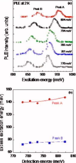
The PLE experiments were carried out by monitoring one section of the PL peak 共e.g., 788⫾2 meV兲 of the GeSi/Si QDs, and then scanning the excitation energies 共Eexc兲 with the OPO in the range of 800–1040 meV. Two
PLE peaks were observed at 928 meV and 862 meV, respec-tively, as marked by peak A and peak B in Fig. 2共a兲. The FWHM of the PLE peaks was ⬃20 meV, which is much smaller than that of the PL peak, meaning that only the dots with rather coherent properties共size, composition, and strain, etc.兲 could be monitored with the selected detection condition.
The PLE experiments were also performed at four dif-ferent detection energies along the up- and down-slope of the GeSi-dot PL peak, in order to probe the variation in transi-tion energies related to the electronic structure of different dot ensembles. One can see in Fig.2共a兲that the appearance
of the PLE spectra for different detection energies was very similar, while both peaks revealed a blueshift as the detection energy increased. This can be seen more evidently by plot-ting the excess excitation energy共⌬E=Eexc− Edet兲 as a
func-tion of the detecfunc-tion energy 共Edet兲 in Fig. 2共b兲 for all five PLE measurements.
As has been established, the electronic structure and ac-cordingly the optical transition energies of GeSi dots are in-fluenced by several factors such as dot size, composition, and strain.13In general, the PL observed at a higher energy could be caused by dots with either a smaller size or a lower Ge content. Assuming that the excitation would be mainly influ-enced by hole subbands in the GeSi dot, the corresponding excess excitation energy⌬E would however have a different trend. The ⌬E would increase with the reduction in dot size but it would decrease when decreasing the Ge content. Therefore, our observation of a small PLE energy increase with the increasing PL detection energy would be explained mainly due to the size effect, while partly compensated by the change in the Ge composition.
Moreover, the excitation power dependence of the PLE peak intensity was quite different between the measured ex-citation peaks A and B. By reducing the primary power of the OPO one order of magnitude lower using a neutral den-sity filter, the intenden-sity of peak A decreased by about 50%, but the intensity of peak B nearly vanished. The strongly different power dependences of the two PLE features is an indication that the detected PL would originate from two different recombination processes but coincidently with the same transition energy for the detected PL originating from two separate ensembles of GeSi dots.
According to the earlier PL work by Larsson et al.,8,9 there are two recombination processes in the GeSi/Si dot material system, corresponding to the spatially direct and indirect transitions, respectively, observed for specific ex-perimental conditions. The emission corresponding to the di-rect transition in the dot is solely observed at elevated tem-peratures and higher excitation power. The PL spectra in Fig.
1 are not measured under these particular conditions and ac-cordingly only the peak corresponding to the indirect transi-tion is expected in this case. Furthermore, it is concluded that the PL and PLE peaks are dominated by no-phonon transi-tions, i.e., associated with a relatively modest phonon cou-pling strength due to local lattice disordering introduced by alloy composition and strain variation across the dot partially relaxing the k-momentum conservation.
Hence the physical origin of the PLE peaks is attributed to three routes with respect to different transition processes, as illustrated by arrows and grouped by marks of PLE peak A, PLE peak B, and PLE peak C in the potential diagram in Fig.3 for a single GeSi dot.
The PLE peak A is proposed to correspond to a spatially direct transition in the GeSi dot between the light hole ground sublevel 共lh0兲 of the valence band and the ⌬4valley
of the conduction band, where the recombination between the ⌬4 electron state and the heavy hole ground sublevel
共hh0兲 is detected. The lower energy PLE peak B is
inter-preted as the spatially direct excitation from the hh0 state to
the⌬4valley inside the GeSi dot, when the spatially indirect recombination at the interface between a⌬2electron state in
the notch potential of the strained Si barrier layer and the hh0
state in the GeSi dot is detected. Therefore, within the
varia-FIG. 2.共Color online兲 共a兲 PLE spectra of GeSi/Si dots acquired at different detection energies at T = 2 K. The spectra are shifted vertically for clarity. 共b兲 Variation in the excess excitation energy 共⌬E兲 as a function of the de-tection energy for the two resonance peaks in the PLE spectra.
181107-2 Adnane et al. Appl. Phys. Lett. 96, 181107共2010兲
tion range of dot size, composition, and connected strain in the grown GeSi/Si dot material, it is possible to observe these two PLE peaks from two different subgroups of GeSi dots, when monitoring the PL at one single detection energy. Our model predicts also a third peak, denoted peak C in Fig.
3, which could not be resolved in the PLE spectra shown in Fig. 2共a兲. This is probably due to the fact that this peak is below the detection limit since the combined effects of the lower OPO power in the expected energy range and the weaker matrix elements for the LH0-⌬4transition compared
to the HH0-⌬4transition in the PLE as well as for the indirect transition monitored in PL. These combined effects are ex-pected to cause a lowered detected intensity by about one order of magnitude of peak C relatively to peaks A and B.
To support our interpretation of the experimental results, a numerical analysis of the electronic band structure of the GeSi/Si dots, with the three-dimensional strain distribution that was calculated by assuming isotropic elastic constants,14 was performed using a 6⫻6 band k·p approach for the va-lence band15–20 and solving the Schrödinger equation with anisotropic effective electron masses for the conduction band. Each QD was assumed to have a truncated-pyramid shape with the base orientation along the 关100兴 and 关010兴 directions. The pyramid base was fixed to 30 nm and the height was varied continuously from 2 to 4 nm. Because of the small aspect ratio共height/base兲 of the QDs, the quantum confinement effects are mostly determined by the dot height along the 关001兴 growth direction, which justifies that the QDs can, in a simplified picture, be modeled by local GeSi QWs embedded in Si.
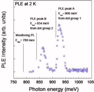
The computation results are presented in Fig.4 together with a PLE spectrum 关depicted as the middle one in Fig.
2共a兲兴 for comparison. It shows that with the detected PL energy at 788⫾2 meV, the spatially direct PL is to be ex-cited by a photon energy of 908 meV via route A from the GeSi dot with 78% of Ge at a dot height of 2.8 nm, while the spatially indirect PL共route B兲 could be observed by an ex-citation energy of 834 meV from the dot containing 75% Ge and 2.0 nm in height. These results are in a fairly good agree-ment with the experiagree-mental observations.
In summary, the first luminescence excitation spectra from self-assembled GeSi dots grown by MBE on Si are reported. By comparing with six-band k · p calculations for truncated pyramidal shape GeSi/Si QDs, our experimentally observed PLE features are assigned to be due to optical tran-sitions of two kinds involving the two following different dot populations: the spatially direct transition inside the GeSi dot and the spatially indirect transition across the Si/Ge inter-face. In fact, these two processes are coexisting in any single GeSi dot, and dispersed in a wide spectral range over all dots with a certain variation in size, composition, and strain, which consequently results in a broadband PL emission.
1K. Brunner,Rep. Prog. Phys. 65, 27共2002兲.
2P. Schittenhelm, M. Gail, J. Brunner, J. F. Nützel, and G. Abstreiter,Appl. Phys. Lett. 67, 1292共1995兲.
3H. Sunamura, N. Usami, Y. Shiraki, and S. Fukatsu,Appl. Phys. Lett. 66,
3024共1995兲.
4O. G. Schmidt, C. Lange, and K. Eberl,Appl. Phys. Lett.75, 1905共1999兲. 5V. Le Thanh, P. Boucaud, D. Débarre, D. Bouchier, and J. M. Lourtioz,
Phys. Rev. B 58, 13115共1998兲.
6S. Fukatsu, H. Sunamura, Y. Shiraki, and S. Komiyama,Appl. Phys. Lett.
71, 258共1997兲.
7G. Bremond, M. Serpentini, A. Souifi, G. Guillot, B. Jacquier, M.
Abdal-lah, I. Berbezier, and B. Joyce,Microelectron. J. 30, 357共1999兲.
8M. Larsson, A. Elfving, P. O. Holtz, G. V. Hansson, and W.-X. Ni,Appl. Phys. Lett. 82, 4785共2003兲.
9M. Larsson, A. Elfving, W.-X. Ni, G. V. Hansson, and P. O. Holtz,Phys. Rev. B 73, 195319共2006兲.
10A. Karim, A. Elfving, M. Larsson, W.-X. Ni, and G. V. Hansson,Proc. SPIE 6129, 61290C共2006兲.
11G. Davies,Phys. Rep. 176, 83共1989兲.
12E. S. Moskalenko, K. F. Karlsson, V. Donchev, P. O. Holtz, W. V.
Schoenfeld, and P. M. Petroff,Appl. Phys. Lett. 84, 4896共2004兲.
13O. G. Schmidt, K. Eberl, and Y. Rau,Phys. Rev. B 62, 16715共2000兲. 14G. S. Pearson and D. A. Faux,J. Appl. Phys. 88, 730共2000兲. 15M. Chandrasekhar and F. H. Pollak,Phys. Rev. B 15, 2127共1977兲. 16S. M. Sze and K. K. Ng, Physics of Semiconductor Devices共Wiley,
Hobo-ken, New Jersey, 2007兲.
17C. G. Van de Walle and R. M. Martin,Phys. Rev. B 34, 5621共1986兲. 18C. G. Van de Walle,Phys. Rev. B 39, 1871共1989兲.
19J. Weber and M. Alonso,Phys. Rev. B 40, 5683共1989兲. 20M. Rieger and P. Vogl,Phys. Rev. B 48, 14276共1993兲.
FIG. 3. Schematic band-edge diagram of the GeSi-dot/Si heterojunction along the z direction with the relevant interband transitions corresponding to the observed PLE peaks.
FIG. 4.共Color online兲 Comparison between calculated absorptions from two different dot populations共noted as dot group 1 and dot group 2兲 and an experimental PLE spectrum of the GeSi/Si dot with the PL detected at 788 meV. Calculated transitions are represented by bars in the figure.
181107-3 Adnane et al. Appl. Phys. Lett. 96, 181107共2010兲