Linköping Studies in Science and Technology Dissertation No. 1259
Reconfigurable and Broadband
Circuits for Flexible RF Front Ends
Naveed Ahsan
Electronic Devices
Department of Electrical Engineering
Linköping University, SE-581 83 Linköping, Sweden Linköping 2009
ISBN 978-91-7393-605-7 ISSN 0345-7524
Reconfigurable and Broadband Circuits for
Flexible RF Front Ends
Naveed Ahsan
Copyright © Naveed Ahsan, 2009 ISBN: 978-91-7393-605-7
Linköping Studies in Science and Technology Dissertation No. 1259
ISSN: 0345-7524 Electronic Devices
Department of Electrical Engineering Linköping University
SE-581 83 Linköping Sweden
Author’s e-mail: naveed@isy.liu.se navahsn@yahoo.com
About the cover:
Top left picture: illustration of a highly linear, wideband RF front-end for multi-standard receivers that can withstand large blockers. 90nm CMOS chip micrograph on right. 0.2µm GaAs chip micrograph (left) and illustration of PROMFA concept with its three key functions.
Cover designed by author.
Printed at LiU-Tryck, Linköping University Linköping, Sweden.
Abstract
Most of today’s microwave circuits are designed for specific function and special need. There is a growing trend to have flexible and reconfigurable circuits. Circuits that can be digitally programmed to achieve various functions based on specific needs. Realization of high frequency circuit blocks that can be dynamically reconfigured to achieve the desired performance seems to be challenging. However, with recent advances in many areas of technology these demands can now be met.
Two concepts have been investigated in this thesis. The initial part presents the feasibility of a flexible and programmable circuit (PROMFA) that can be utilized for multifunctional systems operating at microwave frequencies. Design details and PROMFA implementation is presented. This concept is based on an array of generic cells, which consists of a matrix of analog building blocks that can be dynamically reconfigured. Either each matrix element can be programmed independently or several elements can be programmed collectively to achieve a specific function. The PROMFA circuit can therefore realize more complex functions, such as filters or oscillators. Realization of a flexible RF circuit based on generic cells is a new concept. In order to validate the idea, two test chips have been fabricated. The first chip implementation was carried out in
a 0.2µm GaAs process, ED02AH from OMMICTM. The second chip was
implemented in a standard 90nm CMOS process. Simulated and measured results are presented along with some key applications such as low noise amplifier, tunable band pass filter and a tunable oscillator.
The later part of the thesis covers the design and implementation of broadband RF front-ends that can be utilized for multistandard terminals such as software defined radio (SDR). The concept of low gain, highly linear frontends has been presented. For proof of concept two test chips have been implemented in 90nm CMOS technology process. Simulated and measurement results are presented. These RF front-end implementations utilize wideband designs with active and passive mixer configurations.
We have also investigated narrowband tunable LNAs. A dual band tunable LNA MMIC has been fabricated in 0.2µm GaAs process. A self tuning technique has been proposed for the optimization of this LNA.
Preface
This dissertation presents my research work during the period from June 2005 to May 2009, at the Division of Electronic Devices, Department of Electrical Engineering, Linköping University, Sweden. This thesis is mainly based on the following publications:
• Paper 1: Naveed Ahsan, Aziz Ouacha, Carl Samuelsson and Tomas Boman “Applications of Programmable Microwave Function Array (PROMFA),” in Proceedings of the IEEE European Conference on Circuit Theory and Design (ECCTD 2007), pp. 164-167, August 26-30, 2007, Seville, Spain.
• Paper 2: Naveed Ahsan, Aziz Ouacha, Christer Svensson, Carl Samuelsson and Jerzy Dąbrowski “A Design Approach for Flexible RF Circuits Using Reconfigurable PROMFA Cells,” manuscript submitted in Journal of Analog Integrated Circuits and Signal Processing.
• Paper 3: Naveed Ahsan, Aziz Ouacha, Jerzy Dąbrowski and Carl Samuelsson “Dual band Tunable LNA for Flexible RF Front-End,” in Proceedings of the IEEE International Bhurban Conference on Applied Sciences & Technology (IBCAST 2007), pp. 19-22, January 8-11, 2007, Islamabad, Pakistan.
• Paper 4: Naveed Ahsan, Jerzy Dąbrowski and Aziz Ouacha “A Self Tuning Technique for Optimization of Dual Band LNA,” in Proceedings of the IEEE European Wireless Technology Conference (EuWiT), EuMW
• Paper 5: Naveed Ahsan, Christer Svensson and Jerzy Dąbrowski “Highly Linear Wideband Low Power Current Mode LNA,” in Proceedings of the IEEE International Conference on Signals and Electronic Systems (ICSES 08), pp. 73-76, September 14-17, 2008, KrakÓw, Poland.
• Paper 6: Rashad Ramzan, Naveed Ahsan, Jerzy Dąbrowski and Christer Svensson “A 0.5-6GHz Low Gain RF Front-end for Low-IF Over-Sampling Receivers in 90nm CMOS,” manuscript submitted in IEEE Transactions on Circuits and Systems-II: Express Briefs.
• Paper 7: Naveed Ahsan, Christer Svensson, Rashad Ramzan, Jerzy Dąbrowski, Aziz Ouacha, and Carl Samuelsson “A 1.1V 6.2mW, Highly Linear Wideband RF Front-end for Multi-Standard Receivers in 90nm CMOS,” manuscript submitted in IEEE Journal of Solid State Circuits. The following publications related to this research are not included in the thesis:
• Carl Samuelsson, Aziz Ouacha, Naveed Ahsan, Tomas Boman
“Programmable Microwave Function Array, PROMFA,” in Proceedings of the IEEE Asia-Pacific Microwave Conference 2006 (APMC 2006), pp. 1787-1790, December 12-15, 2006, Yokohama, Japan.
• Naveed Ahsan, Aziz Ouacha and Jerzy Dąbrowski “A Tunable LNA for Flexible RF Front-End,” Swedish System-on-Chip Conference (SSoCC06), May 4-5, 2006, Kolmården, Sweden.
• Naveed Ahsan, Aziz Ouacha, Carl Samuelsson and Tomas Boman “A Widely Tunable Filter Using Generic PROMFA Cells,” Swedish System-on-Chip Conference (SSoCC07), May 14-15, 2007, Fiskebäckskil, Sweden.
• Shakeel Ahmad, Naveed Ahsan, Anton Blad, Rashad Ramzan, Timmy
Sundström, Håkan Johansson, Jerzy Dąbrowski, and Christer Svensson, “Feasibility of Filter-less RF Receiver Front end,” Giga Hertz Symposium
vii I have also contributed in the following papers that are not related to this research:
• Ghulam Mehdi, Naveed Ahsan, Amjad Altaf, and Amir Eghbali “A
403-MHz Fully Differential Class-E Amplifier in 0.35µm CMOS for ISM Band Applications,” in Proceedings of the IEEE East-West Design Test Symposium (EWDTS 2008), pp. 239-242, October 9-12, 2008, Lviv, Ukraine*.
• Rashad Ramzan, Naveed Ahsan, and Jerzy Dąbrowski “On-Chip
Stimulus Generator for Gain, Linearity, and Blocking Profile Test of Wideband RF Front-ends,” manuscript submitted in IEEE Transactions on Instrumentation & Measurement.
Contributions
The main contributions of this dissertation are as follows:
• Design of reconfigurable circuits using PROMFA concept. To
demonstrate the viability of this approach, two test circuits have been implemented using 0.2µm GaAs and 90nm CMOS technology process.
• Design and implementation of a dual band tunable low noise amplifier in
0.2µm GaAs technology process. A self-tuning technique has been proposed for optimization of this LNA.
• Design and implementation of a wideband highly linear low noise
amplifier in 90nm CMOS.
• Design, implementation and testing of a low power, highly linear
wideband RF front-end for multistandard receivers in 90nm CMOS. The proposed front-end can withstand large blockers.
• Circuit implementation and testing of a wideband RF front-end with active mixer configuration for low-IF over-sampling receivers in 90nm CMOS.
Abbreviations
AC Alternating Current
ADC Analog-to-Digital Converter
CABs Configurable Analog Blocks
CAD Computer Aided Design
CDMA Code Division Multiple Access
CMOS Complementary Metal Oxide Semiconductor
DAC Digital-to-Analog Converter
DC Direct Current
DR Dynamic Range
DSP Digital Signal Processor
EDGE Enhanced GSM Evolution
FET Field-Effect Transistor
FOM Figure of Merit
FPAA Field-Programmable Analog Array
FPGA Field-Programmable Gate Array
GaAs Gallium Arsenide
GPRS General Packet Radio Service
GPS Global Positioning System
GSM Global System for Mobile Communication
HBT Hetrojunction Bipolar Transistor
HEMT High Electron Mobility Transistor
IC Integrated Circuit
IF Intermediate Frequency
InP Indium Phosphide
IP2 Second-Order Intercept Point
IP3 Third-Order Intercept Point
IIP3 Input Referred Third-Order Intercept Point
LNA Low Noise Amplifier
MMIC Monolithic Microwave Integrated Circuit
MBS Mobile Broadband Services
MEMS Micro-Electromechnical Systems
MESFET Metal Semiconductor Field-Effect Transistor
MOSFET Metal-Oxide-Semiconductor Field-Effect Transistor
MPW Multi Project Wafer
NF Noise Figure
NMOS N-Channel Metal-Oxide-Semiconductor
OIP3 Output Referred Third-Order Intercept Point
PROMFA Programmable Microwave Function Array
PMOS P-Channel Metal-Oxide-Semiconductor
RF Radio Frequency
RFIC Radio Frequency Integrated Circuit
RL Return Loss
SAW Surface Acoustic Wave
SDR Software-Defined Radio
SFDR Spurious Free Dynamic Range
xiii
SiGe Silicon Germanium
SNDR Signal-to-Noise and Distortion Ratio
SPDT Single Pole Double Throw
SNR Signal-to-Noise Ratio
T/R Transmit/Receive
UMTS Universal Mobile Telecommunication System
UWB Ultra Wideband
VCO Voltage Controlled Oscillator
VLSI Very Large Scale Integration
WLAN Wireless Local Area Network
Acknowledgments
It is indeed a moment of joy, as well as a bit of sadness that four years of exciting work has come to an end. I am very grateful to Allah almighty who has given me the strenght to carry out this job smoothly. The work presented here is not only just my effort but there is a lot of contribution and support from other people who deserve my warmest gratitude. Particularly, I would like to express my sincere gratitude to the following people who have always supported and encouraged me:
• My advisor and supervisor Adj. Prof. Aziz Ouacha for providing me this research opportunity, for his guidance and encouragement. He always kept me motivated, especially, times when I am stuck.
• My co-supervisor Professor Atila Alvandpour for his support, encouragement and valuable suggestions. I will always admire his leadership quality.
• Professor Emeritus Christer Svensson for giving me the honor to work with him. I am inspired by his creative ideas and inimitable problem solving approach.
• Associate Prof. Jerzy Dąbrowski for his guidance, support and providing the opportunity for valuable technical discussions. His commitment to work is inspiring.
• Anna Folkeson for helping me with all administrative issues.
• My friend Rashad Ramzan for his valuable suggestions and discussions. Besides that, he was also our host when we came to Sweden. Thanks for his help and cooperation on times when it was most needed.
• Stig Leijon at Swedish Defence Research Agency (FOI), Division of Information Systems, for providing help in chip wire bonding and solving all the practical problems related to test fixture.
• Carl Samuelsson at Swedish Defence Research Agency (FOI), Division of Information Systems, for his valuable technical discussions.
• Our Research Engineer Arta Alvandpour for being such a nice friend and solving the software related issues.
• M.Sc. Timmy Sundström and M.Sc. Jonas Fritzin for their support and useful technical discussions.
• All past and present members of the Electronic Devices group, especially Dr. Peter Caputa, Dr. Stefan Andersson, Dr. Henrik Fredriksson, Dr. Martin Hansson, Dr. Behzad Mesgarzadeh, M.Sc. Shakeel Ahmad, Dr. Darius Jakonis, Dr. Sriram Vangal, Dr. Christer Jansson, Ali Fazli, Amin Ojani, and Dai Zhang.
• All the people at Swedish Defence Research Agency (FOI), Division of Information Systems, especially Dr. Qamar ul Wahab, Tomas Boman and Börje Carlegrim.
• My teachers and all the friends in Pakistan who have always encouraged me during my carrier, especially, Dr. Jahangir K. Kayani, Dr. Hasnain H. Syed, Dr. Mujeeb, Dr. Farooq. A. Bhatti, Dr. Noor M. Sheikh, and Dr. Zubair.
• All of my friends in Sweden who have provided me support and encouragement, especially, Abrar Hussain Shahid, Rizwan Asghar, Muhammad Junaid, Amir Eghbali, Ahsan ullah Kashif, Sher Azam, Fahad Qureshi, Zakaullah Sheikh, Ali Saeed and Muhammad Abbas.
• My parents for their love and support. They have always prayed for my success. Infact, it was their support and encouragement that I became a successful engineer. My brother Nadeem Mohsin for being a great friend. • Finally, I am grateful for the unconditional support and devotion from my
soul mate Nazia, and remarkable cooperation from my sweet daughter Maheen. Certainly, it was not possible to carry out this work without their support. This thesis is dedicated to them.
Naveed Ahsan
Contents
Abstract iii Preface v Contributions ix Abbreviations xi Acknowledgments xvPart I Background
1
Chapter 1 Introduction 31.1 A Brief History of RF Technology ... 3
1.2 Overview of RF Applications ... 5
1.3 Development of MMIC Technology ... 6
1.4 Comparison of MMIC Materials ... 7
1.4.1 Speed ... 8
1.4.2 Integration... 10
1.4.3 Cost... 10
1.4.4 Output Power... 11
1.4.5 Ecologic Compatibility... 11
1.5 Future Trends and Challenges ... 12
1.7 References... 14
Chapter 2 Radio Receiver Architectures 17 2.1 Super-Heterodyne Receiver... 18
2.2 Homodyne Receiver ... 19
2.3 Low IF Receiver ... 20
2.4 Flexible Receiver Front-end ... 21
2.5 References... 23
Chapter 3 Programmable Microwave Function Array (PROMFA) 25 3.1 PROMFA Concept... 26
3.2 Single PROMFA Cell ... 27
3.3 Tunable Band pass Filter ... 32
3.4 Other Applications ... 35
3.5 CMOS Implementation... 37
3.6 Tunable Oscillator Configuration ... 39
3.7 Tunable Filter Configuration ... 43
3.8 References... 46
Chapter 4 Multiband LNA Design 49 4.1 Overview of Multiband LNAs ... 50
4.2 Design Specifications ... 50
4.3 Design of Tunable LNAs ... 53
4.4 Design of Wideband Highly Linear LNAs ... 57
4.5 References... 61
Chapter 5 Wideband RF Front-end Design 65 5.1 Front-end with Active Mixer ... 66
5.2 Front-end with Passive Mixer... 69
5.3 Performance Comparison ... 78
5.4 References... 78
Chapter 6 Conclusions and Future Work 81 6.1 Conclusions... 81
xix
Part II Papers
83
Chapter 7 Paper 1 85
7.1 Introduction... 86
7.2 PROMFA Concept... 87
7.3 PROMFA Single Cell ... 88
7.4 Phase Shift Capability... 89
7.5 Bi-directional Amplifier ... 91
7.6 Tunable Filter... 93
7.7 Active Corporate Feed Network ... 94
7.8 Conclusion ... 96 7.9 Acknowledgement ... 96 7.10 References... 96 Chapter 8 Paper 2 97 8.1 Introduction... 99 8.2 PROMFA Concept... 100
8.3 Tunable Oscillator Design ... 102
8.4 Tunable Filter Design ... 108
8.5 Chip Implementation and Measurement Results ... 110
8.6 Conclusion ... 121 8.7 Acknowledgment ... 121 8.8 References... 121 8.9 Biography... 123 Chapter 9 Paper 3 125 9.1 Introduction... 126
9.2 Dual Band LNA Configurations ... 127
9.3 Tunable LNA Core ... 129
9.4 On-chip SPDT Switch ... 130
9.5 Implementation & Simulations... 131
9.6 Conclusions... 136
9.7 References... 137
Chapter 10 Paper 4 139
10.1 Introduction... 140
10.2 Self-tuning Technique... 141
10.3 Tunable LNA Design... 145
10.4 RF Detector... 146 10.5 Chip Implementation ... 148 10.6 Conclusions... 151 10.7 Acknowledgment ... 151 10.8 References... 152 Chapter 11 Paper 5 153 11.1 Introduction... 154
11.2 Wideband LNA Design ... 155
11.3 Optimal Biasing Techniques... 157
11.4 Simulation Results ... 160 11.5 Conclusions... 164 11.6 References... 164 Chapter 12 Paper 6 167 12.1 Introduction... 168 12.2 Basic Operation... 170
12.3 Front-end Gain and Input Matching ... 171
12.4 Noise, Linearity, and Bandwidth ... 172
12.5 Measurement Results ... 173
12.6 Summary and Comparison... 179
12.7 Acknowledgment ... 179
12.8 References... 180
Chapter 13 Paper 7 183 13.1 Introduction... 185
13.2 Proposed RF Front-end... 186
13.3 Chip Implementation & Measurement Results... 195
13.4 Discussion... 202
13.5 Conclusion ... 202
13.6 Acknowledgment ... 202
xxi 13.8 Biography... 205
Part III Appendix
207
Appendix A Transistor Properties 209
A.1 The MOS Transistor ... 209 A.2 HEMT Properties ... 211 A.3 References ... 214
Part I
Background
Chapter 1
Introduction
“To realize the possible, the impossible has to be tried over and over again”. Herman Hesse.
1.1 A Brief History of RF Technology
The success of today’s wireless communication technology and RFIC design is based on the enthusiastic efforts of brilliant scientists and creative engineers. In fact, the creative ideas and consequent commitment of these scientists made it possible for us to enjoy the technology benefits of today’s life. The following section will briefly discuss the key achievements in the area of wireless communications.
In 1800, Alessandro Volta demonstrated the existence of electric current and invented the battery. Later in 1820, Hans Oersted discovered that current and electromagnetic field are related. In 1864, James Maxwell described electromagnetic waves using his famous set of equations that serve as a base for wireless communication. In 1906, Lee De Forest designed a triode in a Vacuum tube, which was the first device that could amplify signals. Later in 1914, Edwin Armstrong developed the regenerative receiver and also in 1918 he invented super-heterodyne radio.
The idea of a semiconductor field effect transistor (FET) was launched and patented by Julius Lilienfeld in 1926. However, it took almost twenty years to develop an actual working semiconductor transistor. In 1947 John Bardeen, Walter Brattain and Walter Shockley at Bell Labs in California experimentally demonstrated the first working semiconductor transistor. Later in 1956, they received the joint Nobel Prize for their genius contribution [1]. At the same time, the German scientists Herbert Mataré and Heinrich Welker also invented a similar transistor [2]. A radio transceiver was successfully demonstrated using these transistors and later Mataré founded a company and launched first commercial radio product.
In 1958, Jack Kilby and Robert Noyce developed the idea of integrated circuits. With the integration of multiple devices on a single chip the size, weight and cost were significantly reduced. With photolithography it was possible to implement multiple layers with specific properties. Bell scientist John Atalla developed the MOSFET in 1960 based on Shockley’s theories.
Wireless phone transmission via satellite started in 1965 and first WLAN transmission was performed by University of Hawaii in 1971. GPS (Global Positioning System) was developed in 1989. GSM-900 (Global System for mobile communication) was launched in 1991. WLAN standards (e.g. 802.11 a,b, etc) were defined in 1997 and UMTS (Universal Mobile Tele-communications System) was launched in 2003.
The very large scale integration (VLSI) technology has developed to the point where more than one billion transistors can now be integrated on a single die or chip. Recently, Intel introduced its new 2 Billion transistor microprocessor chip Tukwila [3,4]. It is the first quad-core member of the
1.2 Overview of RF Applications 5
Itanium® product family and the world's first processor to break the 2 Billion transistor mark. Tukwila's die size is 21.5x32.5mm2 using 65nm technology process with 2.046 Billion transistors (die micrograph shown in Fig 1.1). The first run of chipsets will reach speeds of up to 2GHz on 170W of power. Indeed, it is a remarkable growth in technology. In last few decades, the availability of mobile communication and personal computers to the commercial market was one of the prime reasons for this rapid growth.
1.2 Overview of RF Applications
Along with Military and Space applications there is a wide range of commercial applications that include wireless phones, networks, positioning and sensors. The major commercial market volume is in wireless phones followed by wireless networks and positioning. The availability of a mobile phone to an average consumer was the turning point of this growth. Approximately 1.15 Billion mobile phones were sold worldwide in 2007 [5]. Estimates indicate that in future this growth will increase due to more number of users and improved functionality of existing systems. The introduction of new functions such as Internet, GPS, Video and Audio streaming with high data rates have generated the need for improved functionality mobile phones. Cellular systems have evolved from first generation 1G to third generation 3G within a short span of time. The initial 1G cellular systems used analog frequency modulation and were operating in frequency bands around 450MHz and 900MHz. In 2G systems, the analog modulation schemes have been replaced by digital modulation schemes. GSM is the leading standard for 2G systems and used worldwide. The frequency of operation is around 900MHz and 1800MHz. However, in North America the frequency bands of 800MHz and 1900MHz are used. Modern GSM mobile phones operate in quad-band (i.e. 800, 900, 1800, 1900MHz). 2.5G standards such as GPRS (General Packet Radio Service) and EDGE (Enhanced Data Rates for Global Evolution), allow higher data rates. The maximum data rate specified in standard for GPRS and EDGE is 115Kbits/s and 384Kbits/s respectively. 3G standard, such as CDMA 2000 (Code Division Multiple Access 2000) and UMTS (Universal Mobile Telecommunication Service) provide further improvement in data rates. The standard indicates maximum data rates up to 2Mbits/s operating at 2.4GHz frequency band. Next generation standards aim to combine higher data rates with an increased level of reconfigurability. Multimode and multiband operation that can provide global roaming but at a low cost, and with low power consumption is the ultimate goal.
After cellular systems, wireless networks occupy most of the commercial market volume. WLANs (Wireless Local Area Networks) standards include important standards like 802.11a/b/g. WPANs (Wirelwss Personal Area
Networks) include Blue-tooth and UWB (Ultra-Wideband). Potential applications are high-speed short range communication, internet access, video streaming, traffic control, medical imaging, security systems and sensors. For data rates above 100Mbits/s MBS (Mobile Broadband Services) have proposed 27GHz to 60GHz band for millimeter wave WLANs. The 802.15.3 working group for WPAN aims to establish a standard with 7GHz bandwidth around 60GHz that will allow data rates above 1Gbits/s [6].
1.3 Development of MMIC Technology
A microwave circuit in which the active and passive components are fabricated on the same semiconductor substrate is referred as MMIC (monolithic microwave integrated circuit). The frequency of operation can range from 1GHz to well over 100GHz [7]. MMIC design is very different to conventional VLSI design, in which CAD offers a high degree of layout automation. The transmission line nature of interconnects on MMIC requires far more improvement from the designer in the layout process. Analog design still requires a “hands on” design approach in general therefore MMICs may have rather lower apparent circuit complexity than other integrated circuits however they are tough to design.
Development of MMIC started with the availability of high resistivity GaAs (Gallium Arsenide) material. In 1967, Plessey Optoelectronics and Microwave Ltd. launched first commercial device (4µm GaAs transistor). Later in 1968, Texas Instruments developed the first GaAs MMIC incorporating diodes and microstrip lines. The development of electron beam lithography allowed the first 1µm device to be produced in 1971. MMICs predominantly use GaAs for two key reasons:
(a) GaAs has higher saturated electron velocity and low-field mobility than silicon, resulting in faster devices.
(b) GaAs can readily be made with high resistivity, making it suitable substrate for high frequency passive components.
Therefore, GaAs completely dominated the first 15 years of MMIC development and even now the vast majority of MMICs are GaAs based.
The initial GaAs transistors were MESFETs, later the GaAs based pseudomorphic HEMT (high electron mobility transistor) offered much better performance. Circuits operating at 100GHz were reported with 0.1µm HEMT devices [8]. InP (Indium phosphide) based HEMTs showed excellent performance at extreme frequencies and amplifiers operating over 100GHz with very low noise figure have been reported [9,10]. Along with HEMT devices,
1.4 Comparison of MMIC Materials 7
hetrojunction bipolar transistor (HBT) based on GaAs and InP are useful for extreme high frequency circuits. Space and Military applications have been a major driving force behind MMIC technology. The adaptive phased-array antenna is one example of MMIC application where the cost and size has been reduced significantly.
1.4 Comparison of MMIC Materials
As discussed in previous section GaAs and InP were common materials for initial MMICs. However, with improvement in technology SiGe (silicon germanium) also became a good candidate for MMIC design. With technology scaling fT and fmax of CMOS devices are touching extreme frequencies. Table 1.1 shows the predicted scaling of CMOS technology according to ITRS 2007 [11].
TABLE1.1
PREDICTEDSCALINGOFCMOSTECHNOLOGY(ITRS2007)
Year of production 2010 2013 2016 2019 2022
Technology process [nm] 45 32 22 16 11
Nominal VDD [V] 1.0 1.0 0.8 0.8 0.7
Tox [nm] 1.5 1.2 1.1 1.0 0.8
Peak fT (NMOS) [GHz] 280 400 550 730 870
Peak fmax (NMOS) [GHz] 340 510 710 960 1160
NFmin @5GHz (NMOS) [dB] <0.2 <0.2 <0.2 <0.2 <0.2
1/f noise [µV2.µm2/Hz] 90 60 50 40 30
IDS for fT = 50GHz [µA/µm] 8 6 4 3 2
gm /gds at 5.Lmin-digital 30 30 30 30 30
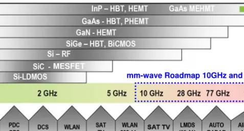
Technology scaling has made CMOS much more attractive for high frequency circuit design. In resent years extensive work has been performed on CMOS RFICs and circuits operating around 60GHz have already been reported [12]. Key characteristics of different materials and a comparison of MMIC technologies are given in Table 1.2 [1]. Currently devices based on SiC (Silicon carbide) and GaN (Gallium nitride) are commercially available and have shown excellent performance particularly for high power amplifier applications. SiC and GaN are also considered promising candidates for future MMICs.
TABLE1.2
KEYCHARACTERISTICSANDCOMPARISON
OFMMICTECHNOLOGIES
Si SiC InP GaAs GaN
Electron mobility At 300oK [cm2/Vs] 1500 700 5400 8500 -2000 1000 Hole mobility At 300oK [cm2/Vs] 450 n.a. 150 400 n.a. Peak electron velocity [107 cm/s] 1.0 2.0 2.0 2.1 2.1 Band gap [eV] 1.1 3.26 1.35 1.42 3.49 Critical break-down field [MV/cm] 0.3 3.0 0.5 0.4 3.0 Thermal conductivity [W/cm.K] 1.5 4.5 0.7 0.5 >1.5 Relative dielectric constant 11.8 10.0 12.5 12.8 9 Substrate resistance [Ωcm] 1-20 1-20 >1000 >1000 >1000 Number of transistors in IC >1 billion <200 <500 <1000 <50
Transistor type MOSFET,
Bipolar, HBT MESFET, HEMT MESFET, HEMT, HBT MESFET, HEMT, HBT MESFET, HEMT Costs: Prototype /mass fabrication High /Low Very high /n.a. High/ Very high Low /High Very high /n.a. Ecological
compatibility Good Good Bad Bad Bad
1.4.1 Speed
The carrier drift velocity gives an insight regarding the speed of device. The carrier drift velocity is a function of applied electric field. Fig 1.2 shows the electron and hole drift velocities for both GaAs and Silicon. The figure indicates that velocity of electrons is higher than that of holes for low and moderate electric fields. Also approximately the peak electron velocity of GaAs is two times higher than that of Silicon. The hole velocity is higher in Silicon as compared to GaAs therefore complementary technologies featuring both type of
1.4 Comparison of MMIC Materials 9
carriers are applied. In contrary to Silicon the difference between electron and hole velocity is significant therefore complementary technologies are not feasible. Another important indicator of speed is mobility that is given by:
dE dv =
µ (1.1)
The mobility µ describes how fast the carrier velocity and the associated current can be varied with respect to an applied electric field E. The time required for carries to reach the maximum frequency is determined by the mobility. Fig. 1.3 shows the mobility of electrons and holes in Silicon and GaAs versus the level of impurities. The plot clearly indicates that compared to GaAs the electron mobility of Silicon based technology is lower. In addition, the mobility of electrons is higher than that of holes, almost 2.5 times higher in Silicon and more than 10 times higher in GaAs. Therefore, for high-speed applications, electrons rather than holes are usually applied as carriers. However, complementary technologies offer certain advantages in the design of analog and mixed-signal circuits, such as current reuse technique can be applied to reduce the overall power consumption. The linearity can also be improved by utilizing complementary technology as indicated by our research (Paper 7).
1.4.2 Integration
GaAs suffers from limited fabrication yield, typical transistor count in GaAs chips is around 1000. Silicon fabrication yield is much better and more than one billion transistors can be implemented on a single chip. Therefore, from SOC (system on chip) point of view Silicon is the only appropriate candidate. As a result, the commercial interest is very much in Silicon RFICs.
1.4.3 Cost
In today’s consumer market there is a strong competition. Therefore, low-cost is the prime goal of IC manufacturers in order to capture the market. Usually, GaAs based technology has lower fixed cost than Silicon based technologies since less processing steps are required [1]. Hence, low volume prototyping costs for GaAs technology is relatively small. The fixed costs are mainly determined by the costs of lithographic masks. However, in mass fabrication, costs can be scaled down more significant for Silicon based technologies due to low variable fabrication cost per IC. Silicon material, which is based on quartz sand, is quite cheap. Therefore, for Silicon based technologies, lower material cost, large wafer size and high yield are the key factors that keep the mass fabrication cost low. Table 1.3 shows the comparison of IC fabrication costs for prototyping and mass fabrication for both technologies excluding the testing and packaging costs [1].
1.4 Comparison of MMIC Materials 11
TABLE1.3
APPROXIMATEICFABRICATIONCOSTS
Prototyping cost (MPW) Mass fabrication (100 wafer) Technology Run cost (€) 1mm 2 IC cost (€) 1mm 2 IC (€) 0.2µm GaAs PHEMT fT = 80GHz 12,000 80 < 1.0 90nm CMOS fT = 110GHz 50,000 330 < 0.1 MPW: Multi Project Wafer, numbers estimated in 2006
1.4.4 Output Power
The speed of CMOS technology is achieved by aggressively downscaling of dimensions. As a consequence, at lower dimensions, the voltages have to be scaled as well to keep the electric field below a critical value. Hence, a major drawback of nanometric CMOS technology is the decrease of maximum possible RF output power.
III/V based technologies do not have to be scaled as aggressively as the Silicon counterparts due to the advantage in terms of speed. Therefore, generally, the supply voltage and associated RF output power is larger. Due to this advantage, mostly GaAs and InP based power amplifier ICs are still used in mobile phones [13].
SiC and GaN based power amplifiers are superior for high power applications as they can handle very high electric fields due to their large band-gap. In addition, their superior thermal conductivity is a big advantage.
1.4.5 Ecologic Compatibility
Considering the recycling or disposal of IC trash, the Silicon based technologies are compatible with environment, since it is based on the natural material quartz sand. Alternatively, GaAs and InP based ICs contains very poisonous materials like arsine and they are not directly compatible with the environment.
1.5 Future Trends and Challenges
Silicon CMOS technology is the leading technology and plays the most important role of today’s IC market. The major reasons are low cost in mass fabrication and the excellent ability for highest level of integration. Reduced supply voltage with technology scaling is one drawback for analog circuit designers. As a consequence the analog circuit design in nanometric CMOS technology is challenging. Fig 1.4 shows an application spectrum and semiconductor devices likely to be used in that frequency range today [11]. Silicon technologies are gradually taking over the RFIC commercial market share from their counterparts due to low-cost chipsets. However, for Military and Space applications where extremely high frequency operation is required, GaAs and InP based devices will continue playing their dominant role. Due to the availability of high resistivity substrate in III/V based technologies, the passive components in these technologies offer much better performance. Therefore, they are suitable choice for extremely high frequency circuits. Fig 1.5
shows the operating frequency of GaAs and InP based device [13]. Limited fabrication yield of III/V based technologies is a major drawback. Hence, from SOC point of view CMOS is the only appropriate candidate. The future wireless marker interest is in CMOS as it provides the possibility to develop and mass-produce low cost chipsets. Radio transceivers for WLAN and GSM applications based on CMOS exclusively have already been reported [14,15].
Figure 1.4 Application spectrum and semiconductor devices likely to be used today
MESFET
1.6 Motivation and Scope of Thesis 13 0 20 40 60 80 100 120 140 160 180 FREQUENCY (GHz) ED02AH: PHEMT D01PH: PHEMT POWER DH15IB: InP DHBT D01MH: 130nm MHEMT
E01MH: 100nm E MODE MHEMT D007IH: 70nm E/D MODE MHEMT
1.6 Motivation and Scope of Thesis
The wireless market is growing at a fast rate; consequently, the RFIC market will continue its rapid growth. The main markets for RFICs involve wireless phones, network, positioning and sensors. There is a growing trend to merge several applications into one device. Therefore, there is a need for reconfigurable circuits. Advantages of reconfigurability are lower overall costs, smaller system size and high market potential.
Two concepts have been investigated in this thesis. The initial part presents the feasibility of a flexible and programmable circuit (PROMFA) that can be utilized for multifunctional systems operating at microwave frequencies. Design details and PROMFA implementation is presented in Paper 1. This concept is based on an array of generic cells, which consists of a matrix of analog building blocks that can be dynamically reconfigured. Either each matrix element can be programmed independently or several elements can be programmed collectively
to achieve a specific function.The PROMFA circuit can therefore realize more
complex functions, such as filters or oscillators. Realization of a flexible RF circuit based on generic cells is a new concept. In order to validate the idea, a test chip has been fabricated in a 0.2µm GaAs process, ED02AH from
OMMICTM. Simulated and measured results are presented along with some key
applications like implementation of a widely tunable band pass filter and an active corporate feed network. Paper 2 addresses the CMOS implementation of PROMFA concept. A test chip has been implemented in a standard 90nm
CMOS technology process. A cell topology with low noise amplifiers have been utilized for this implementation. The test chip demonstrates that with dynamic reconfiguration the same circuit can perform various functions such as tunable oscillator, tunable band pass filter and a low noise amplifier. Chip measurement results indicate a good performance in all three configurations.
The later part of the thesis covers the design and implementation of broadband circuits for multistandard terminals such as software defined radio (SDR). One of the key components in the design of a flexible radio is low noise amplifier (LNA). Considering a multimode and multiband radio front-end, the LNA must provide adequate performance within a large frequency band. Optimization of LNA performance for a single frequency band is not suitable for this application. Narrowband tunable LNAs and wideband highly linear LNAs have been investigated. Paper 3 and Paper 4 presents the design and implementation of a dual band tunable LNA. For the optimization of this LNA a self-tuning technique has also been proposed. A dual band tunable LNA MMIC has been fabricated in 0.2µm GaAs process. Paper 5 presents the design of novel highly linear current mode LNAs that can be used for wideband RF front-ends for multistandard applications. Technology process for this circuit is 90nm CMOS. Paper 6 and Paper 7 covers the design and implementation of wideband RF front-ends. Two test circuits have been implemented utilizing both active and passive mixer configurations. Paper 6 presents a 0.5-6GHz low gain RF front-end for low-IF over-sampling receivers with an active mixer configuration. Paper 7 presents a 6.2mW, highly linear, wideband RF front-end for multistandard receivers. The proposed front-end makes use of a highly linear LNA followed by a passive mixer. The front-end can also withstand large blockers. Simulation and chip measurement results are presented.
1.7 References
[1]. Frank Ellinger, Radio Frequency Integrated circuits and Technologies, Springer, 2007.
[2]. A. Van Dormael, “The French Transistor,” IEEE Conference on the history of Electronics, June 2004.
[3]. B. Stackhousel, B. Cherkauerl, M. Gowan, P. Gronowski, et al., “A
65nm 2 Billion-Transistor Quad-Core Itanium® Processor,” ISSCC 2008.
[4]. http://www.intel.com
1.7 References 15
[6]. C. H. Doan, S. Emami, D. A. Sobel, et al., “Design consideration for 60GHz CMOS radios,” IEEE Communication Magazine, pp. 132-140, December 2004.
[7]. I.D. Robertson, MMIC Design, IEE, 1995.
[8]. H. Wang, K. L. Tan, T. N. Ton, G. S. Dow, P. H. Liu, D. C. Streit, J. Berenz, M. W. Pospieszalski and S. K. Pan, “A high gain low noise 110GHz monolithic two-stage amplifier,” IEEE Int. Microwave Symp. Dig., pp. 783-785, June 1993.
[9]. H. Wang, G. I. Ng, R. Lai, Y. Hwang, D. C. W. Lo, R. Dia, A. Freudenthal, T. Block, “Fully passivated W-band InAIAs/lnGaAs/lnP monolithic low noise amplifiers,” Microwaves, Antennas and Propagation, IEE Proceedings, vol. 143, Issue 5, pp. 361-366, October 1996.
[10]. A. Bessemoulin, P. Fellon, J. Gruenenpuett, H. Massler, W. Reinert, E. Kohn, and A. Tessmann, “High Gain 110-GHz Low Noise Amplifier MMICs using 120-nm Metamorphic HEMTs and Coplanar
Waveguides,” 13th GAAS Symposium-Paris, pp. 77-80, 2005.
[11]. ITRS, http://public.itrs.net
[12]. R. Razavi, “A 60GHz CMOS frontend,” IEEE Journal of Solid State Circuits, vol. 41, no. 1, pp. 17-21, Janaury 2006.
[13]. OMMIC, http://www.ommic.com.
[14]. A. A. Abidi, “RF CMOS comes of age,” IEEE Journal of Solid State Circuits, vol. 39, no. 4, pp. 549-561, April 2004.
[15]. K. Muhammad, Y. C. Ho, T. Mayhugh, C. M. Hung, T. Jung, I. Elahi, C. Lin, I. Deng, C. Fernando, et al., “Discrete Time Quad-Band GSM/GPRS Receiver in a 90nm Digital CMOS Process,” CICC 2005, pp. 809-812, 2005.
Chapter 2
Radio Receiver Architectures
The main function of a receiver front-end is to receive the desired signal in the presence of undesired interferers (usually called blockers) and noise. Depending upon the scenario the received signal may be very weak if the transmitter is far away while at the same time the interferes may be quite strong. Detection of wanted signal in the presence of strong interferers is a challenging job. In addition to this, the wanted signal may also vary in strength due to different scenarios. Therefore, a wide dynamic range is also required. The key design specifications of a radio receiver include sensitivity, selectivity, blocker immunity, power consumption and most important for commercial market the cost. Considering a multimode and multiband radio receiver the front-end should provide the capability to operate the radio in multiple bands for various standards. The provision of GPS, WLAN along with multiband cellular operation to a single mobile phone is a typical commercial example. It is also necessary to limit the additional hardware, particularly; filters, resonators, oscillators, and frequency synthesizers. Therefore, design of a flexible RF front-end under these stringent requirements is challenging.
The initial part of this chapter provides an overview of traditional radio receiver architectures while the later part provides a discussion on flexible receiver architectures.
ANT
RF Filter LNA Image Reject Filter Mixer Channel Select Filter VCO ADC DSP ωRF ωLO ωIF
2.1 Super-Heterodyne Receiver
In 1918, Armstrong proposed the super-heterodyne receiver architecture. Most modern receivers still use similar approach for frequency downconversion with some refinements. The major advantages of a super-heterodyne receiver are its high sensitivity, excellent selectivity and good image rejection. Fig. 2.1 shows the block diagram of a classical super-heterodyne receiver. The received signal from the antenna is filtered by RF band pass filter, amplified by a low noise amplifier. The image frequency is filtered by an image reject filter and the signal is downconverted to a fixed intermediate frequency IF by means of a mixer. The channel select filter selects the desired channel and finally the wanted signal is digitized by an ADC followed by digital demodulation in DSP. Considering the Image problem, a large IF frequency is favorable to relax the requirements for the image rejection filter. A low IF on the other hand relaxes the channel filter requirement. Therefore, the choice of IF is a tradeoff between receiver selectivity and Image rejection. However, this tradeoff can be mitigated by using the dual super-heterodyne architecture [1]. Fig. 2.2 shows this architecture where two different IF frequencies are used. Image rejection is carried out at high IF while the channel selection is accomplished at low IF. Hence, the requirements of both filters can be relaxed simultaneously. For the first VCO, a constant frequency can be used and the frequency tuning is performed by the second VCO that operates at lower frequency. This architecture provides excellent selectivity along with good image rejection.
The major drawback of super-heterodyne receiver is its incompatibility with on chip implementation. Since high Q filters are required for image rejection, typically external SAW (Surface Acoustic Wave) filters are used as on chip implementation of such high Q filters is not feasible. Therefore, a single chip
2.2 Homodyne Receiver 19 RF Filter ANT Image Reject Filter Mixer Mixer Channel Select Filter LNA VCO1 VCO2 ADC DSP ωLO2 ωLO1 ωIF2 ωIF1 ωIF1 >ωIF2
solution with this architecture is rather difficult to build also the receiver with off-chip components like the external filters consume relatively high power [2].
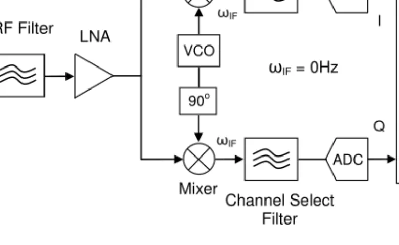
2.2 Homodyne Receiver
In a homodyne receiver the RF signal is directly downconverted to zero-IF frequency [3,4]. It is also called zero-IF or direct conversion receiver. Fig. 2.3 shows the architecture of a homodyne receiver. This architecture dose not require an external high Q image reject filter. Also, the channel select filter can be a simple low pass filter. Therefore, fully integrated on-chip solution is feasible. Since IF frequency is zero, the sidebands allocated around the carrier frequency are translated to DC (0 Hz). For sophisticated frequency and phase modulation schemes, the information of both sidebands can be different, therefore, after conversion around DC, these sidebands can not be separated [5]. This can be prevented by using quadrature mixing with in-phase (I) and quadrature (Q) signals as illustrated in Fig. 2.3. Hartley and Weaver image reject techniques are most widely used. Both techniques are based on the idea of producing two paths having the same polarity for the desired signal, and the opposite polarity for the image signal. Finally, the combination of two paths recovers the desired signal and cancels the image signal [6]. The homodyne receiver shown in Fig 2.3 incorporates the Hartley image reject technique.
The homodyne receiver also has some disadvantages. Since the RF carrier and the local oscillator are at the same frequency, therefore, LO leakage to the mixer input can lead to self mixing resulting in a time-varying DC offset at the output of the mixer. This DC offset not only corrupts the wanted signal but also lead to a saturation of the following stages. As a consequence, the upper boundary of the dynamic range is significantly degraded. To avoid this problem DC offset cancellation circuits are used.
RF Filter ANT Mixer Channel Select Filter LNA VCO ADC Q ωIF ADC DSP ωIF 90o Channel Select Filter Mixer I ωIF = 0Hz
The 1/f noise becomes significant at low frequencies. As the downconverted signal is around DC, therefore, 1/f noise becomes a problem and the wanted signal badly suffers. As a result, the lower limit of the dynamic range is degraded. Some techniques have been proposed to solve this problem [7,8].
The homodyne receiver is also sensitive to I/Q mismatch. The gain and phase errors between I and Q paths can severely degrade the image rejection. However, these errors are not considered significant as they can be corrected in the digital domain.
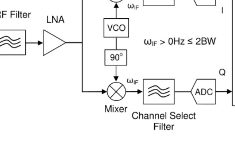
2.3 Low IF Receiver
Low IF receiver is a compromise between the heterodyne and super-heterodyne and it combines the advantages of both receivers. Fig. 2.4 shows the block diagram of a low IF receiver. Typically, the IF frequency is chosen to be one or two times the channel bandwidth [9]. Due to low IF frequency the channel filtering is relatively simple and all relevant filters can be implemented on-chip. The advantage of low IF receiver is that there is no problem of DC offset, LO leakage and 1/f noise. The image rejection can be performed by either Hartley or by Weaver quadrature downconversion technique.
Like homodyne receiver, the low IF receiver is also sensitive to I/Q mismatch. For fully integrated solutions with symmetrical designs, the gain and phase errors between I and Q paths are usually small. It is also possible to correct these errors in the digital domain therefore, practical implementations typically exhibit image rejection of more than 30dB [10].
2.4 Flexible Receiver Front-end 21 RF Filter ANT Mixer Channel Select Filter LNA VCO ADC Q ωIF ADC DSP ωIF 90o Channel Select Filter Mixer I ωIF > 0Hz ≤2BW ANT LNA ADC DSP
2.4 Flexible Receiver Front-end
The choice of radio receiver architecture strongly depends on the system specifications and application. Digitalized radio receivers can offer more flexibility due to their powerful signal processing capability. With the availability of high performance ADCs the analog to digital conversion can be performed directly at RF frequency. Fig. 2.5 illustrates the architecture of a digitalized radio receiver that performs downconversion and demodulation in digital domain [11]. With this topology, the demodulation of multiple channels can be performed simultaneously by means of parallel DSP blocks. Therefore, a multistandard radio that can be reconfigured by software can be realized by this architecture. However, in practice, the ADC limits the dynamic range of such a receiver. Typically, ADCs for this high-speed operation consumes much more power therefore, this solution is not feasible for portable devices.
Figure 2.4 Low IF Receiver
Another alternate approach is RF-Sampling Receiver. Various topologies have already been proposed [12-15]. The direct RF-Sampling technique provides great flexibility in the implementation of a reconfigurable radio [14].
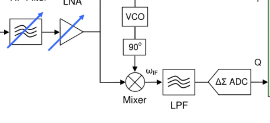
As discussed in the previous section, the homodyne and low IF topologies are best suited for on-chip implementations. With multiband LNA and programmable filters, these architectures can be very flexible and hence they are popular candidates for multimode receivers. We have investigated the feasibility of a filter-less radio receiver front-end [16]. The channel selection in proposed architecture (Fig. 2.6) is performed digitally. The baseband signal is band limited by simple on-chip second order LPF that also helps in reducing the level of out of band blocker signals. The desired baseband signal (including adjacent channel blockers) is noise shaped by over-sampled ∆Σ-ADC. Both low pass and band pass ∆Σ-ADC topologies are feasible for this architecture. With this architecture, a relatively large dynamic range can be achieved. The RF filter requirements can also be relaxed and even it can be avoided if the following stages are highly linear. In operation, the proposed architecture is similar to [17] where a pseudodirect conversion topology is used for a multimode cellular radio. Like [17] it can either operate as a low IF receiver for narrowband standards such as GSM, EDGE etc. or as a zero IF receiver for wideband standards like WCDMA. Therefore, the proposed architecture offers a flexible on-chip radio receiver solution. However, the linearity requirements are extremely tough and the lower limit of the dynamic range may also degrade due to the thermal noise (KT/C) of the sampling capacitor at the input of ADC.
Figure 2.6 Flexible Receiver Frontend for Multistandard Radio
RF Filter ANT Mixer LPF LNA VCO Q ωIF DSP ωIF 90o Mixer I ∆Σ ADC ∆Σ ADC LPF
2.5 References 23
2.5 References
[1]. X. Li and M. Ismail, Multi-standard CMOS Wireless Receivers; Analysis and design, Kluwer, 2002.
[2]. A. Abidi, “Direct-Conversion Radio Transceivers for Digital
Communications,” IEEE Journal of Solid State Circuits, vol. 30, no. 2, pp. 1399-1409, February 1995.
[3]. P. Zhang, T. Nguyen, C. Lam et al., “A 5GHz direct conversion CMOS transceiver,” IEEE Journal of Solid State Circuits, vol. 38, no. 12, pp. 2232-2238, December 2003.
[4]. B. Razavi, “Design considerations for direct conversion receivers,” IEEE Transactions on Circuits and Systems II: Analog and Digital Signal Processing, vol. 44, no. 6, pp.428-435, June 1997.
[5]. J. Crols, M. Steyaert, CMOS Wireless Transceiver Design, Kluwer, 1997.
[6]. Frank Ellinger, Radio Frequency Integrated circuits and Technologies, Springer, 2007.
[7]. H. Darabi, J. Chiu, “A Noise Cancellation Technique in Active RF-CMOS Mixers,” IEEE Journal of Solid State Circuits, vol. 40, no. 12, pp. 2628-2632, December 2005.
[8]. R. S. Pullela, T. Sowlati and D. Rozenblit, “Low Flicker Noise Quadrature Mixer Topology,” ISSCC 2006, pp. 466-467, 2006.
[9]. S. Mirabbasi, K. Martin, “Classical and Modern Receiver Architectures,” IEEE Communications Magazine, vol. 38, no. 11, pp. 132-139, November 2000.
[10]. M. Windisch, G. Fettweis, “Adaptive I/Q imbalance compensation in low-IF transmitter architectures,” IEEE Vehicular Technology Conference, vol. 3, pp. 2096-2100, September 2004.
[11]. T. Hentschel, M. Henker, G. Fettweis, “The Digital Frontend of Software Radio Terminal,” IEEE Personal Communications, vol. 6, no. 4, pp. 40-46, August 1999.
[12]. D. Jakonis, Direct RF-Sampling Receivers for Wireless Systems in CMOS Technology, PhD Thesis, Linköping University, Department of Electrical Engineering, SE 581 83 Linköping, Sweden, 2004.
[13]. S. Andersson, Multiband LNA Design and RF-Sampling Front-Ends for Flexible Wireless Receivers, PhD Thesis, Linköping University,
Department of Electrical Engineering, SE 581 83 Linköping, Sweden, 2006.
[14]. S. Andersson, J. Konopacki, J. Dabrowski and C. Svensson, “SC Filter for RF Sampling and Downconversion with Wideband Image Rejection,” Journal of Analog Integrated Circuits and Signal, Springer, Special Issue: MIXDES 2005, Published online June 2006.
[15]. K. Muhammad, R. B. Bogdan, and D. Leipold, “Digital RF Processing: Toward Low-Cost Reconfigurable Radios,” IEEE Communications Magazine, pp. 105-113, August 2005.
[16]. S. Ahmad, N. Ahsan, A. Blad, R. Ramzan, T. Sundström, H. Johansson, J. Dabrowski, and C. Svensson, “Feasibility of Filter-less RF Receiver Front end,” Giga Hertz Symposiun 2008, Göteborg, Sweden, March 2008.
[17]. J. Groe, “A Multimode Cellular Radio,” IEEE Transactions on Circuits and Systems-II: Express Briefs, vol. 55, no. 3, pp. 269-273, March 2008.
Chapter 3
Programmable Microwave Function
Array (PROMFA)
Most of today’s microwave circuits are designed for specific function and special need. This conventional way of designing these high frequency circuits limits their ability to adapt to new demands and consequently it limits the flexibility of the whole system. There is a growing trend to have flexible and reconfigurable circuits. Circuits that can be digitally programmed to achieve various functions based on specific needs. With the recent advances in technology, these demands can now be met. Some efforts have been made with evolvable hardware, such as [1], where a mixer is automatically adjusted for best performance. The idea of having flexible RF systems with reconfigurable circuit blocks is becoming more and more popular. Various solutions have already been proposed for example: a flexible VCO based on tunable active inductor in [2], and a reconfigurable band pass filter for multifunctional systems in [3]. Some approaches of reconfiguration are based on MEMS (Micro-electromechanical systems), such as a reconfigurable power amplifier and a flexible low noise amplifier reported in [4-5].
PROMFA cell Digital Control PROMFA cell PROMFA cell PROMFA cell
FPAA (Field Programmable Analog Array) is another approach for the implementation of reconfigurable circuits [6-11]. In this approach, two dimensional array of CABs (Configurable Analog Blocks) is utilized for the implementation of flexible filters. These CABs include digitally configurable transconductance amplifiers connected through a hexagonal interconnect network. Various filter configurations can be implemented by means of reconfigurable signal routing inside the array.
This chapter provides the details of PROMFA (Programmable Microwave Function Array) circuit which consists of a matrix of analog building blocks that can be dynamically reconfigured [12,13]. Either each matrix element can be programmed independently or several elements can be programmed collectively to achieve a specific function. The PROMFA circuit can therefore realize more complex functions, such as filters or oscillators.
3.1 PROMFA Concept
The concept is based on an array of generic cells. The idea is similar to a FPAA approach, but for analog signals in the microwave region. A block schematic overview of such a system is illustrated in Fig. 3.1. Here the analog building blocks (PROMFA cells) are connected together, and to control the behavior of each analog cell digital control logic is placed between them. The individual PROMFA cells can be configured in a number of ways, for example as an amplifier, power splitter, power combiner, router etc. The array can therefore realize more complex functions, such as filters or oscillators. The PROMFA system utilizes a 2D mesh network topology which is also common routing topology used by digital network routers.
3.2 Single PROMFA Cell 27
3.2 Single PROMFA Cell
The PROMFA cell has several different possibilities to connect the four different ports to each other. Because of the symmetry of the cell, any port can be either an input or an output. The signal path can be either of pass-transistor type (simple switch) or amplifying depending on the biasing of the cell. This gives a number of different configurations. A single cell is described in the block schematic in Fig. 3.2. At each of the four ports, a transistor switch is placed to open or close the port. The transistor size is adjusted to achieve good matching both to other cells and to a 50 ohm system. The eight grey blocks are common source amplifier stages with transistor arrays. The white blocks are switching transistors, used for bi-directional signal paths. By activating different stages, the different functions can be realized [13].
Figure 3.2 Block diagram of a single PROMFA cell
(a) Chip photo (b) Test fixture photo Figure 3.3 PROMFA chip photographs
Fig. 3.4 illustrates the PROMFA sub cell that includes a bi-directional amplifier stage and a bypass (pass-transistor switch). The input signal can be routed either through a direct path (pass-transistor) or through bi-directional amplifier stage. The bi-directional amplifier stage allows the possibility to amplify signal in both directions depending on requirement.
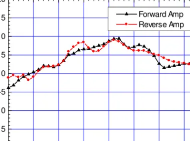
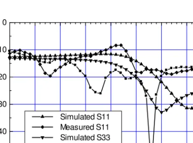
The circuit is designed in such a way that it has symmetry that makes it a reciprocal network. Fig. 3.5 shows the measured gain of forward and reverse amplifier. This plot indicates the reciprocity of PROMFA cell. The forward and reverse amplifiers are not allowed to operate concurrently and based on requirement one of them is switched on at a time. Fig. 3.6 shows the comparison of simulated and measured results for amplifier gain and isolation. Fig. 3.7 shows the variation in input and output reflection coefficients versus frequency. The amplifier transistor array also provides three possibilities of phases. The delay through an amplifier corresponds to a phase shift Ф that can be expressed as:
Φ = +π 2πn=ω τc =2π τfc (3.1)
Where
τ
is the amplifier time constant and given by:
τ
∝CgmL (3.2)
(a) Block diagram (b) Transistor array with bypass switch Figure 3.4 Illustration of PROMFA sub cell
3.2 Single PROMFA Cell 29 4.0 4.5 5.0 5.5 6.0 6.5 7.0 7.5 8.0 -20 -15 -10 -5 0 5 10 15 20 Forward Amp Reverse Amp M E A S U R E D G A IN ( d B ) FREQUENCY (GHz)
It means that
τ
can be controlled by the variation of gm. In addition, gm is dependent on transistor width:gm∝WT (3.3)
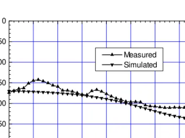
Therefore, different delays can be achieved by changing the width of transistor. The control transistors are used to get three phase possibilities Ф1, Ф2 and Ф3. Fig. 3.8 shows the relative phase shift of transistor array amplifier with three possibilities. Fig. 3.9 shows the comparison of measured and simulated phase response for phase possibility Ф3. A single PROMFA sub cell only provides three possibilities. The results indicate that the relative phase shift has a reasonable flat response. The concept can be extended to get the other phase possibilities by connecting additional PROMFA cells.
Each PROMFA subcell requires seven control lines that includes three control lines for each transistor array and one for bypass. Four control lines are also needed for the port switches. Therefore, in total, 32 control lines are needed for a single PROMFA cell. For the first prototype, we have used four off-chip serial to parallel (S/P) converters each controlling one subcell. The chip is controlled through four serial lines using a computer based data acquisition card and Lab-View© software.
4.0 4.5 5.0 5.5 6.0 6.5 7.0 7.5 8.0 -80 -60 -40 -20 0 20 Simulated S31 Measured S31 Simulated S13 Measured S13 S 3 1 /S 1 3 ( d B ) FREQUENCY (GHz) 4.0 4.5 5.0 5.5 6.0 6.5 7.0 7.5 8.0 -50 -40 -30 -20 -10 0 Simulated S11 Measured S11 Simulated S33 Measured S33 S 1 1 /S 3 3 ( d B ) FREQUENCY (GHz)
Figure 3.6 Measured and simulated response of PROMFA amplifier (Gain S31, Isolation S13)
3.2 Single PROMFA Cell 31 4.0 4.5 5.0 5.5 6.0 6.5 7.0 7.5 8.0 -300 -250 -200 -150 -100 RE L A T IV E P H A S E ( DE G RE E S ) FREQUENCY (GHz) Φ1 Φ2 Φ3 4.0 4.5 5.0 5.5 6.0 6.5 7.0 7.5 8.0 -350 -300 -250 -200 -150 -100 -50 0 Measured Simulated R E L A T IV E P H A S E ( D E G R E E S ) FREQUENCY (GHz)
Figure 3.8 Relative phase shift of transistor array amplifier
Input
e
-jωτ Output Amplifier α1 β1 Power splitter Power combiner β2 α2 GA , FA3.3 Tunable Band pass Filter
Active recursive band pass filters are very interesting for microwave applications. A traditional recursive band pass filter is accomplished according to the model in Fig. 3.10. This model is based on positive feedback, where some of the output is fed back to the input through a delay
τ
. The input couplingfactor is denoted by α1 while β1 is the feedback coupling factor. Similarly α2 and β2 are coupling factors of the output power splitter. The amplifier gain and noise figure are denoted by GA and FA respectively. By varying the delay in the feedback loop, a phase shift is accomplished that changes the center frequency of filter [14].
The filter gain can be expressed as:
( )
( )
(
)
2 2 2 1 2 1 2 1 2 1 2 1 cos 2 1 + − = A A A fil G S S G S S G G β β β β ωτ ββ β β α α ω (3.4)where Sβ1and Sβ2are the transmission parameters (loss/gain) of power divider and power splitter path. At filter centre frequency
( )
ωO the gain can beexpressed as:
( )
2 2 1 2 1 2 1 1 − = A A O fil S S G G G β β β β α α ω (3.5)For a lossless and symmetrical power divider/combiner: Sβ1=Sβ2=1 and 2 1 2 1 2 1=α =β =β =
α , hence (3.5) reduces to: