Electrical resistivity and morphology of ultra thin Pt films grown by dc magnetron sputtering on
SiO2
This article has been downloaded from IOPscience. Please scroll down to see the full text article.
2008 J. Phys.: Conf. Ser. 100 082006
(http://iopscience.iop.org/1742-6596/100/8/082006)
Download details:
IP Address: 130.237.43.227
The article was downloaded on 01/03/2011 at 16:22
Please note that terms and conditions apply.
Electrical resistivity and morphology of ultra thin Pt
films grown by dc magnetron sputtering on SiO
2J S Agustsson1, U B Arnalds2, A S Ingason3, K B Gylfason4, K Johnsen1, S Olafsson3 and J T Gudmundsson3,5
1
Mentis Cura, Grandagardi 7, Reykjavik, Iceland 2
Matvice ehf, Dunhaga 3, Reykjavik, Iceland 3
Science Institute, University of Iceland, Reykjavik, Iceland 4
Microsystem Technology Laboratory, School of Electrical Engineering, KTH-Royal Institute of Technology, Stockholm, Sweden
5
Department of Electrical and Computer Engineering, University of Iceland, Reykjavik, Iceland
E-mail: tumi@hi.is
Abstract. Ultra thin platinum films were grown by dc magnetron sputtering on thermally oxidized Si (100) substrates. The electrical resistance of the films was monitored in-situ during growth. The coalescence thickness was determined for various growth temperatures and found to increase from 1.3 nm for films grown at room temperature to 1.8 nm for films grown at 250◦C, while a continuous film was formed at a thickness of 3.9 nm at room temperature and 3.5 nm at 250◦C. The electrical resistivity increases with increased growth temperature, as well as the morphological grain size, and the surface roughness, measured with a scanning tunneling microscope (STM).
1. Introduction
Ultra thin films are an essential part of modern technology such as in device interconnects in microelectronics [1]. As the dimensions of a conductor approach the mean free path of the conducting electrons, size effects limit the electrical conductivity. The electrical resistivity of thin conducting films influences device operating frequency, current, and Joule heating of the device, which in turn can cause electromigration [2]. The reduced electrical conductivity can be attributed to scattering of conduction electrons at the surface of the conducting film [3], interface roughness [4] and grain boundaries [5].
Most metals do not wet insulating surfaces such as glass or silicon [6]. When sufficiently thin, a metal film consists of small isolated islands, which, as more material is deposited, grow and coalesce into larger, but still isolated islands. As growth continues further, these islands coalesce into near equilibrium compact shapes which further develop into a continuous film [7].
In microelectronics, platinum (Pt) is the material of choice for metallic components that are to withstand oxidation. Xu et al. [8] have suggested a two-dimensional growth mechanism for Pt thin films on an a-C surface since the fractional substrate coverage scales linearly with the film thickness. Furthermore, using transmission electron microscopy (TEM) they find that Pt coalesces at 1.0 nm and fully covers the substrate at 4.0 nm thickness. The electrical resistance
of Pt thin films has been monitored in-situ during growth by argon ion–beam sputtering (IBS) [9, 10] and filtered cathodic arc [11]. The morphological and crystallographical grain sizes of Pt films grown by filtered cathodic arc have been investigated by scanning tunneling microscopy (STM) and X-ray diffractometry (XRD) [12]. The crystallographic grain sizes are the grain dimensions embedded in the bulk of the film while the morphological grain sizes are the grain dimensions exposed on the film surface.
Here, we explore the initial growth and subsequent thickness development of Pt thin films grown by dc magnetron sputtering on thermally oxidized silicon (SiO2). We measure the
electrical resistance of the films in–situ during growth at three different growth temperatures and investigate the morphological and crystallographical grain sizes.
2. Experimental apparatus
The Pt thin films were grown in a custom built magnetron sputtering chamber. A turbo molecular pump was used to evacuate the system to 1 × 10⁻⁸ Torr. The sputtering gas was
argon of 99.999% purity and pressure 0.4 mTorr. The Pt target was 50 mm in diameter and of 99.99% purity. The applied power was set to 20 W resulting in a growth rate of 0.025 nm/s. The growth rate was determined by low–angle X–ray reflection measurements with a copper tube (CuKα, wavelength 0.15406 nm) and angular resolution of 0.005◦. The crystallographic grain
size was determined using X-ray diffractometry and the Scherrer equation [13].
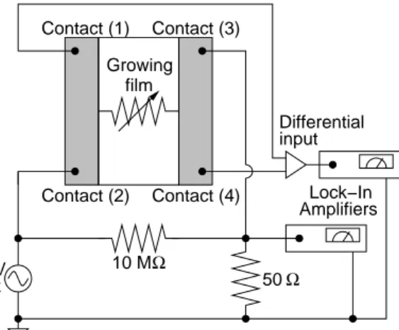
Contact (2) Contact (1) Contact (3) Macor Ceramic Contact (4) pad pad grown Contact Area to be Contact
Figure 1. A schematic of the sample holder. An SiO2 substrate, with two Pt contact pads,
was placed on top of the sample holder. Two electrical probes were connected to each contact pad. Growing input Contact (4) Contact (2) 417 Hz 600 mV 50Ω AmplifiersLock−In 10 MΩ Contact (3) Contact (1) film Differential
Figure 2. The dual lock–in amplifier setup used to measure the electrical resistance of the growing films in–situ. The setup is a standard four point probe measurement.
The substrate is thermally oxidized Si (100) with an oxide thickness of 500 nm. Pt contact pads of size 8.5 mm × 2.8 mm and a thickness greater than 70 nm were formed by optical lithography, dc magnetron sputtering, and a lift-off. The contact pads are separated by 8.5 mm × 3.0 mm uncoated SiO2 area. The substrate holder is made from Macor ceramic to
electrically isolate the four probe tips from each other and from the sample stage. A shadow mask confines the growth to a rectangular area as illustrated in figure 1. The electrical resistance of the growing film was measured with a simplified version of the dual lock-in amplifier setup described by Barnat et al. [14], shown in figure 2. The setup is a standard four point probe electrical resistance measurement, based on measuring both the voltage over the film, directly, and the current passing through the film, indirectly, by monitoring the voltage over a 50 Ω resistor in series with the film, thus eliminating the effect of contact resistance. A function generator (Tabor 8021) was used to generate a 600 mV rms sinusoidal signal at 417 Hz. The
electrical resistance measured in-situ for films grown at three different temperatures. Four films grown to different thicknesses at room temperature were investigated further. Immediately after growth the samples were heated from room temperature up to approximately 450◦C at a rate
of 1◦C/min while their resistance was monitored.
The morphological grain size and surface roughness were measured ex-situ with a scanning tunneling microscope (STM) with an etched tungsten tip. The custom made STM is described elsewhere [15].
3. Results and discussion
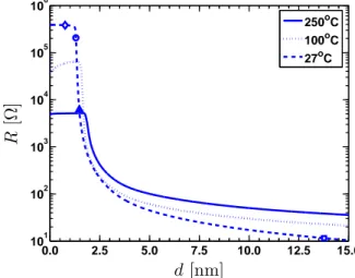
Figure 3 shows the electrical resistance R as a function of nominal film thickness d measured in–situ during growth at three different temperatures. Initially the film is discontinuous as indicated by the high resistance. A coalescence threshold is defined as the thickness where the first conducting link forms across the surface [9]. The electrical resistance decreases rapidly as the film starts coalescing. This occurs at thicknesses of 1.3 nm, 1.6 nm, and 1.8 nm for the films grown at 27, 100, and 250◦C, respectively. The minimum of the calculated curve Rd2
, gives the minimum thickness of a continuous film [9, 10]. This occurs at 3.9 nm, 3.4 nm, and 3.5 nm for the films grown at 27, 100, and 250◦C, respectively. In comparison, Maaroof et al. [10] find
the minimum thickness of Pt films which completely cover the substrate to be 2.30 nm for films grown at 27 – 200◦C and 0.35 nm for films grown at 300◦C and the coalescence thickness to be
0.83 nm, 0.67 nm, and 0.61 nm for films grown at 27, 100, and 200◦C, respectively.
0.0 2.5 5.0 7.5 10.0 12.5 15.0 101 102 103 104 105 106 250oC 100oC 27oC R [Ω ] d [nm]
Figure 3. The electrical resistance, R, as a function of Pt film thickness, d, measured in– situ during growth, for three different growth temperatures. 0 100 200 300 400 500 0.0 0.5 1.0 1.5 d = 14 nm d = 1.4 nm d = 1.2 nm d = 0.8 nm R /R R T T [◦C]
Figure 4. The normalized film electrical resistance R/RRT versus temperature for a
film grown at room temperature. The symbols correspond to the symbols marking thickness and resistance shown in figure 3. As the film thickness increases, its electrical resistance decreases until the room temperature resistivity reaches values close to 3.5 × ρ0, 4.6 × ρ0, and 5.0 × ρ0 for the films grown at 27, 100,
and 250◦C, respectively. The bulk resistivity of Pt is ρ0 = 10.6 µΩ cm at room temperature.
Higher growth temperature results in higher film resistance. The symbols on the 27◦C curve in
figure 3 indicate the resistance and film thicknesses values chosen to investigate the resistance dependence on temperature in figure 4. The thinnest films show the characteristic behavior of thermally induced conductance: decreased resistance with increased temperature as expected in insulating materials. As the films become thicker the thermally induced conductance is masked
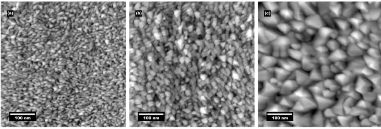
Figure 5. STM images of the surface of 85 nm thick Pt films grown on SiO2 at (a) 27◦C, (b)
100◦C, and (c) 250◦C, respectively.
by metallic conductance. The resistance of the thickest film indicates metallic conduction, that is increased resistance with increased temperature.
Figure 5 shows STM images of the surface of 85 nm thick Pt films grown at three different temperatures. The morphological grain size of these films was evaluated 21, 24, and 52 nm and the RMS surface roughness was estimated 1.6, 1.8, and 2.7 nm for the films grown at 27, 100, and 250◦C, respectively. The crystallographical grain size for 85 nm thick films was determined
30, 33, and 40 nm for the films grown at 27, 100, and 250◦C, respectively.
4. Conclusion
The electrical resistivity of ultra thin Pt films was explored during growth. Higher growth temperature leads to increased film resistivity. This could be partially related to increased surface roughness with increased growth temperature. However, the morphological grain size and the crystallographical grain size increase with increased growth temperature, which should result in lower electrical resistivity.
Acknowledgments
This work was partially supported by the Icelandic Research Fund, the Steinmaur Foundation and the University of Iceland Research Fund.
References
[1] Steinhoegl W, Schindler G, Engelhardt M 2005 Semicond. Int. 28 (May) 34 [2] Banerjee K, Mehrotra A 2001 IEEE Circuits Devices Mag. 17 16
[3] Sondheimer E H 1952 Adv. Phys. 1 1 [4] Namba Y 1970 Jap. J. Appl. Phys. 9 1326
[5] Mayadas A F, Shatzkes M. 1970 Phys. Rev. B 1 1382 [6] Eustathopoulos N, Drevet B 1994 J. Physique III 4 1865
[7] Yu X, Duxbury P M, Jeffers G, Dubson M A 1991 Phys. Rev. B 44 13163 [8] Xu S, Evans B L, Flynn D I, En C 1994 Thin Solid Films 238 54
[9] Rycroft I M, Evans B L 1996 Thin Solid Films 290-291 283 [10] Maaroof A I, Evans B L 1994 J. Appl. Phys. 76 1047
[11] Salvadori M C, Vaz A R, Farias R J C, Cattani M 2004 Surf. Rev. Lett. 11 223
[12] Salvadori M C, Melo L L, Vaz A R, Wiederkehr R S, Teixeir F S, Cattani M 2006 Surf. Coat. Techn. 200 2965
[13] Cullity B D 1978 Elements of X-Ray Diffraction, 2nd ed. (Reading, Massachusetts: Addison-Wesley) [14] Barnat E V, Nagakura D, Lu TM 2003 Rev. Sci. Instr. 74 3385
[15] Arnalds U B, Bjarnason E H, Jonsson K, Olafsson S 2006 Appl. Surf. Sci. 252 5485