Hardware Platform for Mobile Adaptable
Surveillance System for Critical Areas
Tamene Tujuba
Master Thesis 2011
Electrical Engineering
Hardware Platform for Mobile Adaptable
Surveillance System for Critical Areas
(MASURCA)
Tamene Tujuba
This thesis work has been carried out at Saab Training Systems AB and Jönköping University School of Engineering in Jönköping in the subject area Electrical Engineering. The work is part of the two – year Master degree program with the specialization in Embedded Systems. The author takes full responsibility for opinions, conclusions and findings presented.
Supervisor (Industry): Michel Chedid, Saab Training Systems AB
Supervisor (JTH): Alf Johansson
Examiner JTH): Professor Shashi Kumar
___________________________________________
Acknowledgement
In the name of the Almighty God who has always helped me with potential knowledge and success.
I would like to express my deepest appreciation and thanks to Saab Training Systems AB for the opportunity.
I am thankful to my supervisor Michel Chedid, for his continuous helps and guidance during the entire design work.
I would like to extend my personal gratitude to Mikael for helping and assisting me during the design work.
I would like to express my special thanks to my supervisor Alf Johansson, for his constructive ideas and guidance during the entire work.
I am especially thankful to my parents, and my girlfriend Mekdes Shewareged, who had always provided me the courage, strength, best wishes and financial support during my whole career.
Abstract
Smart Environment is built with the help of embedded system that can give an access to the environment in which it is placed. The embedded systems are electronic systems constituting electronic devices which are specially built to facilitate certain processes such as the human interaction with an environment. These systems play a vital role in an electronic application systems such as medical diagnosis, geological investigation, surveillances, cash records, play stations and etc. The Mobile Adaptable Surveillance System for Critical Areas (MASURCA) is an embedded system wireless sensor network application system that embodies both the hardware (node) and software. In this thesis project, Development of Hardware Platform for Mobile Adaptable Surveillance System for Critical Areas, the design and development of the hardware platform for the system is built. The project deals with building the smart system comprising of radio frequency (RF) radio, global positioning system (GPS) sensor module, Accelerometer, Temperature sensor, and Ultrasonic sensor.
The design focuses on designing the power supply stage from a single AA battery in such a way that the entire connected components and sensors get a required supply source with best possible extended battery life. The design of power supply stage includes EMC, signal integrity, thermal and efficiency design considerations, and prototyping and testing of the power supply stage.
First the sensors and the necessary design components are selected with more emphasis on their power/energy consumption, size of footprint and signal output (I2C-bus protocol interface capability). Then the system schematic will be designed and simulated for signal integrity and design rule using the Mentor Graphics design entry Dxdesigner and hyperlynx Analog simulator. The designed schematic is also packaged and the part is listed and the bill of material is generated so as to be able to annotate to the PCB layout and later component placement.
Likewise, the PCB layout is designed according to the Saab Training Systems AB’s standards, regulatory guidelines and standards, and the MASURCA main node system specific requirements. The project will also design and provide the mechanical enclosure kit and software development kit for the MASURCA main node hardware platform. Finally testing and evaluation of the system is done to make the hardware ready for the application implementation.
Sammanfattning
I detta examensarbete, ”Mobile Adaptable Surveillance System for Critical Areas (MASURCA)” utvecklas en hårdvaruplattform för ett mobilt, anpassningsbart övervakningssystem för kritiska områden. Projektet handlar om att bygga smarta system bestående av mikrodator, radiokrets (RF), GPS-modul (Global Positioning System), accelerometer, temperaturgivare och ultraljudsgivare.
Konstruktionsarbetet har fokuserats på att konstruera ett strömförsörjningssteg så att man från ett Li-ion AA-batteri klarar att ansluta komponenter och sensorer och få bästa möjliga batteritid. Konstruktionen av strömförsörjningssteget omfattar också EMC, signalintegritet, termisk och design och prototypframtagning och testning av strömförsörjningssteget.
Först valdes komponenter med speciellt fokus på energiförbrukning, fysisk storlek och elektriska gränssnitt. Sedan utformades scheman och konstruktionen simulerades för att verifiera funktion och signalintegritet med hjälp av Mentor Graphics Dxdesigner och Hyperlynx analog simulator.
Likaså är PCB-layouten utformad i enlighet med Saab Training Systems AB:s standarder, andra regulatoriska riktlinjer och standarder, och MASURCAs specifika krav. Projektet syftar också på att ta fram ett mekaniskt hölje och ett ”Software Development Kit” för MASURCAs huvudnod. Slutligen gjordes testning och utvärdering av systemet. Hårdvaran färdigställdes så att den kunde implementeras i övriga systemet. Hårdvaran kan arbeta med full funktion från ett enda Lithium-batteri och den förbrukar 150mA vid 3,3V matningsspänning. Sensornodernas lokaliseringsförmåga möjliggörs av den monterade GPS-modulen.
Key Words
Wireless Sensor Networks Location Aware
List of Abbreviations
MASURCA Mobile Adaptable Surveillance Systems for Critical Areas VINNOVA The Swedish Governmental Agency for Innovation
Systems
COTS Commercial-off-the-shelf HW Hardware
EMC Electromagnetic Compatibility EDA Electronic design automation MCU Microcontroller unit
RF Radio frequency PCB Printed circuit board CPU Central processing unit WSN Wireless sensor network Hz Hertz
RAM Read access memory µAMPS Micro Amperes
DPM Dynamic power management OS Operating system
Input dc voltage
MOS Metal oxide semiconductor
EEPROM Electrically erasable programmable read only memory ADC Analog to digital convertor
MOSFET Metal oxide semiconductor field effect transistor SRAM Static random access memory
PWM Pulse width modulation PFM Pulse frequency modulation WLNT Wireless LAN network LQI Link quality indicator
List of Figures
FIGURE 2-1 A TYPICAL WIRELESS SENSOR NODE. 5 FIGURE 2-2 AN EXAMPLE OF SENSOR NETWORK [34]. 8 FIGURE 2-3 THE COMPONENTS OF SENSOR NODE. 11 FIGURE 2-4 A STANDARD DC-DC STEP UP CONVERTER. 19 FIGURE 2-5 A COMMON ARCHITECTURE OF RF TRANSCEIVER. 21 FIGURE 3-1 MASURCA MAIN NODE DESIGN BLOCK. 26 FIGURE 3-2 A BLOCK DIAGRAM OF MASURCA MAIN NODE POWER SUPPLY. 26 FIGURE 3-3 OUTPUT ADJUSTABLE LM3670-ADJ. 28 FIGURE 3-4 AN OVERVIEW OF MASURCA MAIN NODE CONNECTED COMPONENTS. 33
FIGURE 4-1 MASURCA MAIN NODE. 37
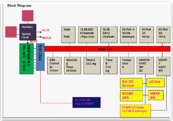
FIGURE 4-2BLOCK DIAGRAM OF MASURCA MAIN NODE COMPONENTS INTERCONNECTION. 38 FIGURE 4-3 MASURCA MAIN NODE PCB CARD. 40 FIGURE7-1FUNCTIONALB LOCK DIAGRAM OF MASURCA MAIN NODE MODULE, COMPONENTS AND
BUSES.
FIGURE 7-2 SCHEMATIC OF THE MASURCA MAIN NODE. 51 FIGURE 7-3 DEVICE MANAGER SHOWING MASURCA (MAIN NODE) INSTALLED AS COM4. 54 FIGURE 7-4 BLOCK DIAGRAM OF THE TI MSP430 MICROCONTROLLER AND ITS CONNECTION TO THE
OTHER PERIPHERALS IN THE MASURCA (MAIN NODE) MODULE. 55 FIGURE 7-5 M10382 RECEIVER DDC/I2C REGISTER LAYOUT. 60 FIGURE 7-6 FLOWCHART FOR RANDOM READ ACCESS. 61 FIGURE 7-7 FLOWCHART FOR WRITING CONFIGURATION COMMANDS. 62
List of Tables
Table 4-1 MASURCA Main Node power rating 34
Table 4-2 MASURCA Main Node slave devices clock speed and I2C address 35
Table 7.1 Typical Operating Conditions of MSP430F1611 46
Table 7.2 Typical Operating Conditions for AT86RF231 49
Table7.3 Recommended operating conditions, DC electrical 51
characteristics and receiver sensitivity for GPS (M10382) Table 7.4 MMA8450 Electrical and I2C interface characteristics 52
Contents
1
Introduction ... 1
1.1 THESIS GOALS AND TASKS ... 1
1.2 BACKGROUND ... 2
1.3 PURPOSE AND DESIGN/RESEARCH QUESTIONS ... 2
1.3.1 Design Questions ... 3
1.4 DELIMITATIONS ... 3
1.5 OUTLINE ... 3
2
Theoretical background ... 4
2.1 WIRELESS SENSOR NETWORKS ... 4
2.2 CHARACTERISTICS ... 5
2.3 SECURITY MONITORING ... 5
2.4 REQUIREMENTS... 7
2.4.1 Challenges in power management... 7
2.5 WIRELESS SENSOR NETWORK NODE ... 10
2.6 HARDWARE FOR WIRELESS SENSOR NETWORK ... 14
2.6.1 General Purpose Commodity based Sensor Nodes ... 16
2.7 POWER SUPPLY ... 17
2.7.1 Battery ... 17
2.7.2 DC-DC Converter ... 18
2.7.3 Wireless Sensor Node Radio Transceiver ... 21
2.8 SENSORS ... 23
2.8.1 Global Positioning System (GPS) ... 23
2.8.2 Acceleration Sensor ... 24
3
MASURCA main node: Design and Implementation ... 25
3.1 DESIGN ... 25
3.2 IMPLEMENTATION ... 28
3.2.1 Power Supply ... 28
3.2.2 I2C Bus Level Translator ... 32
3.2.3 Sensors ... 32
3.2.4 Printed Circuit Board ... 34
3.2.5 Application Programming Interface ... 34
4
Design results and analysis ... 37
5
Conclusions and future work ... 41
5.1 CONCLUSIONS ... 41
5.2 FUTURE WORK... 42
6
References ... 43
1
Introduction
1.1 Thesis Goals and Tasks
The project MASURCA is a project supported by VINNOVA (The Swedish Governmental Agency for Innovation Systems) and MSB (Swedish Civil Contingencies Agency), and is owned by Saab Training Systems AB. It targets developing a wireless sensor network application. This project/ thesis is a part of an on-going MASURCA project on securing critical areas e.g. buildings, roads or other facilities. This is done by placing small battery powered devices, sensor nodes, which communicate by radio and configure themselves to a coherent and reliable network. Sensor nodes taken together can be considered as a single smart sensor that can detect more complex aspects such as type of vehicle within an area. A central unit is used for presentation, comprehensive analysis and management.
This thesis is focused on designing the hardware platform for the wireless sensor network, i.e. the MASURCA main node wireless sensor hardware platform. The hardware platform will include beside a radio transceiver, a GPS module, a temperature sensor, an accelerometer, a ultrasonic sensor and communication interfaces, e.g. USB, I2C, SPI, etc.
The thesis work will include the following steps: Selecting COTS (commercial-off-the-shelf) components for the different sensors and interfaces, designing the electrical and mechanical schematics, providing a software development kit for the HW platform, and testing and verifying the different modules of the hardware platform.
Components selection gives attention to power/energy consumption, footprint size, cost aspects of the sensor components, and the interface capabilities of the components.
In the design section, EMC, Thermal, Signal integrity, DC/DC power conversion, Energy management and Circuit protection are the main design milestones. Schematic diagram and PCB layout will be drawn according to Saab Simulation and Training Systems AB standard using the modern electronic design automation (eda) tool MentorGraphics dxdesigner-expedition flow.
The work also provides the hardware development kit for the platform, testing and verification of the different sections/modules of the developed hardware and the hardware system for the operating conditions.
1.2
Background
The embedded systems are electronic systems constituting electronic devices which is specially built to facilitate the human interaction with an environment. This system plays a vital role in an electronic application systems such as providing geological analysis, medical diagnosis, surveillances, cash registers, play stations and etc. These systems benefit from the technological advancement in microcontrollers for implementing a slice of their functional requirement. In performing their tasks these systems need to communicate with their surrounding (outside world), or to other control devices or systems, or to an interface system (human interface). Wireless sensor node is an embedded system constrained for energy consumption, data processing and storage/memory capacity and the size of the system/node. The inter node connectivity through wireless means such as IEEE 802.15.4 standard delivers a vital alternative and an enormous amount of flexible connectivity options to the embedded systems in general and to the wireless sensor node in particular. The embedded µIP is a TCP/IP based stack layer designed for embedded applications, is a wireless/radio communication means typically built on the IEEE 802.15.4 standard and incorporated into embedded systems/wireless sensor nodes, in such a way that it can accommodate and offer a general IP based networking.
The commercially available wireless sensor node hardware platforms do not address and include the location aware design solution, and the capability to operate for a long period of time from a single AA battery, which are the main requirements and suitable for the critical area surveillance application.
Saab Training Systems is a leading supplier of training systems for the army, the air force and the navy and security and surveillance for civil and defense. For the army it specialize in laser simulator systems, mobile data communication systems, combat training systems and target equipment for military training. In Security and Defence Solutions, it offers command and control systems, airborne early warning systems, civil security systems and solutions, training and simulation, as well as telecom carrier.
1.3
Purpose and design/research questions
This thesis aims to design and develop a wireless sensor node hardware platform for the MASURCA (Mobile Adaptable Surveillance System for Critical Area) project using MCU, RF radio transceiver, GPS, Accelerometer, Temperature Sensor and Ultrasonic Sensor. The project aims to ensure; the provision of low power operable capability for an extended battery life using a single Li ion AA battery and position aware smart system.
1.3.1 Design Questions
1. How does the design provide a full functional product with an extended battery life, which can operate from a single alkaline AA battery?
2. How does the design provide the platform capable of conveying position information at possible ultra-low power and robust functionality?
3. How does the sensor node hardware platform aid the tracking capability of the MASURCA system for tracking unauthorized personnel/vehicles movement in areas like: buildings, Roads, etc…?
1.4
Delimitations
The thesis work focuses on the design parts/steps mentioned in the introduction section in chapter 1 and does not include the following tests: electromagnetic compatibility (EMC), thermal and reliability.
1.5
Outline
We organized the thesis report in the following structure. Chapter one presents and describes the introduction part including a concise background, purpose and design question, and the delimitations of the thesis work.
Chapter two of the report describes about the theoretical background of the wireless sensor network and the related works.
In Chapter three we describe the design methodology, design aids used for development and implementation.
Chapter four presents about design result and analysis of the design. In chapter five we present conclusions and future works of the design. In the references section we present the list of reference materials.
In appendix we organize and present about product datasheet (descriptions of the product, product components/modules, and software development kit).
2
Theoretical background
In this chapter we will present the theoretical back ground on different aspects of wireless sensor network and nodes.
2.1 Wireless Sensor Networks
Wireless sensor networks’ basic principle is based on a core equation: Sensing + CPU + Radio + Communication and Interface protocol which equals to thousands of potential applications. At the moment we understand the capabilities of a wireless sensor network, an enormous number of applications can come to our mind (Hill, 2003) [7]. Such as: transportations, seismic prone areas, security of business areas, security of residential buildings, building automation, i.e., lighting, asset monitoring, health and fitness monitoring, consumer electronics, irrigation and agriculture, environment monitoring, military applications, industry monitoring, electricity station monitoring, and structural health monitoring.
In the wireless technology world, wireless sensor network is realized by a practical actual combining of sensors, radios, CPU’s and power supply sections with robust network infrastructure. However, a practical actual combining of sensors, radios, and CPU’s into an effective wireless sensor network is not an easy task and requires a detailed understanding of not only the systems’ every hardware components capabilities and limitations but also it is vital to know the networking technologies and the theories of distributed systems in detail. In contrast to conventional wireless devices such as mobile phones, wireless sensor network nodes does communicate only with their local peers and it does not need to communicate with the nearby control tower nor base station. In wireless network a major challenge and necessary demand is figuring out the total system functional requirement and mapping that to the underlying device capability, requirements and actions.
In order to make the wireless sensor network visualization, capability and functionality a reality, architecture needs to be developed that synthesizes the envisioned applications out of the underlying hardware capabilities. To develop this hardware platform architecture we work from the high level application requirements down through the low-level hardware requirements. In this process we first attempt to understand the target applications. We use this application and explore the system-level requirements that are placed on the hardware platform architecture. From these system-level requirements we can then drill down into the individual node-level requirements. Moreover, we need to provide a detailed background into the capabilities of modern hardware.
B at te ry Sen sors R ad io T ran sc eiver
2.2 Characteristics
The standard wireless sensor networks (WSNs) are basically made up of multiple number of devices called nodes. These devices are designed to accomplish reading of data from the environment it is connected to, process and manipulate the data read, resume and actuate the particular wireless sensor network applications and provide the external world with an appropriate information. WSNs, in contrast to the traditional wireless networks, enjoys the sense of easy deplorability, programmability, and dynamical configurability.
A WSN is a mobile ad-hoc network of devices which embeds sensors. These devices are called Motes and they basically comprises the following blocks: sensor, a transceiver, a processing and a power source blocks as shown in Figure 2.1. Depending on the application requirement and intended functionality, the sensor block may be tailored to monitor various types of data from different control scenarios such as industrial, residential and communal safety, medical system, agricultural, environment tracking, stock, battlefield reconnaissance, and mitigation such as hazardous areas, etc... The transceiver block usually contains low-power radio which may has a communication capacity in the range of tens to hundreds of meters. The central processing block (CPU) contains memory and a processor with stringently limited size and speed [9].
A sensor node size may vary from shoe-box size down to size of a match box. Similarly, the cost of sensor nodes varies depending on its size and the complexity and technology required of individual sensor node. The resource limitations on wireless sensor nodes (energy, memory, computational speed and bandwidth) may solely attributed to the corresponding motes’ size and cost limitations.
2.3 Security Monitoring
The sensor networks for security monitoring need nodes that are placed at fixed locations throughout the environment under consideration. These networks intend to continually monitor one or more sensors to detect strangeness or intrusion. In contrast to environmental monitoring, most of the security monitoring networks is not required to actually
CPU
collect any data. This renders a major impact on the design of optimal network architecture. The node in a security monitoring network is expected to frequently check the status of its sensors. However, the basic requirement of the node is that it only transmits a data report whenever a security violation is detected. Therefore, in this network the sought after primary system requirement is mainly an immediate and reliable communication of alarm messages and it is termed “report by exception” networks [16]. Moreover, the system is required to produce information describing the presence and normal functioning of each node in the network. So, in this network, a failed or disabled node scenarios need to be reported as a security violation. For security monitoring applications, the network must be configured with the intention that nodes are responsible for confirming the status of each other. One currently employed approach is to assign a peer to each node so that it will report if a node is not functioning.
The standard optimal topology of a security monitoring network is basically different from that of a data collection network. For example in a data collection sensor network’s collection tree, each node in the network is required to transmit the data of all of its decedents and because of this; it is optimal to have a short, wide tree. In this case, the power consumed by each node is only proportional to the number of its children. In contrast, in a linear network, each node possesses only one child and this evenly distributes the energy consumption of the network. Today, the standard system requirement for security systems is that each sensor should be checked approximately once per hour. Therefore, the ability to evenly distribute the load of node checking fosters to minimize the energy cost of performing this check. The strict requirement which associated with a security monitoring sensor network to immediately report a detected security violation to the base station imposes strict latency requirements and it is the major energy consuming task in a security network.
The application performance of the system is potentially impacted by the latency of the data communication across the network to the base station. The fundamental demand that the end users of the application require an immediate report of the alarm signals within seconds of detection can be realized and be effective provided that network nodes are able to respond quickly to requests from their neighbours to forward data. In security networks, due to the assumption that because alarm events happen very rarely, the reduction of the latency of an alarm transmission is more significant than reducing the energy cost of the transmissions. For example if we consider a fire security system, alarms are almost rarely signalled; however if the event is detected a significant amount of energy ought to be dedicated to the transmission.
Due to the fact that routing nodes are required and must monitor the radio channel more frequently in order to reduce the transmission latency, the energy consumption become significantly large. In security networks, confirming the functionality of a neighbouring nodes and forwarding the alarm announcement consumes a vast majority of the energy and actual data transmission is supposed to consume a small fraction of the network energy.
2.4 Requirements
The requirements sought in sensor network include the confidentiality of the sensitive security data; i.e. the system should ensure the protection of the data from unauthorized third party. The network node to node routing data or the data within the individual node may contain sensitive and critical information which may be vulnerable to sabotage and may lead to unintended consequences and special care shall be given to provide a reliable confidentiality.
The wireless ad-hoc sensor networks can be categorized according to the following two criterions: nodes which can individually be addressable, and the nodes in the network which can aggregate their data. To reduce the number of messages that is required to be transmitted across the network in such a way that with reduced energy consumption, the important requirement of the sensor network is their ability to aggregate the collected network data.
Generally the wireless ad-hoc sensor network relies on the type of application and the following functions are common to many applications:
Ability to determine the value of some parameter at a specific location: such as temperature or pressure value, ability to detect the occurrence of events of interest and estimate the parameters of detected events; for example in the traffic sensor detecting the vehicle crossing the intersection and estimate its speed and direction, the ability to classify the detected object,- is the detected vehicle an automobile or a lorry, the ability to track an object, in a security/military sensor network, track the intrusion of a secured area or track enemy tank as it moves through the geographic area covered by the network.
2.4.1 Challenges in power management
Wireless sensor network has an advantage of low cost deployment compared to the traditional one. It’s believed that the ever sophisticating fabrication technique can eliminate the currently existing limited processor bandwidth and small memory which are believed to be the two dubious constraints in sensor networks. However, it is expected that, the slow progress of developing battery capacity does not seem to resolve the energy constraint in a short period of time. Moreover, battery replacement cannot be taken for grant in the world of untended sensor nodes which may most of the time be in hazardous sensing environments. Therefore, sensor network applications for the surveillance system require a long battery lifetime and it became an interesting and very important research topic to provide a form of energy-efficient surveillance system for a geographic area under consideration.
Considerable numbers of the current research focuses and give attention to how to provide full or partial sensing coverage in the perspective of energy conservation. In this case, the principle used is certain nodes are configured into a dormant state if their neighbouring nodes can provide sensing coverage for them.
However, most scholars claim that, in most scenarios such as military battlefields, there exists certain geographic sections such as the general command centre that are much more security sensitive than others. Likewise, the surveillance systems such as for critical areas sensor networks (Figure 2.2) [34] needs to be addressed on distributed basis, including necessary hardware design technique at node level (Figure 2.2) and software application architecture design. The software application design must incorporate certain scheduling technique for waking up and sending nodes to sleep at required intervals so as to complement the node hardware power conservation effort. Based on the fact that individual sensor nodes cannot be reliable and may subject to failure, and also single sensing readings can easily be distorted by background noise and cause false alarms, it can be generalized that it is not sufficient to rely on a single sensor to maintain a critical area. In this case, it is required to provide higher degree of coverage in which multiple sensors needs to be arranged to monitor the same location at the same time in order to provide high assurance in discovery. Conversely, it is conceivable that this can be too much and energy wasting to provide the same high degree of coverage for non-critical area.
Figure 2-2 An example of sensor network for surveillance [34].
2.4.1.1 Software Based Power Management
Most of the time the deployment of WSNs is appeared to be throughout the complex and inaccessible or hazardous regions which renders almost undesirable or impossible frequent replacement of batteries [13]. The success of WSNs’ deployment depends on how maximum can the life of its battery span and this can be realized via an intelligent power management for these devices. If an intelligent data handling technique such as transmitting sensor messages selectively is not implemented, the attempt to transmit every sensor sample on the radio would consume all of the WSN available bandwidth and quickly drain the available stored energy. Therefore, in many wireless sensor network systems data filtering on the node is employed with the aim of only transmitting an interesting sensor reading over the radio. However, care should be taken to maintain the reliability of the network collected sensor data while fulfilling the durability.
An intelligent software designs combining a distributed domain based power management is essential and required to handle the inherent distributed nature of the wireless sensor networks. In a WSN for sensing applications, data rates,
computation, and average [15] transmission distance are the major system requirements for an optimal functionality. Designing viable software requires a careful selection, tuning and implementation of software protocols and algorithms. Likewise, due to the fact that programmability of the sensor network operating system is a critical requirement, the selection of appropriate embedded operating systems (EOSs) and implementation of the software become crucial. Hence, improving the energy efficiency of sensor nodes needs a demanding OS-focussed power management technique [18]. An intelligently implemented DPM (dynamic power management) is a reliable effective method and tool which is capable of providing a way to reduce the system power consumption while maintaining system performance. The basic idea in DPM is to alternatively switch between a shut down and wake up state of the devices, i.e. shutting down devices when not needed and waking them up when necessary. Moreover, this idea can be leveraged by the implementation of task scheduling algorithm.
In fact, the switching from sleep-state imposes the task to store the state of the processor and turning off the power. If the energy and performance overheads in sleep state transition are supposed to be negligible, then implementing a simple acquisitive algorithm can be enough to realize the system enter the deepest sleep state when idling. Therefore, in order to ensure the success of DPM there should be implemented a correct policy which handles a smooth sleep-state transitioning. In addition to the shutdown techniques to ensure minimization of a considerable energy wastage in idle system states, optimizing the active state performance of the sensor node can further improve the reduction of wasted energy. Dynamic voltage scaling (DVS) can be considered as one of an effective technique for reducing CPU (central processing unit) energy [19]. Most microprocessor systems in a computing world are characterized by operating under a time-varying computational load.
The frequency scaling technique which employs the principle of reducing the operating frequency during periods of reduced activity or light load leads to a linear decreases in power consumption but does not affect the total energy consumed per task. Similarly, the voltage scaling technique employing the reduction of the operating voltage incurs greater critical path delays; which in turn compromises peak performance. Due to the fact that the system peak performance is not always required, the processor’s operating voltage and frequency can be dynamically adapted based on instantaneous processing requirement thereby achieving significant amount of energy saving. Generally, the DVS technique employs the principle of adapting the power supply and operating frequency so as to match the workload while ensuring the visible performance loss is negligible [19].
2.4.1.2 Hardware Based Power Management
From the fact that battery operated devices are believed to be energy constrained, battery operated wireless sensor nodes experience a constraint in energy. Therefore, special task needs to be done to adjust certain system parameters in
order to maximize the sensor node’s lifetime after its deployment [14], and the followings are the main aspects of the system (circuits, architecture, algorithms, and protocols) which have to be energy efficient. In this case the principle of DPM can be employed by shutting down the sensor node if no event occurs to obtain an additional energy savings. This kind of post design event-driven power consumption is critical to maximize battery life. In addition, in order to extend the mission life time, pursuant to the system demands with the compromise of sensing accuracy, the node design needs to incorporate substantial energy-quality scalability so that the mission lifetime can be extended [15]. Moreover, a major challenge to network node designers is the right trade-off between optimization of the power management for a specific application and market, and the generalization of the design to serve as wide a market as possible. However, this trade-off is [16] being eased by minimizing the power required by the load, something can best be achieved in these largely digital systems by low voltage designs.
2.5 Wireless Sensor Network Node
A standard wireless sensor networks are made up of a number of low cost sensor nodes in the range of tens to thousands, which could be realized via deployment in the environment either, at fixed location or randomly to monitor the environment. By virtue of the recent technological advancements in micro-electro-mechanical systems (MEMS) technology, wireless communications, [20] and digital electronics the development of low-cost, low-power, multifunctional sensor nodes that are small in size and communicate unuttered in short distances are made possible. The idea of sensor networks which benefit from the collaborative efforts of a number of sensor nodes can be leveraged by putting together the tiny sensor nodes that consist of sensing, data processing, and communicating components, (Figure 2.3) [16].
Every node in WSN must be designed to incorporate and manage its local supply of energy in order to maximize total network lifetime. In many wireless sensor networks, nodes deployment, special attention is necessarily given to the minimum node lifetime not the average node lifetime. In the case of wireless security systems, every node must last for multiple years. A single node failure in a system would create vulnerability in the entire system. In some situations where it is deemed possible and viable, it is recommended to exploit external power, possibly by tapping into building power with some or all nodes. Among the many benefits which are common to wireless networks, the major benefits to wireless sensor systems is the ease of installation. However, the aim of supplying an external power to all nodes largely contradicts this advantage.
Basically, most of the time in many application scenarios, all nodes or a majority of the nodes will have to be self-powered. This can be feasible via either by letting the nodes contain enough stored energy to prolong its service life for years, or they should have to be capable of scavenging an environmental energy through devices, such as solar cells or piezoelectric generators. However, both of these
options can sensibly employed provided that the average energy consumption of the nodes is low, as much as possible.
A typical wireless sensor node could be realized with the following four basic components as shown in (Figure 2.3), a sensing block, a processing block, a transceiver block and a power block. Sometimes, as demanded by specific application it is common to find additional components such as a location finding system, a power generator and a mobilizer may also be included. The sensing units are usually collecting an analog signal and it is required to incorporate analog to digital converters (ADCs) in the block (unit) in such a way that it processes the analog signal and feeds the processed digital signal to the processing unit. The processing unit which possesses a storage device, on the other hand is responsible for accomplishing computational activities and procedures necessary to leverage the collaborative works of the network’s nodes to perform their assigned sensing tasks. Likewise a transceiver unit is responsible to provide the means for the node to the network communications. In virtue of its importance in the makeup of node, the power unit of a sensor node is designed with due attention with the help of either energy storage means or with support by a power scavenging meanness such as solar cells. As indicted in the Figure 2.3 there are also other subunits, which can be tailored based on the application. For sensor networks which demands location aware routing and location of message forwarding node, location finder needs to be incorporated. Similarly, a mobilizer is required for networks demanding nodes to be mobile to carry out the assigned tasks.
In the building of node, all these subunits are required to fit into a specific design requirement- a small form factor-sized module. The required form factor may sometimes be smaller and light enough [21] to remain suspended in the air. Apart from the size, the node needs to operate: at extremely lower power, at lowest operational cost, under unattended scenario and under environmental adaptation [22].
Since the sensor nodes are often deployed in an inaccessible environment, the lifetime of a sensor network is determined by the lifetime of the power possessions of the nodes. Mostly, in the wireless sensor networks, power is a scarce resource due to the size limitations on the sensor node. The smart dust
mote’s total stored energy, which is estimated to be in the region of 1 J [23] is an illustration to this. The total average supply current should be less than certain micro Amperes to ensure long operating life, for example, for wireless integrated network sensors (WINS) [24], the total average system supply currents must be less than30uA. In this case, WINS nodes are powered from typical lithium (Li) coin cells possessing tiny diameter and thickness in the order of few centimetres. As stated earlier, it is possible to extend the lifetime of the sensor networks by energy scavenging provided that the node’s size is not an issue [25].
Currently, the transceiver unit employed in sensor nodes are made of either passive/active optical device or a radio frequency (RF) device. One example is smart dust motes [23]. The RF communications involves different types of signal conditionings like: modulation, filtering, demodulation and multiplexing-demultiplexing circuitry, which render them more complexity and expensiveness. Moreover, dependant on the distance between their antenna and the ground, path loss of the transmitted signal between two sensor nodes is expected to be as high as the fourth order exponent of the distance between them [23]. Nevertheless, the wireless sensor networks’ demand for smaller packet size, low data rate, higher frequency re-use due to short communication distances, has given preference to RF communication in most of the recent sensor network research projects [25]. These characteristics of WSN also pose a possibility to use low duty cycle radio electronics, though, designing energy efficient and low duty cycle radio circuits is still technically challenging and the available radios such as that uses Bluetooth is not energy efficient [26].
Despite the fact that
,
currently, it is possible to find tiny processors with higher computational powers, in sensor nodes processing and memory units still remained scarce resources. For instance, the smart dust mote prototype with Atmel AVR8535 micro-controller has a speed of 4 MHz with 8KB instruction flash memory, 512 bytes RAM and 512 bytes EEPROM [27]. On this processor, TinyOS is the operating system used, which has 3500 bytes OS code space and 4500 bytes available code space. Other available wireless sensor node prototype (µAMPS) has a 59–206 MHz SA-1110 micro-processor [26]. On µAMPS wireless sensor nodes, the operating system used is a multithreaded µ-OS.2.5.1.1 Circuit Design Techniques
In a wireless sensor node layer stack up, apart from the application, there exists many opportunities beneath the circuits layer to reduce power consumption. WSNs with low computation requirements such as a wireless sensor networks for surveillance systems are idle most of the time, [3] so, since the switching activity is less, leakage current is the main concern and constitutes the largest fraction of overall energy consumption. Additionally, in virtue of the advancement in technology and as the extent of the process technology scale, the leakage current increases.
In this subsection we explain circuit techniques which have been used to reduce energy consumption in WSN nodes.
2.5.1.2 Voltage and Frequency Scaling and Subthreshold Design
Most of the times in many applications, sensor networks are difficult to support by wired energy sources, therefore system energy consumption conservation is the principal design concern. In the CMOS circuits energy can be expressed as the sum of active switching energy plus leakage current energy [1] [3].
(1)
Where α is the switching activity for one second, is the switched capacitance,
and is the amount of time required to complete an operation. For low duty cycle applications such as WSN for critical area surveillance, leakage energy dominate in virtue of the value of α will be small. One of the most effective ways to save energy is to scale the power supply voltage. As scales down, active energy decreases quadratically [3]. In most cases, there is an energy optimal point for
that for most circuits is less than the threshold voltage ( ) [3].
For the circuits operating in the region of subthreshold voltage the supply voltage and delay relationship is always a major concern. The drive current of a transistor operating in the region of subthreshold is exponentially related to the supply voltage. Consequently, delay of a CMOS gate in subthreshold can be represented [3] by the simple expression:
(2)
Where, k is a constant which depends on technology and temperature; circuit delay will vary exponentially with any variation in manufacturing or temperature, [3] so, it is observable that selecting a fixed clock frequency where the chip will operate reliably can be difficult. For WSN computational workloads that do not require significant amount of system resources, subthreshold operation provides significant energy savings at the cost of performance and is modestly suitable.
2.5.1.3 Asynchronous Circuit Design
The design of asynchronous circuits does not require the inclusion of globally periodic timing signals (clocks) and this is crucial to reduce the power consumption due to the system clock. However, due to the lack of clock source the systems need to operate under additional design constraints to compensate the lack of clock. The operation of all asynchronous circuits needs to be glitch-free i.e. it should operate under a certain timing model, and most of the time this imposes need for additional logic [3]. Though it requires additional overheads, the inclusion of handshaking signal does make it easy to connect circuit blocks together since timing and data requirements are communicated explicitly.
When the operating considerations change (temperature, variations in manufacturing), the provision of explicit timing information will allows the system to respond to changes in delay of the critical path. Therefore, it is conclude able that asynchronous circuits would provide a native way of reducing energy from circuit switching for low duty cycle applications when the processor is idle, and the clock signal is not driven [3].
2.5.1.4 V
DD-Gating
The subthreshold leakage current has been one of a design concern as a source of energy lost in circuits. In designing circuits for electronic systems the leakage current has been the major design concern and gating the supply voltage is a widely accepted design technique currently used as a mechanism to reduce or eliminate the subthreshold leakage current in a design. The practical circuit evidences that subthreshold leakage current and leakage energy dissipation varies with the change in threshold voltage exponentially [4]. In CMOS transistors, if gate voltage falls below the subthreshold voltage ( ), Subthreshold or weak inversion conduction current between source and drain occurs [7].
The Usage of PMOS or NMOS gated- transistors as a circuit design technique to control the leakage energy due to the leakage current presents and may require compromising circuit area and system performance for leakage reduction. Therefore, depending on the circuit technology used for gated- , it is required to perform important compromise between reduction in leakage, transistor switching speeds, and area overhead of a gated- transistor [4].
2.6 Hardware for Wireless Sensor Network
In this section, we present the currently used circuit techniques, architectures, prototypes and the existing sensor network node platforms built using off-the-shelf microcontrollers.
The existing systems and platforms for wireless sensor networks utilize different approaches of circuit techniques and architecture.
The following category of the systems is provided based on the circuit techniques used to reduce total energy consumption [3]:
Asynchronous circuits: this is the type of the system in which processors eliminate clock power by relying on asynchronous circuits, as discussed in section 2.5.1.3; example is the SNAP from university of Cornell.
Power supply gating, discussed in section 2.5.1.4: the systems from Harvard University and university of California use transistors that switch the power supplies of unused blocks to tackle the increasing leakage current.
Subthreshold operation, discussed in section 2.5.1.1: design systems such as the subliminal processor from the university of Michigan implements subthreshold operation by using a power supply less than the threshold voltage and capable to trade off performance for reduced active power consumption.
Event Driven: Environmental events are addressed by wireless sensor network applications that are designed in such a way that handle and respond to events. Cornell, Harvard and Michigan Universities’ systems provides premier handling of events in hardware. These systems incorporates a specialized event processors to handle the possibly incoming event interrupts and helps avoid software overheads that would be required to provide event handling on a general-purpose processor thereby reducing the system’s energy consumption.
Application Acceleration: used to reduce energy consumption as well as increases system performance for common task; University of California, and Harvard University provide hardware acceleration with the combination of gating technique. Modular hardware accelerators are included to complete regular application tasks such as data filtering and message routing. The gating technique is employed to switch off the accelerator block when not in use.
General purpose computation: electronic systems such as the custom designed and off-the-shelf systems utilize load-store or accumulator based processors as the core processing engine of the system. The systems described in section 2.3.1 are built on general purpose processors.
In designing MASURCA main node we use a combination of -gating, and general purpose computation design concepts and however; the processor has no modular event handler, therefore, we are limited to the possibility to employ the software based event driven concept in handling the interrupt request from the connected sensors to further reduce the power consumption. This software based event handling is beyond the scope of this thesis, i.e. the hardware design but we propose the possibility to implement it.
2.6.1 General Purpose Commodity based Sensor Nodes
Most sensor networks platforms which are currently commercially available are designed around off-the-shelf microcontrollers, such as ATMega 128L or TI MSP430 [3]. These processors are typically designed for low-power operations for over a various range of embedded application settings. However, they are basically designed and operate based on monumental, general-purpose computing engines and they are not well-suited to the event-driven nature of sensor network workloads. Though, these processors has the support for low –power idle states, i.e. consuming less than 6µA in the case of MSP430, it involves disabling the entire processor and waking it up on the next interrupt, hence, limiting the use of these modes in interrupt-dominated, event-driven applications such as wireless sensor network for surveillance system. Therefore, it is the non-flexible nature of such architectures which prohibits finer-grained duty cycling of the individual processor components and subcomponents [3].
In the following paragraphs we list and describe the wireless sensor network platforms built around this category and their detail descriptions.
The commercially available Mica2 mote from Berkeley was built on the Atmel ATMega 128 or ATMega 103L microcontroller. This microcontroller is running at frequency of 7.3MHZ and delivers approximately about eight million instructions per second (MIPS). The Mica2 includes the 7.3 MHz ATmega 128L processor with 128 KB of code memory, and 4 KB of data memory [29]. As the measurement of the Mica2 show it consumes an average of 8 mA of current when active and 100 µA when in low power mode. This is roughly 3.2 nJ per instruction. The commercially available Mica2 sensor node comprises the physical sensors for thermal temperature, barometric pressure, magnetic fields, light, passive infrared frequency, acceleration, vibration and acoustics.
The crossbow TelosB mote (TPR2400) is an open source platform which includes: USB programming capability, an IEEE802.15.4 /ZigBee compliant 2.4GHZ radio with integrated antenna, 8MHZ Ti MSP430 microcontroller with 10KB RAM 1MB external flash and optional sensor suite including integrated light, temperature and humidity sensors [30].
Another popular mote is the tmote-sky mote built on the Texas instruments MSP430 microcontroller with 10KB RAM and 48KB Flash memory running at 8MHZ frequency. The tmote-skye mote is unultra low power wireless sensor module designed as a drop in replacement for Moteiv’s previous design TelosB and provides better performance and low power functionality. The tmote sky platform includes USB, IEEE802.15.4/ZigBee compliant 2.4GHZ Chipcon wireless radio and sensors such as humidity, temperature and light [31].
2.7 Power Supply
A device that provides an electrical energy source to one or more electric loads is called power supply. The name power supply is a term most regularly applied to devices that convert one form of electrical energy to another, and may also refer to devices that convert another form of energy, such as: mechanical, chemical and solar to electrical energy. A power supply is called a regulated power supply if it is able to control the output voltage or current to a specific value, the regulated or controlled value is held nearly constant irrespective of variations in either load current or the voltage supplied by the power supplies energy source.
Any power supply needs to obtain the energy it supplies to its load, as well as any energy it consumes to perform that task, from an energy source. So, depending on its specific application scope and design, a power supply can obtain energy from:
Electrical energy transmission system. For example a power supply that convert AC line voltage to DC voltage.
Electromechanical systems, generators and alternators.
Energy storage devices such as batteries and fuel cells.
Solar power.
A power supply for electronic devices such as wireless sensor node is implemented as an integral device that is hardwired to its load rather than as a discrete or stand-alone device. The commonly specified features or criterions of a power supply with portable energy source, battery are: how long it can supply energy without refuelling or recharging, the amount of voltage or current it can supply to its load and how stable its output voltage or current is under varying line and load conditions.
To handle these mentioned power supply attributes or features different power supply design technologies and approaches are currently employed. In the following sections we present these different design technologies and approaches.
2.7.1 Battery
A battery is a device made up of one or more electrochemical cells and converts a stored chemical energy in to electrical energy. A battery is classified in to two types: primary batteries (disposable batteries), which are usable once and discarded when drained out, and secondary batteries (rechargeable batteries), which are rechargeable and used multiple times. Batteries are designed in many sizes, from miniature cells used to power wrist watches to battery banks in the size of rooms that provide a standby power in many sectors like telephone exchanges and servers or computers data centres.
There are two common types of primary batteries which are currently available, these are: zinc – carbon batteries and alkaline batteries. The alkaline batteries are widely used in portable electronic devices because of their higher energy density and longer shelf life. To increase the life time, voltage and current levels of these batteries there are used various methods.
2.7.2 DC-DC Converter
Portable electronic devices such as wireless sensor nodes, cellular phones, laptop computers, etc. in which batteries are a primary sources of their power supply, DC-to-DC converters are vital since in most cases the voltage levels required by the different circuit stages within the devices are different from that supplied by the batteries. Moreover, as its stored power starts to drain the battery voltage also declines. A DC-to-DC convertor is an electronic circuit, and which is a class of power converter, that converts a specific voltage level from a source of direct current (DC) to another DC level.
The DC-to-DC conversion involves two conversion methods, namely: linear and switched mode conversion. Linear voltage regulators are voltage level convertors which can only output at lower voltage from the input. When the voltage drop is large and the current is high they tend to be inefficient since they dissipate heat equal to the product of the output current and the voltage drop; consequently due to the inefficiency the power loss is high and they require higher rated and expensive components. The linear regulators can be considered practical if the current rating is low and the power dissipated is small, even though it may still constitute a large fraction of the total power consumed. With good heat sinks the linear regulators can be considered inexpensive and reliable than the switching regulators, but still they may require a transformer as a part of a power supply, which is larger for a given power level than that required by a switch mode power supply. However, low-power noise sensitive analog and radio frequency circuits can take the advantage of linear regulators ability to produce a very low-noise output voltage. So, an LDO, low drop-out regulator, is a widely accepted design approach to provide a DC supply to a low power circuit.
2.7.2.1
Switch Mode Converter
An electronic device which converts one DC voltage level to another by storing the input energy temporarily and then releasing that energy to the output at a different voltage level is termed as a switch-mode DC-to-Dc converter. The storage components may be either magnetic field storage components, inductors and transformers or an electric field storing components, capacitors.
The switched mode conversion method is believed to be power efficient than (often 75% o 98%) the linear voltage regulation in which the unwanted power is dissipated as heat. Therefore, this better conversion efficiency of the switched mode converter became beneficial to increasing the running time of battery operated devices. This increment in efficiency is due to the use of power FETs, which are able to switch at high frequency more efficiently than power bipolar transistors, which require a more complicated drive circuit due to its more switching losses. Moreover, the use of power FET with low on-resistance (synchronous rectification) ensures low switching losses in contrast to that with the flywheel diode.
In the magnetic field storage components based DC-to-DC converters; energy is periodically stored and released from an inductor or a transformer, mostly in the frequency range of 300 kHz to 10 MHz. The amount of power transferred is controlled by adjusting the duty cycle of the charging voltage, i.e. the ratio of the on/off time. Generally, the switched mode DC-to-DC converter has two major topologies: isolated and non-isolated converters. The isolated converter uses a transformer for energy storage, while the non-isolated one may uses a single inductor and or a combination of inductor and capacitor for storing energy.
Non-isolated convertors with a single inductor for storing energy have the following basic three types:
Buck converter: the out voltage is less than or equal to the input voltage, the current is continuous at output and it has the conversion efficiency of 80% to 90%. The output voltage is related to the input voltage by the transfer function:
(3)
Where is the output voltage, duty cycle (the ratio of the on/off time) and the input voltage.
Boost converter: the output voltage is greater or equal to the input voltage, (figure 2.4) the current is continuous at input and it has a conversion efficiency of around 70%. The output voltage is related to the input voltage by the transfer function:
(4)
Buck-boost converter: the output voltage less than or greater than the input voltage, the current is discontinuous at both the input and the output and it has a better efficiency than the boost converter. The output
voltage is related to the input voltage by the transfer function:
Any switching mode DC-to-Dc converter can be designed bi-directional to move power in both directions (either from input to output or from output to input) by
replacing all diodes with independently controlled active rectification (transistors), though most of them are designed to move power in only one direction.
Figure 2.4 A standard DC-DC step up converter.
The inductor stores energy across itself in an effect in which it acts in a circuit to oppose any changes in current through it by developing a voltage across it proportional to the rate of change of the current (equation 6).
(6)
Where V(t) is a time varying voltage, L an inductor storing the energy, a time varying current through the inductor and is the change in time. Although an ideal inductor offers no resistance to a constant direct current, only superconducting inductors have truly zero electrical resistance.
The circuit (figure 2.4) is a boost (step up) DC-DC converter with an output DC voltage greater than its input DC voltage. It is a class of switching mode power supply containing two semiconductor switches (a diode and MOSFET), an inductor (L) energy storage element and a filter made of capacitor to reduce output voltage ripple. The output voltage is adjustable via the duty cycle D of the PWM signal switching the MOSFET as given in equation 4.
The duty cycle D is 0<D<1, the maximum switch voltage ( ) is equal to the output voltage ( ), the peak switch current ( ) is equal to:
(7)
The maximum rectifier voltage ( ), the voltage across the diode is equal to the output voltage ( ) and the average rectifier current ( ) is equal to the output current ( ).
2.7.2.2 Continuous and Discontinuous Mode
The term continuous or discontinuous mode refers to the current in the inductor L in (figure2.4). In a discontinuous mode converter, the inductor current goes to zero at some time during the conversion period or cycle. Conversely in a continuous mode converter the current through the inductor never goes to zero during the period. Clearly stating, the difference between the two is that to have a continuous mode, we need to have enough inductance that at minimum load including any preloading, there is still inductor current flowing at all times (equation 8):
(8)
Where T is the period and D the duty cycle, and we assume that the forward voltage drop of the rectifier is small compared to the output voltage. It is observable that, if the minimum load current is zero, we necessarily get discontinuous mode except when we replace the diode rectifier in figure 2.4 with synchronous rectifier (MOSFET). A converter using synchronous rectification is always in continuous mode and therefore, no minimum inductance is required. So, replacing the diode rectifier by the synchronous rectifier we can guarantee a continuous mode conversion and higher efficiency since the MOSFET enjoys higher switching frequency thereby low losses.
Nowadays DC-to-DC converters are available as integrated circuits requiring minimal additional components. It is also possible to find them as a complete hybrid circuit, ready for use within an electronic assembly.
2.7.3 Wireless Sensor Node Radio Transceiver
In a WSN there are a large amount of nodes equipped with a sensor, an ADC (analog to digital converter), a MCU (microcontroller unit), a storage unit, a power management unit, and a RF (radio-frequency) transceiver. The major important specifications of WSN are reliability, accuracy, flexibility, expenses, the difficulty of development and power consumption. Most of WSNs are battery powered; therefore, power consumption is the most important specification. RF transceiver is a core of WSN realizing the wireless communication between nodes.
From observation of commonly used commercial chips, the RF transceiver receiver module consumes the most portion of the power consumed by transceiver. The design of RF transceiver’s IC requires a broader knowledge of electronic design and related subjects. As a result the RF transceiver IC design became the most challenging research topic in the WSN field.
A common architecture of RF transceiver shown in figure 2-6 comprises transmitter and receiver. In this architecture the coding, spreading, shaping, and so on are all finished in the digital domain. The data stream from digital baseband is converted to analog signal by two DACs (digital to analog converters), and then the interferences and harmonics are filtered out by two filters.
Figure 2-5 A common architecture of RF transceiver.
The two mixers are included for I/Q dual-path up conversion and modulation. The phase difference of the two local oscillators signals input to the two mixers is 90º. Finally the I/Q signals are summed by an adder, amplified by a power amplifier (PA), and then emitted through the antenna.
On the receiver side, the received signals are amplified by a LNA at first and then down converted by two mixers in to I/Q dual-path signals. After it is filtered by a filter, the analog signals are converted to digital domain by two ADCs. Finally, the demodulation, de-spreading, synchronization, decoding and so on is done in digital domain. This architecture is attributed as SDR (software defined radio) and the entire modulation demodulation scheme can be realized.
In this subtopic we only try to give an insight to the radio transceiver, as this thesis focuses on the WSN hardware design rather than specific components architectural detail. The WSN design focuses on RF transceivers with low power low data rate and such complex architecture of the software defined radio (SDR) is not necessary in many WSN applications is not necessary, since in most WSN applications a simple analog circuits can be adequate.
Generally speaking the basic requirements of a wireless sensor network RF transceiver includes the operating frequency range (mostly 2.4 GHz/915/868 MHz for ISM, industrial-scientific and medical operating range), compliance with basic standards, low power and low-voltage operability while fulfilling reliable data communication for an intended application.
.
2.8 Sensors
A device that measures a measurable quantity and converts it in to a readable signal by an instrument or observer is termed sensor or detector. Sensors receive and respond to a signal. The effect of sensors on what is measured needs to be small. Now a day, the advancement in technology allowed the manufacture of sensors on a microscopic scale as microsensors using MEMS (micro-electro-mechanical systems). Microsensor renders higher speed and sensitivity compared to the macroscopic approaches.
In the following subsections we give a brief description of some major sensors such as GPS Global positioning system), acceleration and temperature used in wireless sensor networks.
2.8.1 Global Positioning System (GPS)
Global positioning system performs a space based satellite navigation system to provide location and time information in all weather, wherever on or near the Earth, whenever there is an unobstructed line of sight to four or more GPS satellites. The GPS satellite navigation system is maintained by United States government and is freely accessible by anyone with a GPS receiver. Solar powered satellites circle the globe at about 19,300 km, making two complete rotations every day. The arrangement of the orbit ensures the visibility of at least four satellites in the sky at any time on earth.
The task of a GPS receiver is locating four or more of these satellites, determine the distance to each, and use this information to infer its own location. The global positioning system is a collection of twenty seven Earth-orbiting satellites, twenty four in operation and three extra in case one fails. Currently, the GPS system provides capabilities to military, civil, scientific uses, surveillance and commercial users around the world.


![Table 7-1Typical operating conditions of MSP40F1611 [2]](https://thumb-eu.123doks.com/thumbv2/5dokorg/5558703.145076/65.892.139.630.705.1107/table-typical-operating-conditions-of-msp-f.webp)