Kalmar, Sweden, November 26-28, 2012
CIGS THIN FILM SOLAR
CELLS FABRICATED ON THE VARIOUS
SUBSTRATES –NEW POSSIBILITY FOR
RESEARCH AND BUSINESS INTEGRATION
Vasiliy Rud
1Yury Rud
2Eugene Terukov
2Dmitry Arseniev
1Igor Shaposhnikov
1Alexander Vasiliev
1Maxim Dyuldin
11
Saint-Petersburg State Polytechnic University, St. Petersburg, Russia
2Ioffe Physical Technical Institute of Russian Academy of Sciences, St. Petersburg
ABSTRACTSolar cells which based on silicon or binary III–V semiconductor compounds and their solid solutions successfully fulfilled their role as the first energy sources in outer space in the 1950s– 1990s. Concentrator cascade of solar cells formed as heterostructures, based on InGaAsP solid solutions grown on germanium substrates, ensured progress in improving their main parameters, such as power density, the ratio of power/weight, and the solar cells operating time, however, the cost of photoconverters drastically increased as a result of these improvements. Evidently, the observed steady increase in the number of launched artificial satellites and a tightening of requirements for the size, weight, and cost of space technology have stimulated a continuous increase in demand for high efficiency solar cells, which are fabricated by low cost technologies and, at the same time, feature low weight parameters.The results of measuring the first spectra of relative quantum efficiency for photoconversion in thin film ZnO/CdS/Cu(In, Ga)Se2/Mo solar
cells ( CIGS solar cells) fabricated on rigid (glass) and flexible (polyimide) substrates are reported. The character of interband transitions has been studied and the values of the band gap for direct and indirect transitions in thin Cu(In, Ga)Se2 films are determined. It is found that a
shift of the maximal photosensitivity for the obtained solar cells to shorter wavelengths is observed as rigid substrates are replaced by flexible ones. It is concluded that thin film Cu(In, Ga)Se2 structures can be used as broad band photoconverters of solar radiation with low costs.
This study was supported by the contract “Research and Development of Deposition System for CIGS Solar Cell” signed by the Ioffe Physical Technical Institute (Russian Academy of Sciences).
KEYWORDS
CIGS Solar Cell, heterostructures, photoconversion, thin films solar cells (TFSC), solar cells (SC).
554
1 INTRODUCTION
A number of labs working on thin film CIGS solar cells have clearly demonstrated their potential in achieving respectable conversion efficiency and their outdoor stability. Also, CIGS solar cells have been found to be robust against radiation damage in space and, therefore, are being favored as the candidate for fabricating light weight and flexible solar cells and modules for space power application. Most of the labs developing CIGS solar cells have used physical vapor deposition (PVD) techniques such as evaporation or sputtering for depositing the absorber layer of CIGS. Utilizing this knowledge and experience gained in labs around the world in defining a commercial process for manufacturing low cost CIGS modules remains a big challenge.
It is well known that the electronic properties of chalcopyrite materials such as CIGS are affected by slight changes in their composition. Deposition of CIGS absorber layers with specific electronic properties and with uniform composition on large areas using photovoltaic devices (PVD) methods is very challenging. In PVD systems the composition of the deposited materials is affected by the relative geometry of the source and the substrate on which the material is being deposited. The geometry in a system changes as the deposition process progresses affecting the composition of the deposited material continuously. Variations in the composition of the CIGS absorber layers result in poor process yields. These limitations can be overcome by using a variety of feed back loops and controls in deposition systems, however at a substantially increased costs of the deposition equipment. Cost analysis of large-scale manufacturing reveals that the major costcontributing factor in manufacturing thin film PV modules is the cost of materials. Even though, in principle thin film solar cells use very little amount of materials, the cost of materials can be a serious issue if the manufacturing process used is inefficient in materials utilization. In PVD manufacturing processes the materials utilization of active materials is generally low.
The major challenge in commercializing a new thin film PV technology lies in lowering the cost of manufacturing PV modules. Three main factors that affect the manufacturing costs of PV modules are; (i) process yield, (ii) materials utilization, and (iii) cost of the capital equipment. These parameters are not the best attributes of PVD techniques. In this paper we discuss a novel approach to fabricating CIGS solar on a various type of substrates. This way could be a new possible research and business co-operation project in the field of such new “green” technology and production in the framework of “triple helix” system.
2 EXPERIMENTAL AND TECHNOLOGY
Figure 1 shows a schematic CIGS solar cell in a substrate structure and Figure 2 shows a scheme
Kalmar, Sweden, November 26-28, 2012
Figure 1. Scheme of CIGS on a glass substrate.
Solar converters based on CIGS exhibit a number of advantages over other known types of TFSCs. Among all materials for creating solar cells, the ternary CuInSe2 compound and its CIGS solid solutions exhibit the widest spectral band of solar radiation absorption, which ensures he highest efficiency of photoconversion due to the wide_band absorption of optical radiation; at the same time, a gradual variation in the CIGS atomic composition makes it possible to adjust the efficiency value itself.
At present, structures and technologies of CIGS-based TFSC formation on rigid glass substrates have been fairly well developed; studies directed at promoting large scale production of such ground_based photoconverters are under way. The glass substrates were chosen according to the following considerations:
(i) low cost and availability of all brands of glass; (ii) low roughness of the glass surface; and (iii) the presence of sodium in the glass, which is conducive to the enlargement of crystalline grains in CIGS films and to the corresponding attainment of unprecedentedly high efficiency values in such solar cells.
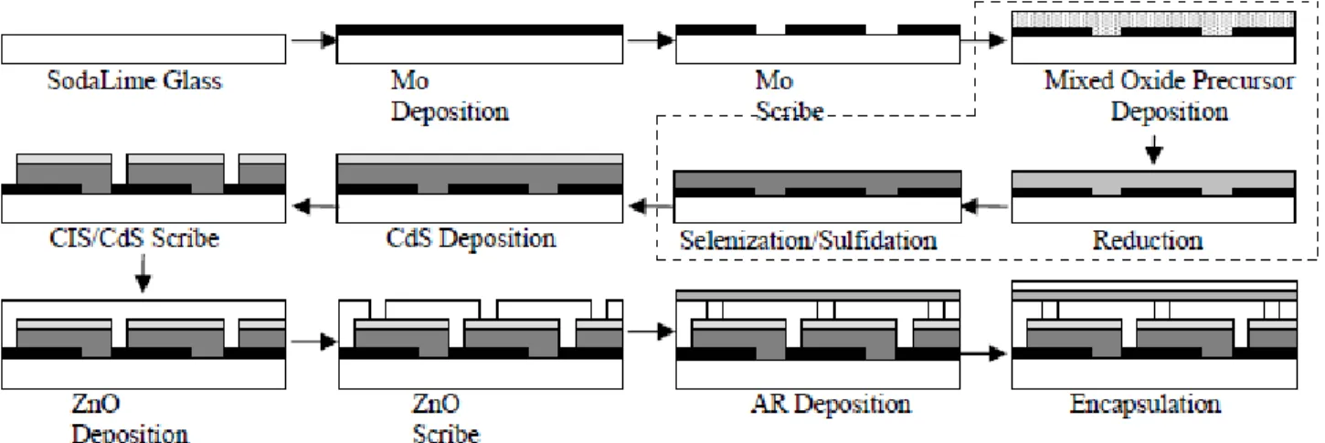
Figure 2. CIGS module fabrication process scheme.
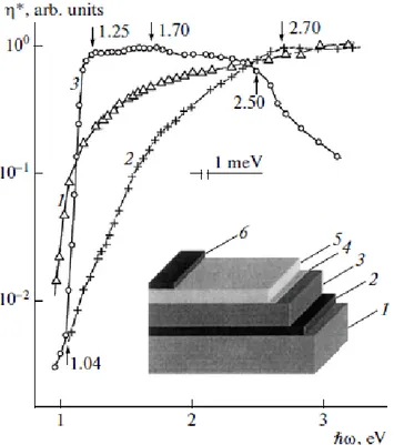
Figure 3. Spectral dependences of relative quantum efficiency for photoconversion η*(ħω) in thin_film solar cells ZnO/CdS/CIGS/Mo/polyimide (curves 1, 2) and ZnO/CdS/CIGS/Mo/glass (curve 3) in the case of illumination of the ZnO side of these cells with nonpolarized radiation at T = 300 K. Curves 1–3 are normalized to the absolute maximum of each spectra. Arrows at curves 1–3 indicate the energy position of spectral features. The basic structure of fabricated thin films solar cells is shown in the inset: (1) is the polyimide substrate (25 μm), (2) is the lower contact (1 μm), (3 is the active region (1.5 μm), (4) is the buffer CdS layer (30 μm), (5) is the ZnO/ITO window (0.5 μm), and (6) is the contact grid.
The low strength and high weight of glass substrates (the latter property completely excluding their use in spacecraft) can be highlighted as the main disadvantages of these types of substrates. It was for the elimination of the above disadvantages, primarily, that studies were begun with the aim of developing technology for the formation of CIGS films on substrates composed of lighter elements and, in particular, metal and polyimide substrates, which opens up new possibilities for a large reduction in the weight and an increase in the reliability of thin films solar cells. It should be stressed that further progress in realizing the benefits of thin films solar cells based on CIGS not only implies the development of new technologies but also requires further studies of the photovoltaic phenomena in solar cells. This will serve as a basis for the deliberate orientation of existing technology towards achieving the maximal (at present) quantum efficiency of photoconversion η*(ħω) for solar cells. The very replacement of rigid glass substrates by flexible ones (made of Cr, Mo, polyimide, and so on) requires the solution of new problems that
Kalmar, Sweden, November 26-28, 2012
constantly arise in the course of this specific next generation adjustment of the basics of thin films solar cells technology.
This study belongs to the range of those devoted to investigating the spectral dependences of the relative quantum efficiency of photoconversion in thin film ZnO/CdS/CuInGaSe2/Mo structures
formed on polyimide and glass substrates [2]. (I) Thin polycrystalline CIGS films with the thick ness ~1.7 μm were grown on the surface of a Mo film with the thickness ~2.5 μm, deposited on a ~2.5 μm-thick polyimide substrate (see the inset in Fig. 1). Evaporation was performed at the substrate temperatures Ts ≤ 480°C by thermal coevaporation of Cu(In, Ga)Se2 components in a
vacuum; the ratio of the elements Cu, In, and Ga (with a purity no lower than 99.999 wt %) corresponded to that required for efficient photoconversion of solar radiation. Simultaneously, fluxes of Se and Na (Na is from a NaF source) were obtained by coevaporation [6]. The Na concentration in the CIGS films was typically no higher than 0.1 at %. Then, a CdS film with the thickness ~40 nm was deposited by the chemical method onto the CIGS film surface. The final stage in this technological process for thin films solar cells fabrication consisted of the deposition of n thin intrinsic zinc oxide film i-ZnO onto the CdS film’s external surface; a film of heavily doped zinc oxide n-ZnO:Al (50 nm) was then deposited onto the i-ZnO film. The ZnO films were typically deposited by the magnetron method; such a combined method ensured the formation of a broad-band window with the aim of guaranteeing low optical losses in the case of optical radiation incident on the thin films solar cell surface.
(II) The crystal structure and phase composition of the obtained films were studied by X_ray structure analysis using a D-5000 diffractometer with CuKα radiation (α = 1.5418 Е), in the variation range of the angle 2θ 10° to 100°, at the scanning step ~0.01°. It is worth noting that the crystal lattice parameters for the obtained CIGS films were estimated from diffractogrammes and agree fairly well with the values known for these solid solutions. The phase composition was analyzed using the database of the Joint Committee on Powder Diffraction Standard (JCPDS). The elemental composition of the Cu(In, Ga)Se2 films was determined by the X-ray spectral
microanalysis (XSM) method with energy dispersion using a JEOL 6400 scanning electron microscope with error no larger than 2 at %.
Measurements of the stationary current–voltage (I–V) characteristics for the obtained thin films solar cells provides grounds for assuming that such structures feature pronounced rectification. The forward direction in these characteristics is independent of the substrate type used and always corresponds to the negative polarity of external bias applied to the front contact (see the inset in Fig. 1) for comparable types of thin film structures. It was established that, when the upper contact side of both types of thin films solar cells is illuminated (see the inset in Fig. 3), systematic features of the photovoltaic effect are practically the same in these structures. This circumstance may be indicative of the higher quality of thin films solar cells formed on glass substrates. The quantum efficiency of photoconversion in the soilar cells under comparison, which differ only by substrate material, as well. These data indicate that the largest value of η*(ħω) for structures based on CIGS films are still only featured by thin films solar cells formed on glass substrates. The main result of measurements of the photovoltaic parameters for flexible thin films solar cells formed on a polyimide film is that a SC on such a substrate did not exhibit any irreversible variations in the values of η*(ħω), which clearly indicates that there is no macroscopic disruption of the contact films’ integrity in the interface region. It should also be noted that our study was the first in which the relative quantum efficiency spectra for photoconversion η*(ħω) were investigated; these spectra are in fact ratios between the short-circuit photocurrent and the number of photons incident on the photodetecting surface of a thin films solar cells on polyimide.
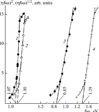
Figure 4. The dependences (η*(ħω))1/2 = f(ħω) (curves 1and 3) and (η*(ħω))2 = f(ħω) (curves 2 and 4) for thin films solar cells on glass (curves 1, 2) and on polyimide (curves 3, 4). T = 300 K.
In Fig. 3, we show the obtained (for the first time) spectral dependences of relative quantum efficiency in thin films solar cells based on Cu(In, Ga)Se2 films deposited on flexible (Fig. 1;
curves 1, 2) and rigid (Fig. 3, curve 3) substrates. We now distinguish the main systematic features, which follow from this comparison. So far, in studies devoted to investigating the effect of the CIGS solar cell transition from a rigid substrate to a flexible one on their photovoltaic properties, it was noted that such a procedure always induces a decrease in η*(ħω) but brings about an improvement in the weight factor of the photoconversion [3]. Consequently, it was established as a result of measurements of the first η*(ħω) spectra (Fig. 3) that the formation of thin films solar cells based on Cu(In,Ga)Se2 on flexible polyimide substrates (Fig. 3, curve 1)
brings about a decrease in the quantum efficiency of photoconversion. In order to assess the character and energy of inter band optical transitions in the two solar cell types under comparison, we also perform an analysis (generally accepted in such problems) of the edge photoactive absorption spectra’s form for the studied structures (Fig. 4) from the standpoint of the theory of fundamental absorption in diamond-like semiconductors [4,5]. Such an analysis provides grounds to assume that edge photoactive absorption in the Cu(In, Ga)Se2 is formed by
indirect and direct interband transitions in a case where the film grown on a rigid glass substrate exhibits, it seems, the highest quality. In the case of CIGS film growth on a polyimide substrate
Kalmar, Sweden, November 26-28, 2012
near its destruction temperature, the concentration of imperfections can greatly increase in the CIGS layer.
3 RESULTS AND DISCUSSIONS
We can assume that, in the case of a transition to CIGS film growth on polyimide, the ontribution of indirect transitions increases. As a consequence of this, the contribution of the direct interband transitions to the photoconversion process in thin films solar cells in the region of the maximum in the solar radiation spectrum decreases, therefore, the photoconversion efficiency starts to become lower than that characteristic of CIGS solar cells fabricated on glass substrates.
Thus, we studied (for the first time) the relative quantum efficiency of photoconversion for thin_film solar cells based on Cu(In, Ga)Se2 films grown on glass and polyimide substrates. The
specific features of photoactive absorption in two types of solar cells are discussed. It is established that a transition to flexible substrates causes a decrease in the relative quantum efficiency of photoconversion by thin_film solar cells based on CIGS solid solution films in the region of the maximum in the solar radiation spectrum.
The development of this research will be created completely new constructions of photovoltaic systems with expected conversion efficiency of 30-40% and an increase in electricity generation in the day by 20-60% due to the full utilization of the direct and scattered radiation and the corresponding 3D building photovoltaic systems. The results of research aimed at realization of a number experimental samples perspective types of thin-film solar cells and photovoltaic devices, which have opportunities to reduce the cost of products due to technological production, low cost and availability of raw materials, streamline manufacturing processes. As we can see, series-produced devices haven't got these opportunities.
Continuation of such project can form the basis of serial production of high performance solar inverters in power systems using spectral expansion, conversion and concentration of radiation, with the projected cost below the criterion at 1,00 USD $ per watt of installed capacity. This production will make it possible to use products in the climatic conditions of Russia and the Nordic countries (including Sweden).
This study was supported by the contract “Research and Development of Deposition System for CIGS Solar Cell” signed by the Ioffe Physical Technical Institute (Russian Academy of Sciences).
3 REFERENCES
[1] V. K. Kapur, B. M. Basol, C. R. Leidholm, G. Norsworthy, A. Halani and R. Roe, ‘Photovoltaics for the 21stCentury’ Proceedings Volume 99-11, 1999, pp 78 – 85, The Electrochemical Society, New Jersey, USA.
[2] V. Yu. Rud, Yu. V. Rud, and H._W. Schock, Solid State Phenom. 67–68, 421 (1999). [3] F. Kessler, D. Herrmann, and M. Powalla, Thin Solid Films 480–481, 491 (2005).
[4] S. Sze, Physics of Semiconductor Devices (Wiley Intersci., New York, 1981; Mir, Moscow, (1984).
[5] Yu. I. Ukhanov, Optical Properties of Semiconductors (Nauka, Moscow, 1977) (in Russian).