UPTEC E 20018
Examensarbete 30 hp
Juni 2020
SiC MOSFET function in DC-DC
converter
Teknisk- naturvetenskaplig fakultet UTH-enheten Besöksadress: Ångströmlaboratoriet Lägerhyddsvägen 1 Hus 4, Plan 0 Postadress: Box 536 751 21 Uppsala Telefon: 018 – 471 30 03 Telefax: 018 – 471 30 00 Hemsida: http://www.teknat.uu.se/student
Abstract
SiC MOSFET function in DC-DC converter
Christian Al KzairThis thesis evaluate the state of art ROHM SCT3080KR silicon carbide mosfet in a synchronous buck converter. The converter was using the ROHM P02SCT3040KR-EVK-001 evaluation board for driving the mosfets in a half bridge configuration. Evaluation of efficiency, waveforms,
temperature and a theoretical comparison between silicon mosfet (STW12N120K5) is done. For the efficiency test the converter operate at 200V input voltage and 100V output voltage at output currents of 7 to 12A, this operation was tested at switching frequencies of 50 kHz, 80 kHz and 100 kHz. The result of the efficiency test showed an efficiency of 98-97 % for 50 kHz, 97.7–96.4 % for 80 kHz and 97–96.2 % for the 100 kHz test. The temperature test shows a small difference in comparison of the best case scenario and the worst case scenario, temperature ranges from 25.5 to 33.5 °C for the high side mosfet while the low side mosfet temperature ranges from 29.8 to 35 °C. The waveform test was conducted at 50 kHz and 100 kHz for output currents of 4A and 12A (at 200V input and 100V output). The result of the waveform test shows a rise and fall time of the voltage in range of 10-12 ns while the current rise and fall time was 16ns for the 4A test and 20ns for the 12A test. Overall SiC mosfet shows a clear advantage over silicon mosfet both in terms of efficiency and high power capabilities.
ISSN: 1654-7616, UPTEC E 20018 Examinator: Mikael Bergkvist Ämnesgranskare: Johan Forslund Handledare: Konstantin Kostov
Sammanfattning
I detta examensarbete testades ROHM SCT3080KR kiselkarbid mosfets i en synkron bock omvandlare. Drivarkretsen ROHM P02SCT3040KR-EVK-001 användes för driva mosfetarna i en halvbrygga konfiguration. Verkningsgrad, vågformer och temperatur testades i ett praktiskt test och jämfördes med simuleringar, samt en teoretisk jämförelse mot en kisel mosfet.
Verkningsgraden testas med en inspänning på 200V och en utspänning på 100V, med
utströmmar mellan 7 till 12A, detta test genomfördes med en frekvens på 50 kHz, 80 kHz och 100 kHz. Verkningsgraden utgick till 98-97 % för 50 kHz, 97.7–96.4 % för 80 kHz och 97–96.2 % för 100 kHz. Temperaturökningen av den primära mosfeten utgick till 25.5–33.5 °C och den sekundära mosfetens temperatur utgick till 29.8–35 °C, dessa temperaturer är från lägst frekvens och lägsta ineffekt till högsta frekvens och högsta uteffekt. Mosfetarnas vågformer testades för utströmmar på 4A och 12A för frekvenserna 50 kHz och 100 kHz (med 200V ingång och 100V utgång). Stig resp. fall tid mättes till 10-12ns för spänningarna medan stig och fall tid för
strömmarna utgick till 16ns för 4A och 20ns för 12A. Överlag är kisel karbid mosfeten ett bättre alternativ för höga effekter och för applikationer som kräver hög verkningsgrad.
Acknowledgement
Firstly I want to thank Mats Wårdemark from Powerbox for making this master thesis possible, I have learned a lot with his help and consultation. I also want to thank Konsantin Kostov from Rise for helping me during this thesis, he has a very inspiring mentor and has always been available if I needed help. Because of Covid-19 I could not do any tests at Powerbox lab and for that I want to thank Johan Forslund from Uppsala universitet for making it possible to do tests at the university lab. Lastly I want to thank my friends and family for supporting me during this master thesis, they have been a great help and motivation.
Content
Nomenclature ... 1
1.0 Background and limitation ... 2
1.1 Thesis outline ... 3
2.0 Theory ... 4
2.1 Semiconductor ... 4
2.2 SiC vs Si ... 7
2.3 Mosfet ... 8
2.3.1 Mosfet conduction losses ... 9
2.3.2 Mosfet switching loss... 10
2.3.3 Mosfet gate losses ... 11
2.3.4 Mosfet total power loss ... 11
2.4 Previous studies... 12
2.5 Buck converter ... 13
2.6 Parasitic components of capacitor, inductor and mosfet package ... 18
2.6.1 Capacitor ... 18
2.6.2 Inductor ... 18
2.6.3 Mosfet package and PCB ... 19
2.7 Synchronous buck converter ... 20
2.8 Theoretical comparison between Si and SiC mosfet ... 21
3.0 Experimental/Simulation procedure ... 23
3.1 Setup for running buck configuration ... 24
3.2 Test procedure ... 26
3.3 Simulation test... 27
4.0 Measurement and simulation results ... 29
4.1 Efficiency result ... 29
4.1.1 200Vin 100Vo 50 kHz ... 29
4.1.2 200Vin 100Vo 80 kHz ... 30
4.1.3 200Vin 100Vo 100 kHz ... 30
4.1.4 Plecs conduction and switching losses... 31
4.2 Temperature result ... 31
4.3 Waveforms ... 32
4.3.1 200Vin 100Vo 50 kHz 4A output current ... 32
4.3.2 200Vin 100Vo 50 kHz 12A output current ... 33
4.3.3 200Vin 100Vo 100 kHz 4 A output current ... 34
4.3.5 Spice waveforms rise and fall time ... 36
4.3.6 Experimental waveforms rise and fall time ... 37
5.0 Discussion ... 38 5.1 Efficiency ... 38 5.2 Temperature ... 38 5.3 Waveforms ... 38 5.5 Future research ... 39 5.6 Conclusion ... 39
1
Nomenclature
Wide band gap/WBG – semiconductors that has higher band gap than 1-1.5 eV. DC – Direct current, current that does not alternate.
PE – Power electronics, the application of semiconductors to control or convert power. Mosfet – Metal Oxide Semiconductor Field Effect Transistor, an electronic switch. SiC – Silicon Carbide.
Si – Silicon.
Carriers – Electrons and holes in a semiconductor. FET – Field Effect Transistor.
HS – High side, (in reference to primary switch in a half bridge configuration) LS – Low side, (in reference to secondary switch in a half bridge configuration) PCB – Printed Circuit Board.
DMM – Digital Multimeter. PWM – Pulse width modulation. CLK – Clock signal.
2
1.0 Background and limitation
In a world that keeps demanding more energy efficient components, WBG materials has increased in demand with each year. The silicon carbide market is expected to grow from 749 million $ (2020) to 1812 million $ (2025).1 Today the biggest demand of WBG materials is from the EV market, this is because the EV market demands high power and efficient components.2 Fig 1:1 shows the expected SiC growth.
Fig 1:1 MarketsAndMarkets future projection of the demand of SiC3
This report evaluate silicon carbide mosfets. This project collaborates with Rise (Research institutes of Sweden) and Powerbox. The project was funded by Powerbox and Rise provided office space and a supervisor. The aim of the project was to see how efficient SiC mosfet are. To evaluate the system, a high power synchronous buck converter was used.
The manufacturer ROHM has developed an evaluation board for their SiC Mosfet. Evaluation board – P02SCT3040KR-EVK-001 (Half bridge evaluation board).
This evaluation board is compatible with the SCT3080KR mosfets and can be configured to use different topologies. The board has short-circuit protection, dead time injection and a snubber network, the board has the mosfets in a half bridge configuration.
1 Silicon Carbide Market by Device (SiC Discrete Device and Bare Die), Wafer Size (4 Inch, 6 Inch and Above, and 2 Inch), Application (Power Supplies and Inverters and Industrial Motor Drives), Vertical, and Region - Global Forecast to 2025
2 Ibid. 3 Ibid
3 The ROHM SiC Mosfet – SCT3080KR
The SCT3080KR is a state of the art SiC mosfet. This mosfet is mostly aimed towards the higher power usage such as power supplies, motor drives etc.
Parameters SCT3080KR
Table 1:1 SCT3080KR parameters
Drain-Source Voltage [V] 1200 Drain-source on-resistance @ 25 °C [mΩ] 80
Drain current [A] 31
Total power dissipation [W] 165
Turn on delay [ns] 5
Rise time [ns] 13
Turn off delay [ns] 20
Fall time [ns] 12
Thermal resistance [°C/W] 0.7
Time is a limiting factor and thus the focus points will be presented below
Focus points
Efficiency (with output power ranging from about 700-1200 W) Mosfet temperature
Mosfet drain-source voltages and current waveforms (at frequencies of 50 kHz and 100 kHz with output currents of 4A and 12 A).
Testing was be conducted both by simulations using LTSpice (waveforms) and Plecs
(efficiency). A practical test was conducted with the SiC mosfets to compare with the simulation models.
1.1 Thesis outline
In chapter 2.0 the theory of semiconductors and their parameters are presented, the difference between silicon and silicon carbide, the mosfet fundamentals, and previous studies about SiC mosfets. The theory behind the buck converter, the difference between a regular buck converter and a synchronous converter, the parasitical elements of capacitor, inductor and mosfet package. Lastly a theoretical comparisons between silicon mosfet and silicon carbide mosfet.
In chapter 3.0 the methodology of the test is presented and how the configuration setup of the ROHM evaluation board. Instruments that are used for the test, and lastly the simulation circuit layouts.
In chapter 4.0 the final presentation of the result consisting of the efficiency, temperature and the waveforms of the mosfets.
In chapter 5.0 the discussion and conclusion of the thesis, and proposed future work are presented.
4
2.0 Theory
2.1 Semiconductor
Before going into the mosfet, the fundamentals of semiconductor devices has to be understood. For the sake of simplicity this theory will use silicon.
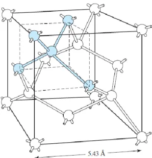
Silicon is structured as a crystal with a diamond structure. In the unit cell each silicon atom has four connections to other silicon atoms. Silicon has four valence electrons and share these electrons with its neighbors. This is why the silicon is sometimes called an “IV” material, because it belongs to the group of atoms that has four valence electrons.4 To form a crystal structure every unit cell is repeated in all directions. The unit cell has a cubic distance of 5.43 Å (seen in Fig 2:1).
Fig 2:1 Silicon unit cell.5
4Chenming Hu, Modern semiconductor devices for integrated circuits (Pearson,2009) p.2 5Chenming Hu, Modern semiconductor devices for integrated circuits (Pearson,2009) p.3
5
It is better to illustrate this model in 2D, looking at Fig 2:2 we can see the unit cell in 2D.
Fig 2:2 Silicon crystal in 2D, electrons represented as black dots.6
The structure shown in Fig 2:2 is under the assumption that the temperature is at 0K. This aspect is very important, if temperature is not at 0K then the thermal energy might lead to the silicon atom releasing one of its electrons, leaving a hole (positive charge) in its place.7 This free electron can conduct electricity. The minimum energy needed to release an electron is 1.1eV for silicon.
To increase the amount of free electrons/holes one can introduce doping.8 When doping is introduced it is possible to either dope with atoms that has more valence electrons than silicon or less. When silicon is doped with atoms that have five valence electrons, the four will bind to the silicon while the fifth electron can escape and be a free electron (conduct electricity). This kind of doping is called N type doping, for the silicon has more electrons than holes. Similarly doping with atoms that has three valence electrons is called P type doping.
To understand semiconductor more thoroughly it is needed to introduce the energy bands. Semiconductors has three energy bands, the valence band, band gap and conduction band. The valence band is the band that is full of charges while the conduction band has nearly none, between them are the band gap.
6 Ibid p.5 7Ibid p.5 8Ibid p.6
6
Fig 2:3 Energy band diagram of a semiconductor.9
The band gap is the minimum amount of energy needed to create an electron-hole pair. To calculate the band gap, subtract the conduction band energy level with the valence band energy level. The bands can be illustrated in Fig 2:3.
𝐸𝐺 = 𝐸𝐶− 𝐸𝑉 (1)
The band gap is the minimum amount of energy needed to create an electron-hole pair, and this energy can be from the environment such as thermal energy. This means that semiconductors that have high band gap can withstand higher temperatures.
When doping a semiconductor one can add more electrons or holes in the semiconductor. This is very important since it will determinate the conductivity of the semiconductor.
Eq.2 two is the conductivity of a semiconductor shows that it depends on the amount of free electrons and holes but also their respective mobility. The mobility (μ
)
is how mobile (freely moving) the carriers (holes/electrons) are. The q is the electric charge of an electron.𝜎 = 𝑞𝑛𝜇𝑛 + 𝑞𝑝𝜇𝑝 (2)
7
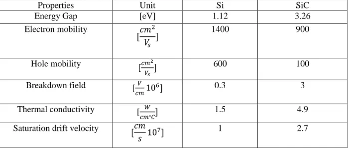
2.2 SiC vs Si
Silicon carbide offer some prominent benefits against silicon. This can be related down to the material differences.
Table 2:1 Semiconductor properties of Si and SiC10
Properties Unit Si SiC
Energy Gap [eV] 1.12 3.26
Electron mobility [𝑐𝑚 2 𝑉𝑠 ] 1400 900 Hole mobility [𝑐𝑚2 𝑉𝑠 ] 600 100 Breakdown field [𝑉 𝑐𝑚10 6] 0.3 3 Thermal conductivity [ 𝑊 𝑐𝑚°𝐶] 1.5 4.9
Saturation drift velocity [𝑐𝑚 𝑠 10
7] 1 2.7
Looking at Table 2:1 the following conclusions can be made for SiC. Higher band gap leads to higher temperature limit.
The breakdown field is ten times stronger, this allows SiC to have a high voltage limit. Since the breakdown field is stronger, the drift layer of the semiconductor can be made
thin, with a thin drift layer the on-resistance becomes very small while still maintaining a high breakdown limit (high drain-source voltage at low on-resistance).11
SiC has lower mobility on the carriers which require a higher gate voltage to obtain the lower on-resistance.12
The higher thermal conductivity allows for better cooling capabilities.
10 Rohm Semiconductor, “SiC Power devices and Modules application note”, 14103EBY01, (08-2014). P.3 11 Ibid.
8
2.3 Mosfet
Mosfet (metal oxide semiconductor field effect transistor), is a semiconductor device that is an electrical switch. The mosfet has a drain, source, gate, body and two intrinsic body diodes. The mosfet is a majority carrier device, this means that it only uses one type of charge carrier (either holes or electrons)13.
Fig 2:4 Mosfet N channel structure. Source, gate, drain, body and body diodes.14
The mosfet has intrinsic PN body diodes, one diode is connected with the body to the source and one diode from the body to the drain. The body diode that is connected from body to source get effectively shorted since the source and the body are wired together. Fig 2:4 illustrate the body diodes. Fig 2:5 shows the mosfet with its effective body diode and the circuit symbol.
Fig 2:5 N channel mosfet with body diode (left)15, circuit symbol of the n channel mosfet (right)16.
13 M.A. Laughton, D.F Warne. Electrical Engineer’s reference book, 16 ed. (Oxford: Newnes, 2002) cp 17 mosfet. 14 Alec Schmidt, edited by Robert Nelson, FET (Field-Effect Transistor), 28-12-2018.
15 Daniel W, Hart, Power electronics, (New York: The Mcgraw-hill Companies), p.9. 16 Wikimedia “Jjbeard”, IGFET symbol n enh, 01-06-2006.
9
The mosfet have some intrinsic parasitical components, these components can be divided between capacitive and resistive. The parasitical capacitance structure can be seen in Fig 2:6.
Fig 2:6 Parasitic capacitance of the mosfet (Cgd –gate to drain, Cgs – gate to source, Cds – drain to source).17
The drawback of the parasitical capacitance is that they can affect the switching of the device. The gate to source capacitance effects the gate losses, while the gate to drain and drain to source capacitance effects the switching of the device.18
The losses in the mosfet can be divided into three categories; conduction losses, switching losses and gate losses and the formulas presented below are valid for a half bridge buck converter.
2.3.1 Mosfet conduction losses
The conduction losses can be illustrated by having parasitical resistors in the drain (𝑅𝑑) and
source (𝑅𝑠).
Fig 2:7 Drain source parasitic resistance in mosfet19
These resistors (shown in Fig 2:7) results in heat loss by the current that goes through them. The power loss is equal to eq.3.
17 ROHM semiconductor, What are MOSFETs? – MOSFET Parasitic capacitance and its temperature
characteristic. 09-03-2007.
18 Ibid. 19 Hu. P.255
10
𝑃𝐶𝑜𝑛𝑑 = 𝐼𝐷2𝑅𝐷𝑆𝑜𝑛 (3)
Where
𝐼𝐷 is the drain current.
𝑅𝑑𝑠𝑜𝑛 is the drain-source parasitic resistance (𝑅𝑑 + 𝑅𝑠).
2.3.2 Mosfet switching loss
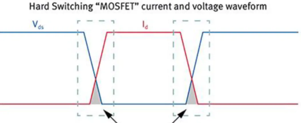
The switching losses in the mosfet is the grayed area in Fig 2:8.
Fig 2:8 Illustration of switching instance from off, then to on state and then back to off.20
As seen in Fig 2:8 the area where the drain current and drain voltage intersect is the total amount of energy lost during the switching instance. This is why a fast transition mosfet is important, the faster the mosfet can transition from its current state the smaller the loss area becomes.
𝑃𝑆𝑤𝑖𝑡𝑐ℎ =1
2∗ 𝑉𝐼𝑛∗ 𝐼𝑂∗ (𝑡𝑟+ 𝑡𝑓) (𝑃𝑒𝑟 𝑠𝑤𝑖𝑡𝑐ℎ𝑖𝑛𝑔 𝑖𝑛𝑠𝑡𝑎𝑛𝑐𝑒)
(4)
Where
𝑉𝐼𝑛 is the input voltage. 𝐼𝑂 is the output current.
𝑡𝑟 is the rise time.
𝑡𝑓 is the fall time.
11
2.3.3 Mosfet gate losses
Lastly the losses in the gate is the parasitic gate to source capacitance. This capacitance will introduce power loss presented in eq.5.
𝑃𝐺𝑎𝑡𝑒 = 𝑄𝐺 ∗ 𝑉𝐺𝑆 (5)
Where
𝑄𝐺 is the gate electric charge.
𝑉𝐺𝑆 is the applied gate source voltage
2.3.4 Mosfet total power loss
The total power loss in the mosfet for one switching cycle is equal to eq.6
𝑃𝑇𝑜𝑡 = 𝑃𝑐𝑜𝑛𝑑 + 𝑃𝑆𝑤𝑖𝑡𝑐ℎ+ 𝑃𝐺𝑎𝑡𝑒 (6)
To account for switching frequency and duty cycle the total power loss in the mosfet is equal to eq.7.
𝑃𝑀𝑜𝑠𝑡𝑜𝑡 = 𝑃𝑐𝑜𝑛𝑑𝐷 + (𝑃𝑆𝑤𝑖𝑡𝑐ℎ+ 𝑃𝐺𝑎𝑡𝑒) 𝑓𝑠𝑤 (7) Where
𝑓𝑠𝑤 is the switching frequency. 𝐷 is the duty ratio between 𝑉𝑜
12
2.4 Previous studies
To get and more thoroughly understanding of the efficiency of SiC mosfet, presented below are articles that has studied SiC mosfets in different toplogies.
An article from nov 2017 studied the different semiconductors in a boost configuration at output power of 50 W to 500 W with voltages ranging from 30, 50 and 72 V, with switching
frequencies of 20 kHz and 50 kHz.21 The efficiency from the article is documented in the Table 2:2
Table 2:2 SiC mosfet efficiency in boost converter
Input voltage (V) Efficiency (%) @ 20kHz Efficiency (%) @ 50kHz
30 89-95 86-93
50 90-96 87-94
72 90-97 88-96
A study in 2012 investigated a 1kW PV (Photovoltic) inverter where they used SiC mosfets and recorded an overall efficiency of 95.5 %.22 They also noted that the switching waveforms rise and fall time is in the nano scale.23
A test made by Cree (Wolfspeed) shows how effective SiC is at high temperature, since its on-resistance does not increase as much as compared to Si, the conduction losses will be much lower at higher temperature.24 This in itself will lead to higher efficiency at higher temperature
when compared to the Si mosfet. The report shows that the SiC mosfet on-resistance increased with 30% from 25 °C to 150 °C, while the Si on-resistance increased with 130 % from 25 °C to 150 °C.
21 Mohd Alam. Kuldeep Kumar. Viresh Dutta, Comparative efficiency analysis for silicon, silicon carbide
MOSFETs and IGBT devices for DC-DC boost converter, Springer Nature Switzerland AG 2019, 27-11-2019.
P.8-9.
22 Omid Mostaghimi. Nick Wright. Alton Horsfall, Design and Performance evaluation of SiC based DC-DC
converter for PV application, IEEE, 12-11-2012. P.4-6.
23 Ibid.
24 Yuequan Hu. Jianwen Shao. Teik Siang Ong, High-Frequency High-Power-Density Power converters with SiC
13
2.5 Buck converter
The conventional buck converter has an input voltage that is higher than the output voltage. In Fig 2:9 the conventional circuit layout is shown of a buck converter.
Fig 2:9 Buck converter circuit25
In every buck converter there is always an inductor, capacitor, load and semiconductor devices such as mosfet and diode.26 In the buck converter there are two stages where one can analyze the voltage and current waveforms. These stages are when the switch is on (closed and conducting) and off (open and no conduction). During the on time the capacitor and inductor charges up and on the off time they discharge their stored energy.
Power electronics circuits has two modes of operation, these are called CCM (continuous conduction mode) and DCM (discontinuous conduction mode). During CCM the output voltage and input voltage behave linearly. Then there is DCM which makes the output and input voltages behave nonlinear.
To guarantee that the circuit is always in the CCM the instantaneous inductor current should not reach below 0 A.
The analysis of the buck converter has to have these assumptions The circuit operates in steady state.
The inductor current is continuous (CCM).
The capacitor is assumed to hold a constant output voltage.
The electronic switch in the circuit is on for 𝐷𝑇 and off during (1 − 𝐷)𝑇. The components are ideal (no losses in the circuit).
25Hart, p.199 26Hart, p.198
14
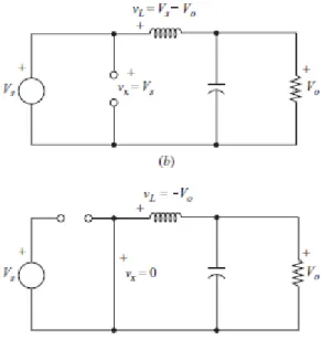
The circuit begins when the electric switch is closed. This means that the electric switch is represented as a short, and the diode is represented as open. When the circuit is in the off state, the switch is open and the diode is conducting. The on and off state can be illustrated in Fig 2:10.
Fig 2:10 Buck converter on state and off state27
The electric switch is closed for a duty duration of the total time
𝑡𝑜𝑛 = 𝐷𝑇 (8)
The inductor is charging linearly as according to eq.9
𝑉𝑠− 𝑉𝑜= 𝐿𝑑𝑖 𝑑𝑡
(9)
Arranging the total change of current in the inductor during the on state with eq 8 and eq.9.
𝛥𝑖𝐿𝑜𝑛 = (𝑉𝑠− 𝑉𝑜)𝐷𝑇 𝐿
(10)
The switch is then open for the rest of the time which is equal to eq.11.
𝑡𝑜𝑓𝑓 = (1 − 𝐷)𝑇 (11)
15 The voltage across the inductor is then equal to eq.12.
−𝑉𝑜= 𝐿𝑑𝑖 𝑑𝑡
(12)
Arranging the eq.11 and eq.12 to get the total change in the inductor during the off state.
𝛥𝑖𝐿𝑜𝑓𝑓 =−𝑉𝑜(1 − 𝐷)𝑇 𝐿
(13)
For steady state the total change in the inductor current has to be equal to zero. (𝑉𝑠− 𝑉𝑜)𝐷𝑇
𝐿 −
𝑉𝑜(1 − 𝐷)𝑇
𝐿 = 0
(14)
With eq.14 the output voltage can be solved to
𝑉𝑜= 𝑉𝑠𝐷 (15)
For steady state operation the average capacitor current is equal to zero. This means that the average inductor current is equal to the output current.
The average inductor current is equal to
𝐼𝐿 = 𝐼𝑅 =𝑉𝑜 𝑅
(16)
To get the inductor current max and min values eq.10 or eq.13 with eq.16 and that 𝑇 = 1/𝑓 can be used to get the inductor current variations.
𝐼𝐿𝑚𝑎𝑥/𝑚𝑖𝑛 = 𝐼𝐿±𝛥𝑖 2 (17) 𝐼𝐿𝑚𝑎𝑥/𝑚𝑖𝑛 = 𝑉𝑜(1 𝑅± 1 − 𝐷 2𝐿𝑓 ) (18)
To establish the inductor value the inductor current ripple can be used to determine the inductor value (eq.19) such that the operation is still in CCM.
𝐿 = 𝑉𝑜(1 − 𝐷) 𝛥𝑖𝑓
16
Fig 2:11 Voltage and current of inductor and capacitor current.28
When the switch turns off, the voltage across the inductor is equal to (𝑉𝑠− 𝑉𝑜) the inductor and
capacitor is charging up during this moment. When the switch turns off, the voltage across the inductor is −𝑉𝑜 the capacitor and inductor is then discharging their stored energies The output capacitor is used to minimize the ripple in the output voltage. The capacitor cannot hold the output voltage at a fixed voltage, it can only contain a fixed amount of charges which limits the total ripple in the voltage.
To get the total ripple relative to the output voltage, the total net charge in the capacitor can be used
𝛥𝑄 = 𝐶𝛥𝑉𝑜 (20)
The change of charge in the capacitor can be more easily explained by geometry. Since the change of current in the inductor/capacitor is an triangle (seen in Fig 2:11) the net charge depends on eq.21
𝛥𝑄 =1 2𝑏ℎ
(21)
Where
𝑏 is equal to the base of the triangle ℎ is equal to the height of the triangle
17
The base is equal to half of the total time and the height is equal to half of the inductor current variation, this leads to the total net change of charges in the capacitor equal to eq.22.
𝛥𝑄 =1 2 𝑇 2 𝛥𝑖 2 = 𝑇𝛥𝑖 8 (22)
Thus using eq.20, eq.22 and eq.10 or eq.13 the total ripple relative to the output voltage is equal to 𝛥𝑉𝑜 𝑉𝑜 = 1 − 𝐷 8𝐿𝐶𝑓2 (23)
For efficiency calculation the input and output powers are needed.
For the input power, the input voltage and input current is multiplied together.
𝑃𝑖𝑛 = 𝑉𝑖𝑛𝐼𝑖𝑛 (24)
For the output power, the output voltage and input current is multiplied together.
𝑃𝑜= 𝑉𝑜𝐼𝑜 (25)
Thus for efficiency eq.24 and eq.25 is used to get the buck efficiency to
η = 𝑃𝑜
𝑃𝑖𝑛
= 𝑉𝑜𝐼𝑜 𝑉𝑖𝑛𝐼𝑖𝑛
18
2.6 Parasitic components of capacitor, inductor and mosfet package
The capacitor and inductor discussed previously are assumed to be ideal, this means that the component contains only inductance or capacitance. Of course in the practical world this is not true, components have parasitical resistances and inductances that are unwanted and impacts the systems efficiency.
2.6.1 Capacitor
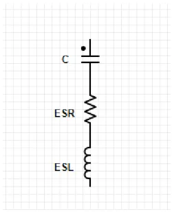
The capacitor includes both inductance and resistance, these are called ESL (equivalent series inductance) and ESR (equivalent series resistance). These parasitic element are frequency and temperature dependent.
Fig 2:12 Non ideal representation of an capacitor
In the ideal case the average capacitor current is equal to zero (in the buck converter scenario), but since there are ESR and ESL in the capacitor they will draw a certain amount of current. This current will affect the total efficiency since in the ideal case this current would instead go to the load of the system. With higher frequency and temperature, the parasitic can make an impact on the system efficiency. In most conventional capacitors that have datasheets, the manufacturer does state the resistance and inductance of the component at a certain frequency and temperature. To minimize the impact of the parasitic, choose capacitors such as film capacitors, the limitation with film capacitor is that they have a very limited capacitance. There are electrolytic capacitors that have higher capacitance but at the cost of higher ESR and ESL.
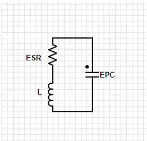
2.6.2 Inductor
The inductor does also have parasitic in form of ESR and EPC (Equivalent parallel capacitance). In most cases the ESR is the most dominant parasitic element. The ESR of the inductor will induce a voltage drop, this will lead to lower output voltage that effect the system efficiency. The EPC of the inductor becomes impactful at very high frequencies, this will make the inductor
self-19
resonate with the capacitance but this is in the MHz range, thus for lower frequencies the EPC can be neglected. The ESR of the inductor is hard to neglect since an inductor needs conductor wires, these wires can be chosen such that they have a very small resistance.
Fig 2:13 Non ideal representation of an inductor
2.6.3 Mosfet package and PCB
As previously discussed the mosfet has inherently parasitical capacitances. But in a practical scenario a mosfet is packaged and is soldered into a circuit board that has polygons and traces. These aspects introduces parasitical inductances, the inductance can influence the rise and fall time of the mosfet drain current.29 This effect also depends on the magnitude of the current that goes through the mosfet.30 Not only does it affect the rise and fall time, the parasitical inductance
can resonate with the parasitical capacitance of the mosfet which in turn induces ringing in the voltage waveforms, this ringing introduces high voltage spikes that can destroy the mosfet if the spike rises higher than the mosfets drain to source voltage limit.31
29 Alan Elbanhawy, Effect of source inductance on MOSFET rise and fall times, 25-03-2008, P.11 30 Ibid
20
2.7 Synchronous buck converter
In a synchronous configuration the diode is replaced with a mosfet. This is mostly done in high power system, specifically in low voltage/high current systems. The diode has a forward voltage drop that impacts on the total efficiency of the system. The difference between a mosfet and a diode is that a mosfet has a small drain to source resistance that will not drop the voltage as much in comparison to the diode forward voltage drop.
Fig 2:14 Synchronous buck converter.32
When S1 is conducting S2 is off. When the 𝐷𝑇 duration has passed S2 is conducting and S1 is off, S2 will be conducting for (1 − 𝐷)𝑇.
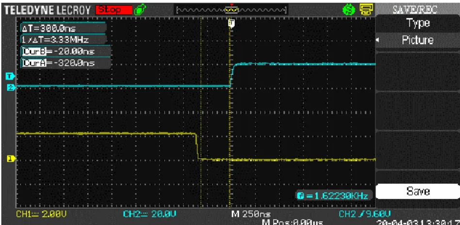
Synchronous switching also introduces difficulties in the driver circuit, since a diode is a passive component no external control is needed but with a mosfet there will be a need for a control signal to control the mosfet. There also has to be some dead time adjustment, dead time is needed to stop shoot through. Shoot through is a phenomenon when both the switches are on at the same time, this will lead to short between the source input and ground, the current will ramp up to a very dangerous level and might destroy the switches. Dead time will prevent shoot through by inputting a time between the switching instances, After one of the switches turns on/off then the dead time starts and both of the switches are off, when the dead time has passed the switch will turn off/on.
Fig 2:15 Dead time injection of the P02SCT3040KR-EVK-001 driver circuit, measured with a LeCory oscilloscope.
It’s also important to try and keep a low dead time. During the dead time period, current will flow from the output inductor through the second switch body diode. It is always good to adjust
21
the dead time such that it is the smallest amount of time needed to avoid shoot through but keep the losses to a minimum.
Another feature of the synchronous buck is that it can handle DCM without any issue. DCM in a conventional buck converter can lead to component damage, this is because the current in the inductor is negative. The inductor current cannot be discharged through the circuit diode, thus this will lead to an increasing voltage on the inductor (since the magnetic field stored in the inductor will collapse) that can come up to levels that might destroy the primary switching transistor or other components that can’t handle the high voltage level. Since the diode is replaced with a switch in a synchronous buck converter the negative current in the inductor can flow freely when the secondary switch turns on.
2.8 Theoretical comparison between Si and SiC mosfet
The silicon mosfet is the ST Microelectronics STW12N120K5. This mosfet is comparable to the SiC mosfet because of its matching drain to source voltage. Although they don’t have the same drain current capability this because of the fundamental limitation of silicon. The comparison was concluded on 200V input voltage, 100V output voltage and output current of 7-12A at respective 50 kHz and 100 kHz. Using eq.3 and eq.4 and accounting for switching frequency and duty cycle the losses are presented in Table 2:3. Price was from Mouser at time of Q2 2020.
Table 2:3 Theoretical comparison between Si and SiC mosfet
Parameters STW12N120K5 SCT3080KR
Drain to source voltage [V] 1200 1200 Drain current [A] @ 100 °C 7.6 22
Rds [mΩ] @ 25 °C 620 80
Rds [mΩ] @ 150 °C 1612 136
Input capacitance [pF] 1370 785
Output capacitance [pF] 110 75
Reverse transfer capacitance [pF] 0.6 35
Total gate charge [nC] 44 60
Gate source charge [nC] 7.3 11
Gate drain charge [nC] 30 31
Rise time [ns] 11 13 Fall time [ns] 18.5 12 Conduction loss [W] @ 25 °C 15.19-44.64 1.96-5.76 Conduction loss [W] @ 150 °C 39.49-116 3.33-9.79 Switching loss @ 50kHz [W] 1.03-1.77 0.86-1.5 Switching loss @ 100kHz [W] 2.07-3.54 1.75-3 Price 1Qty [€] 6.85 18.27
From Table 2:3 the most important values that can be extracted are the drain current,
on-resistance, conduction losses and cost. The Si mosfet can conduct much less current than the SiC mosfet. The on-resistance of the Si mosfet is 7.8 times higher than the SiC mosfet at 25 °C, and at 150 °C the Si mosfet on-resistance increases with 160 % while the SiC mosfet on-resistance increases with 70 %. This is the reason why the conduction losses are much higher in the Si mosfet, the SiC mosfet will sustain a higher efficiency at higher temperature. Regarding the costs
22
the SiC mosfet cost almost three times the price of the Si mosfet, although the price is high this can be justified with having a smaller system volume (heatsink, capacitor and inductor) but also the fact that if a system where to use Si mosfet for very high current application then the need for multiple parallel mosfets were needed which in turn increases driver difficulty and volume. This comparison shows that SiC is a much better value when used in applications that has volume constraints. Although for lower current applications the Si mosfet can be cost-efficient if there is enough cooling capacity and if the system allows for a less efficient system.
23
3.0 Experimental/Simulation procedure
The setup consist of the evaluation board P02SCT3040KR-EVK-001, the output consist of a custom designed PCB that integrates the inductor, capacitor and the load to keep the total volume small and to minimize the usage of cables.
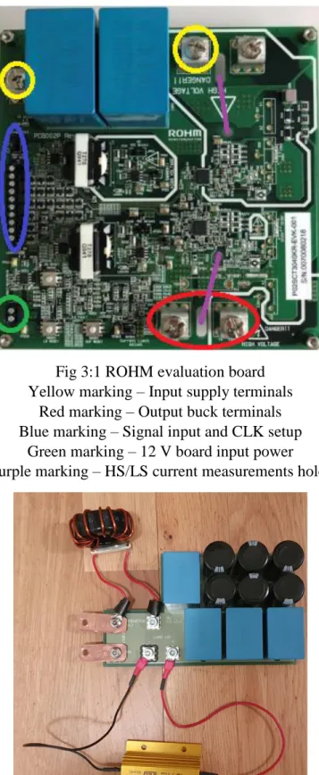
Fig 3:1 ROHM evaluation board Yellow marking – Input supply terminals
Red marking – Output buck terminals Blue marking – Signal input and CLK setup
Green marking – 12 V board input power Purple marking – HS/LS current measurements holes
24
3.1 Setup for running buck configuration
The ROHM evaluation board can be set up for numerous topologies, the synchronous buck configuration was used for this project.
The board has 3 pins located in the top blue marking in Fig 3:1, these pins are shown in Fig 3:3. The pins controls the terminals (CN201 shown in Fig 3:4) of the input clock signal, the
evaluation board can control the mosfets individually by using two separated signals (Dual-CLK mode) or by controlling them by using a single signal (Single-CLK mode). For a buck
configuration only one signal is needed thus the JP201 has to be set to “Single-CLK” this is done by using the jumper and connecting the middle pin and the “Single-CLK” pin together.
Fig 3:3 JP201 pins corresponding to which input the CLK signal will go on CN201 terminals.
The next step was to set up the CN201 10 pin screw terminal (Fig 3:4), only 4 pins are used for this configuration. Pin 01, 02, 03 and 05 or 10. To enable the board the enable pin (pin 01) must be set to ground, this can be made with a cable connected to pin 02 which is ground. The signal generators PWM power cable will go to pin 03 and the corresponding ground pin of the PWM signal can either be put to pin 05 or 10.
25
Fig 3:4 CN201 CLK input terminal.
There is also a power scheme of the evaluation board. To power up the system the driver was powered first then the presented clock signal cables are inserted to CN201 and then lastly the input power supply is connected.
When powering down the system the input power supply is turned off, then the clock signal generator is turned off and lastly the driver board power connections are unconnected.
The following equipment are used for testing.
Table 3:1 Instrument for measuring
Input voltage Fluke 175
Input current Tenma 72-2590
Output voltage Fluke 115
Output current 1m ohm shunt resistor measured by Tenma 72-9280
Thermometer Fluke 561 (IR)
Signal generator GwInstek SFG-1013
DC auxiliary supply GwInstek GPS-3303
Oscilloscope GwInstek GDS-2064
Input power supply Terco MV1300
Output load Terco MV1100
Mosfet drain to source voltage probes 2x Pico TA041 (1/100)
26
3.2 Test procedure
The component/parameters used for the experiment/tests can be seen in Table 3:2
Table 3:2 Test parameters and components
Inductor 3 inductor connected in series, total of 41uH (ESR 0.2 ohm)
Capacitor Custom made PCB, total of 1740uF (ESR 1.35 mohm, ESL 7.5 nH)
Load (Efficiency test) The load will be adjusted such that the average output current is from 7 to 12A Load (Waveform test) The load will be adjusted such that the
average output current is 4 and 12A Frequency (Efficiency test) 50 kHz, 80 kHz, 100 KHz
Frequency (Waveform test) 50, 100 kHz
Input voltage 200 ± 1V
Output voltage 100 V (50 % duty cycle)
The testing procedure begins with 10V as input voltage and then slowly ramping up the voltage to 200V. After the 200V has been set, adjusting the load to get the 7A output current. When the output current has been established the temperature testing is set by having a 2 minute timer, after the 2 minutes has gone the temperature of the high side and low side mosfet is measured. After taking the temperature measurements, adjust the load such that the output current is at 8A. Repeat the same procedure with the same 2 minute timer until all data has been gathered up to 12A (with 1A step) for all frequencies.
When the current and voltages has been documented eq.24, eq.25 and eq.26 is used to calculate efficiency.
The waveforms that will be documented is for output currents of 4A and 12A, for frequencies of 50 kHz and 100 kHz. The measurement equipment consist of the two Pico differential probes that measure the voltages of the switches, the Rogowski probe measure either the LS current or the HS current.
27
Fig 3:5: Experimental setup
Left side: The output PCB with a shunt resistor and a DMM measuring output voltage. Middle side: Is the evaluation board with mosfets, heatsink, fan and probes.
Right side: Input power supply cables with DMM measuring input voltage.
3.3 Simulation test
For the simulations the Spice and Plecs models from Rohm were used. These are located at their tool page of the SCT3080KR (
https://www.rohm.com/products/sic-power-devices/sic-mosfet/sct3080kr-product/tools).
These models were acquired during 03-2020, thus do not account for future changes made by Rohm of that date.
28
Fig 3:6 Spice simulation circuit
Fig 3:7 Plecs simulation circuit
Fig 3:6 shows how the LTspice simulation circuit, the load is a current sink which ramps the amount of drawn current such that it simulates the real test. The circuit simulates for 17ms but starts to record the data after 15ms.
Fig 3:7 show the Plecs simulation, the difference between the Plecs and LTspice is the blue area which represent a heatsink, this is so that thermal losses can be calculated.
Both of these circuits takes account for the driver dead time (300ns) and driver resistance (3.3Ω), the ESR and ESL for the capacitors and the ESR for the inductors.
29
4.0 Measurement and simulation results
The experimental tests consists of 3 kinds of experiments, efficiency test compared with Plecs simulation, temperature test (using Fluke 561) and waveform comparison with LTspice. For all tests the input voltage was 200V and 100V output voltage, the changing variables are current and switching frequency.
4.1 Efficiency result
The efficiency tests are made by measuring the input power by using eq.24 and the output power with eq.25 and then calculating the efficiency with eq.26, with this the efficiency plots are presented in Fig 4:1 to 4:3. The simulated efficiency is based on Plecs simulation that are using the same formulas as the experimental test. In Fig 4:4 the conduction and switching losses were plotted from the Plecs simulation.
4.1.1 200Vin 100Vo 50 kHz
30
4.1.2 200Vin 100Vo 80 kHz
Fig 4:2 Efficiency of simulation and experiment at 80 kHz
4.1.3 200Vin 100Vo 100 kHz
Fig 4:3 Efficiency of simulation and experiment at 100 kHz
Looking at Fig 4:1-4:3 we can see that the experimental efficiency lies between 98 %-96.2 %. The simulated efficiencies of 80 kHz and 100 kHz were matching the Plecs simulations (with a small discrepancy) while the 50 kHz Fig shows a larger discrepancy between the tested and simulated efficiencies. The efficiency in the experiments of 50 kHz and 80 kHz is higher than the simulated efficiency. The experiment was conducted twice to ensure no errors were made.
31
4.1.4 Plecs conduction and switching losses
Fig 4:4 Plecs simulations conduction and switching losses
Looking at Fig 4:4 we can see that the simulations shows increasing conduction losses (o-line) for higher output current which was expected. Increasing the switching frequency increases the switching losses (∇-line), this can be observed clearly when comparing the 100 kHz with 80 kHz and 50 kHz.
4.2 Temperature result
The experimental temperature test was measured by using the Fluke 561 IR thermometer. As presented in the methodology the temperature test was measured after 2 minutes for each increment of 1A.
32
Fig 4:5 and 4:6 shows how the temperatures of the high side mosfet and low side mosfet on different frequencies and output currents. The temperature increased for higher output current and higher switching frequencies which was expected. What is interesting is that the low side mosfet the temperature difference was smaller between the switching frequencies, this is
happening since the low side mosfet switches on small voltage (only body diode voltage) which means that the temperature increasing was primarily of the conduction losses.
4.3 Waveforms
The waveforms presented down below are the switching instances of the high side mosfet and low side mosfet. The high side mosfet (HS) indicates a turn off transition, while the low side mosfet (LS) indicates a turn on transition. The aim of these waveforms are to observe the difference between the simulation and experimental transition times and ringing effects. The transition times cannot be seen in the plots since the whole waveforms transition are present which makes the time scale larger than the transition scale. For this the transition times are calculated manually and presented in a Table 4:1 and 4:2.
4.3.1 200Vin 100Vo 50 kHz 4A output current
33
Fig 4:9 Test waveform turn off Fig 4:10 Test waveform turn on
4.3.2 200Vin 100Vo 50 kHz 12A output current
34
Fig 4:13 Test waveform turn off Fig 4:14 Test waveform turn on
4.3.3 200Vin 100Vo 100 kHz 4 A output current
35
Fig 4:17 Test waveform turn off Fig 4:18 Test waveform turn on
4.3.4 200Vin 100Vo 100 kHz 12 A output current
36
Fig 4:21 Test waveform turn off Fig 4:22 Test waveform turn on
What can be observed in Fig 4:7-4:22 are mostly how the waveforms are affected by the parasitical inductance of the package and evaluation board PCB, which resonate with the
parasitical capacitance and thus produce ringing effects on the voltages, this is mostly visible on the HS mosfet where a high voltage spike is present.
4.3.5 Spice waveforms rise and fall time
Table 4:1 Spice simulation waveforms rise and fall time
Test case Vds rise[ns] Vds fall [ns] Current fall [ns] Current rise [ns]
4A 50kHz 7.68 7.68 8.00 8.48
12A 50kHz 7.2 7.2 6.1 6.96
4A 100kHz 9.08 9.08 9.86 9.14
37
4.3.6 Experimental waveforms rise and fall time
Table 4:2 Experimental waveforms rise and fall time
Test case Vds rise[ns] Vds fall [ns] Current fall [ns] Current rise [ns]
4A 50kHz 10.4 10.8 16.4 16.8
12A 50kHz 10 10.8 19.6 20.4
4A 100kHz 12 12.4 16.1 15.2
12A 100kHz 11 11.2 20 20.8
The transition tables are calculated by measuring the time difference between 90% and 10% of the maximum waveform magnitude.
Looking at Table 4:1 and 4:2 we can observe a higher rise and fall time on all respective parameters when comparing the experimental and simulated values. For the currents we can observe that for higher currents the rise and fall time increases, this is because of the parasitical inductance that makes a larger influence when the current is higher.
38
5.0 Discussion
5.1 Efficiency
The efficiency of the experimental data shows us that our experiment were in the ranges that previous studies [11] [12] has shown. The experimental test were conducted twice to make sure no measurement error is present in the data. Interestingly Fig 4:1 and 4:2 shows that the
experimental efficiency was higher than the simulated efficiency. In the experimental test we note oscillations in the waveforms that would increase the switching losses, since the simulations do not have any parasitical inductance, oscillations cannot be induced thus the losses should be lower and the total efficiency should be higher in the simulation than the experimental
efficiency. This would make me incline that the reason for a lower simulated efficiency is because of deviation in the representation of the system in the simulation. At the same time the 100 kHz simulation is showing an accurate estimation of the experimental efficiency. If there was inconsistencies with the model of the simulations these would have been present in the 100 kHz simulations. This makes it harder to analyze where the error might be.
5.2 Temperature
The temperature test might have some small deviations because of the Fluke 561 IR laser getting reflected from the surface of the mosfets, to minimize the reflection of the laser, black electric tape was taped on the mosfets package. Although this solution does not mitigate the issue fully but can still give consistent data. It would have been interested to see how the Plecs simulate the temperature of the mosfets but alas since the thermal resistance of the heatsink and the capacity was unknown and the fact that a fan was used makes it hard to simulate the heatsinks properties. The experimental test could ignore the usage of the fan to increase the temperature but this would not affect the losses with a large magnitude. If we were to use the assumption that without the fan the temperature was around 100 °C the on-resistance would only increase to 100 mΩ and which in turn would have increase the conduction losses with 25 % since the on-resistance increases from 80 mΩ to 100 mΩ. This realizes in around 5 W more in conduction losses (in the 12A scenario) which would not impact the total efficiency that much when considering that Pin ≈ 1200 W.
5.3 Waveforms
As presented in the experimental waveforms the oscillations were present, but also the fact that the increase of rise and fall time were also present which the previous study [14] shows. The voltages transition times were lower than the specified datasheet values (𝑡𝑟 = 13𝑛𝑠, 𝑡𝑓 = 12𝑛𝑠) but since the timings are a bit lower they are still comparable to the datasheet values and I would incline to say that the values recorded are in line with what the datasheet specifies.
39
5.5 Future research
This thesis has focused on output currents of 7-12A at output voltages of 100 V. This is a relative low power of what the device is actually capable of. It would be more interesting to see how this device can handle higher output powers, both in regards to higher voltages and currents.
SiC is generally a much newer technology compared to silicon, so it would be in interesting to see how the SiC mosfet handle tests in longer durations.
This thesis has used Rohm mosfets and a Rohm driver, it would be interesting to see how the mosfets works with independently made drivers. That way one can test and see if the
performance of the mosfet is still consistent with a different driver.
5.6 Conclusion
This thesis has evaluated SiC mosfet in a synchronous buck converter at output currents of 7-12A with an input voltage of 200V and output voltage of 100V. The converter was also tested at different switching frequencies of 50 kHz, 80 kHz and 100 kHz. The result of the testing
concludes that the efficiency of the buck ranging between 98-96 %. This result matches previous studies of the SiC mosfets. It is also found that the waveform characteristics of SiC mosfets is in range of 10-20 ns.
In conclusion, this thesis shows that SiC has capabilities of being better than Si mosfets. For high power and high efficient systems the SiC mosfet higher cost can be justified by a smaller system volume, reduction in amount of needed mosfets and the capability of sustaining higher voltages and currents.
40
Bibliography
[1] MarketsAndMarkets, 02-2020
<
https://www.marketsandmarkets.com/Market-Reports/silicon-carbide-electronics-market-439.html> (Acc. 23-05-2020).
[2] Chenming Hu, Modern semiconductor devices for integrated circuits (Pearson, 2009). [3] ROHM semiconductor, SiC power devices and Modules, 09-2014
<http://rohmfs.rohm.com/en/products/databook/applinote/discrete/sic/common/sic_appli-e.pdf>
(Acc. 21-03-2020).
[4] M.A. Laughton, D.F. Warne, “Electrical engineer’s reference book’, 16 ed (2002), cp 17. [5] Alec Schmidt (Edited by Robert Nelson), FET (Field-Effect transistor), 28-12-2018
<https://www.digikey.com/eewiki/pages/viewpage.action?pageId=49414403>
(Acc. 18-06-2020).
[6] ROHM semiconductor, Body diode characteristics, (07-12-2017)
<https://techweb.rohm.com/knowledge/sic/s-sic/04-s-sic/6147> (Acc. 28-05-2020).
[7] Daniel W. Hart, Power electronics, (The McGraw-Hill companies, 2011).
[8] Wikimedia “Jjbeard”, IGFET symbol n enh, (01-06-2006).
< https://commons.wikimedia.org/wiki/File:IGFET_N-Ch_Enh_Labelled.svg> (Acc. 07-05-2020).
[9] ROHM semiconductor, What are MOSFETs? – MOSFET Parasitic capacitance and its
temperature characteristic. (09-03-2017).
<https://techweb.rohm.com/knowledge/si/s-si/03-s-si/4873> (Acc. 08-05-2020).
[10] Von Steven Keeping, A Review of Zero-voltage switching and its importance to Voltage
regulation, (05-08-2014)
<
https://www.digikey.be/de/articles/a-review-of-zero-voltage-switching-and-its-importance-to-voltage-regulation> (Acc. 19-04-2020).
[11] Mohd Alam. Kuldeep Kumar. Viresh Dutta, Comparative efficiency analysis for silicon,
silicon carbide MOSFETs and IGBT device for DC-DC boost converter, 27-11-2019.
[12] Omid Mostaghimi. Nick Wright. Alton Horsfall, Design and Performance evaluation of SiC
based DC-DC converter for PV application, IEEE, 12-11-2012.
[13] Yuequan Hu. Jianwen Shao. Teik Siang Ong, High-Frequency High-Power-Density Power
converters with SiC MOSFETs, Cree Wolfspeed (APEC industrial slides), 19-03-2020.
[14] Alan Elbanhawy, Effect of source inductance on MOSFET rise and fall times, 25-03-2008.