FPGA-Based
Hardware-In-the-Loop
Co-Simulator Platform for
SystemModeler
Master of Science Thesis in Electrical Engineering
FPGA-Based Hardware-In-the-Loop Co-Simulator Platform for SystemModeler Miguel Acevedo Sanz
LiTH-ISY-EX--16/5013--SE Supervisor: Mario Garrido
isy, Linköpings universitet
Leonardo Laguna
Wolfram MathCore
Examiner: Kent Palmkvist
isy, Linköpings universitet
Division of Computer Engineering Department of Electrical Engineering
Linköping University SE-581 83 Linköping, Sweden Copyright © 2016 Miguel Acevedo Sanz
This thesis proposes and implements a flexible platform to perform Hardware-In-the-Loop (HIL) co-simulation using a Field-Programmable-Gate-Array (FPGA). The HIL simulations are performed with SystemModeler working as a software simulator and the FPGA as the co-simulator platform for the digital hardware design. The work presented in this thesis consists of the creation of: A communi-cation library in the host computer, a system in the FPGA that allows implemen-tation of different digital designs with varying architectures, and an interface between the host computer and the FPGA to transmit the data. The efficiency of the proposed system is studied with the implementation of two common digital hardware designs, a PID controller and a filter. The results of the HIL simula-tions of those two hardware designs are used to verify the platform and measure the timing and area performance of the proposed HIL platform.
Furthermore, the possibility to use the proposed system as a co-processor of the software simulator in order to reduce the computation time of certain algorithms is also studied.
This thesis has been performed in collaboration with the company Wolfram Math-Core which is the developer of SystemModeler software simulator.
First I would like to thank Wolfram MathCore for the opportunity they gave me to do this master thesis with them and for the great work environment in their office in Linköping. From Wolfram I want to thank specially to my supervisor Leonardo Laguna and to Jan Brugård for their support during my thesis. I also want to give special thanks to my supervisor in ISY, Mario Garrido, for his help and inspiration.
And finally, I want to express my deepest gratitude to my family for all their support during my student years.
Linköping, September 2016 Miguel Acevedo
List of Figures ix
List of Tables x
Notation xi
1 Introduction 1
1.1 Motivation and purpose . . . 3
1.2 General requirements . . . 4
1.3 Problem statement . . . 5
1.4 Report overview . . . 5
2 Background and theory 7 2.1 Background of the HIL simulations . . . 7
2.2 On HIL simulations . . . 9 2.2.1 General concepts . . . 9 2.2.2 Synchronization . . . 11 3 System design 15 3.1 General design . . . 15 3.1.1 Host computer . . . 16 3.1.2 Interface . . . 17 3.1.3 FPGA HIL . . . 17
3.2 Specific requirements for the design components . . . 19
4 Design implementation 21 4.1 Host computer . . . 21 4.1.1 Modifications in SystemModeler . . . 22 4.1.2 ModelPlug . . . 25 4.2 Interface . . . 30 4.2.1 SPI . . . 30 4.3 FPGA system . . . 34 4.3.1 General parameters . . . 34 vii
viii Contents 4.3.2 Data handling . . . 35 4.3.3 Control . . . 37 4.3.4 Synchronization . . . 39 4.3.5 Serial-parallel converter . . . 40 4.3.6 DUT . . . 42
5 Results and discussion 45 5.1 PID . . . 45
5.1.1 PID theory . . . 45
5.1.2 SystemModeler implementation . . . 47
5.1.3 Results . . . 48
5.2 Filter . . . 57
5.2.1 Biquad filter theory . . . 57
5.2.2 SystemModeler implementation . . . 60 5.2.3 Results . . . 61 6 Conclusions 65 6.1 Conclusions . . . 65 6.2 Future work . . . 67 Bibliography 69
2.1 Summarized graph for the model-based-design methodology. . . . 9
2.2 Simplified diagram of the elements that constitute a HIL simulation. 10 2.3 Diagram of the main components of a electric motor. . . 11
2.4 Diagram for the time step synchronization mode. . . 12
2.5 Diagram for the master-slave synchronization mode. . . 13
3.1 Elements of the system . . . 16
3.2 FPGA system . . . 18
4.1 Interaction between the host computer elements . . . 22
4.2 Diagram representation of the three SystemModeler classes. . . 22
4.3 Configuration parameters for the FPGA class. . . 23
4.4 Configuration parameters for the input and output classes. . . 24
4.5 Communication layers of ModelPlug. . . 25
4.6 Composition of the transmission packets. . . 28
4.7 SPI communication protocol for mode 0. . . 30
4.8 Interface set-up . . . 31
4.9 Receiver FSM . . . 32
4.10 Transmitter FSM . . . 33
4.11 FPGA system . . . 34
4.12 Data handler block . . . 36
4.13 Control FSM . . . 37
4.14 Synchronization block FSM . . . 39
4.15 Serial-Parallel converter block . . . 41
5.1 Digital PID . . . 46
5.2 PID in SystemModeler . . . 47
5.3 PID in FPGA . . . 48
5.4 Virtual and FPGA PIDs comparison . . . 49
5.5 Variation of configuration parameters in the model . . . 49
5.6 Variation of configuration parameters in the FPGA . . . 50
5.7 Effect of the variation of the T . . . 51
5.8 Relation between the total computation time and the number of events. . . 53
5.9 Partial times communication . . . 54
5.10 Biquad direct form 1 . . . 58
5.11 Biquad direct form 2 . . . 58
5.12 SystemModeler implementation of the filter. . . 60
5.13 FPGA implementation of the filter. . . 61
5.14 Square input pulse . . . 62
5.15 Frequency response for the modelled filter . . . 62
5.16 Frequency response for the FPGA filter . . . 63
5.17 Time response for the modelled filter . . . 64
5.18 Time response for the FPGA filter . . . 64
List of Tables
4.1 Functions of ModelPlug . . . 295.1 Sampling time effects . . . 52
5.2 Sample size effects . . . 53
5.3 Sampling size effects for 16 bits data packets . . . 55
5.4 Area resources used in the Altera Cyclone II 2C20 FPGA. . . 56
5.5 Area resources used in the Xilinx Spartan 6 LX9 FPGA. . . 56
Abbreviations
Abbreviation Meaning
dut Design Under Test
dsp Digital Signal Processor ecu Electronic Control Unit fifo First-In First-Out
fsm Finite State Machine
fpga Field-Programmable Gate Array gpio General-Purpose Input/Output
hil Hardware-In-the-Loop (simulation)
hw Hardware
jtag Joint Test Action Group
mac Media Access Control (sub-layer) miso Master Input - Slave Output mosi Master Output - Slave Input
pci Peripheral Component Interconnect
pid Proportional, Integral, Differential (regulator)
ram Random-Access Memory
rx Receiver
sclk Serial Clock
spi Serial-Parallel Interface
ss Slave Select
sw Software
tx Transmitter
usb Universal Serial Bus
uut Unit Under Test
1
Introduction
Electronic devices form a big part of current technology nowadays. Since the invention of the transistor, the use of electronics is growing in an extraordinary manner. More specifically, digital electronics are becoming more and more pop-ular among designers because of its flexibility, reliability and easiness to design. However, one of the barriers for these systems is how to test and verify them. The testing phase for digital electronics and electronics in general is costly and time consuming. This costly and time consuming process is a problem in mod-ern day industry where increased competition between global companies create a need for short product development cycles. The most common solution is the simulation of electronic systems using virtual mathematical models. These sim-ulation models are widely used for validation and verification of electronic sys-tems during development phases. Nevertheless, simulations using virtual models produces two issues: First, it could be unfeasible for complex electronic designs, where it could be difficult to create a valid mathematical model for the electronic component developed. Second, the behavior of the virtual model could differ from the real implementation. This difference, even if is small, could cause a loss of accuracy during the verification process.
A method developed to solve these issues are the hardware-in-the-loop (HIL) simulations. These simulations consist of the addition of one more element to the simulation loop; a real hardware component. In other words, hardware-in-the-loop simulations are a co-simulation of two main elements: A physical hard-ware component and a mathematical model that represents the complete system which the hardware component is part of. The integration of a real component in a simulation model gives many advantages to the testing phase of a design. For example, this type of simulations increase the quality of the test by integrating the real hardware component. The results from a simulation are always more
2 1 Introduction
realistic when using the real physical component than a virtual model. Addition-ally, HIL simulations give a safe platform to perform tests and verification of a system. This is especially useful for controllers of critically safe systems where a malfunction can cause the loss of the complete system. HIL simulations are the best solution for these cases, the real controller can be tested in an reliable man-ner without the need of risking the complete physical system by using a virtual model of that complete system. Other benefits of using HIL simulations during the design and testing phases is the improvement of the project development times. When developing a complex system that is composed of several compo-nents, HIL simulations allow the development of those sections in a parallel way. This is because the different sections can be developed and tested with models of their counterparts without the need of having them already finished. Then, using HIL simulations, the iteration time and costs between different models is highly reduced. All these reasons make the HIL simulations a suitable validation test-bench for digital designs.
Nonetheless, even with the use of hardware-in-the-loop simulations during the development period, the time to create a electronic digital design is still long. When creating and testing digital designs, specially for Application-Specific-Inte-grated-Circuits (ASICs), the main bottleneck is the fabrication of the prototype. The fabrication of an ASIC is costly and time-consuming, and costs and time are increased if several iterations are needed during the developing period. A solution for these time and cost problems during development are Field-Pro-grammable-Gate-Arrays (FPGAs). A FPGA board is a configurable integrated circuit that can be reprogrammed with different digital designs. The FPGAs are formed by configurable logic elements that are connected with programmable interconnections. The rearrange of these elements and the interconnections al-lows the implementation of different digital designs in a fast and simple way. To perform this configuration of the FPGAs are usually used Hardware Description Languages (HDL) such as VHDL or Verilog. FPGAs allow to test and implement the different iterations during the design phase without modifying the hardware, which reduces time and cost problems of having to implement many prototypes during the developing period. The FPGAs are, therefore, an ideal platform for the implementation and test of digital designs and are commonly used for HIL simulations of digital electronics.
1.1
Motivation and purpose
Although hardware-in-the-loop simulations are very useful for testing and are commonly used, they are usually created ad-hoc for the specific system that is go-ing to be tested [1]. The creation of such a specific HIL simulation for a specific target system can be quite time consuming. Moreover, the creation of individual set ups for HIL simulations for these systems is not a simple task. This difficulty for the implementation makes HIL simulations a very hard task, specially for be-ginners and low-experienced designers, even regarding the most simple designs.
This thesis proposes a test platform to perform hardware-in-the-loop co-simula-tions using an FPGA board and SystemModeler software simulator. The solution is a generic HIL simulator platform that allows to take an existing design and connect it with the simulation environment in order to perform HIL simulations for verification. Then, the purpose of this thesis is to present a flexible and ac-cessible test platform that allows to implement HIL co-simulations of different real digital components in a fast a relatively simple manner. This simplicity is also obtained through the use of the FPGAs, which admit to synthesize and test different digital designs with the same hardware.
SystemModeler, which is the software simulator used for this thesis, is a mod-elling and simulation environment for cyber-physical systems [2]. SystemMod-eler is based in Modelica language which is a object-oriented language based in equations used to create models of physical systems. This type of object-oriented simulator simplifies the representation of the FPGA based HIL platform, as a part of the complete simulation model. In addition, the model creation environment and the simulation environment of SystemModeler are quite straightforward to use even for novice users with little experience in digital design.
A secondary motivation for this thesis is to implement the FPGA as a co-processor for the software simulator. Certain algorithms with big computational loads could be very slow to calculate for normal computer processors. Therefore, the implementation of those algorithms in an external hardware accelerator could be helpful to reduce computation times. For this purpose, the good performance of FPGAs with highly parallelizable designs make them good candidates for run-ning these algorithms.
4 1 Introduction
1.2
General requirements
The main motivation of this thesis is to provide a platform that allows to easily implement HIL simulations. Such a platform needs to be very adaptable in many senses, even more when taking into account that the implementation of hardware designs in FPGAs are not as flexible as a software implementation. Additionally, Wolfram has a wide spectrum of users that ranges from novices (like students) to professionals. Therefore the usability and flexibility of the proposed platform are the main requirements for this thesis. The system should be simple to use and modify, even for users with little experience. However, as the HIL simulations are used for validation and verification, precision of the results is also a must. Then, there are several aspects that need to be addressed to obtain this adaptabil-ity for the platform:
1. The proposed HIL system should have a low area usage. The reason behind this is to be able to fit in a wide range of FPGAs of the market and be as non-intrusive as possible to the user design.
2. The system should be able to accept several data types and sizes for the dig-ital design that is being tested. Additionally, it should be simple to change the sizes or the types of the data samples without needing to modify the the proposed solution in depth.
3. Digital designs are not defined by a fixed number of inputs or outputs. Hence, both the simulation platform in the FPGA and the simulations mod-els in SystemModeler need to adapt to those design variations.
4. As the design intends to broad the use of the HIL simulator, the usability is very important. The interfaces supported should be available for most of the FPGAs on the market.
5. The system should be as independent of the interface as possible. The sys-tem should be designed in a modular fashion allowing the modification of the communication interface used. This modular design should also be ob-tained for other design elements outside the interface components.
The speed of the system is a second order requirement for this simulator, the main purpose, as previously commented, is the flexibility. However, the solution proposed needs to perform in acceptable values for the total simulation time.
1.3
Problem statement
Aside the implementation of a co-simulation platform to perform hardware-in-the-loop simulations, which is the main motivation for this thesis, the work will be used to answer five questions. These questions are:
1. Is the system flexible enough to perform different hardware-in-the-loop simulations without main changes?
2. More than the possibility to simulate the real system, does the platform give any other advantage with respect to software?
3. Which synchronization modes are found useful for the co-simulation? 4. Which speed rate and transfer rate are needed for this purpose?
5. Is it possible to use the system as a co-processor to optimize software simu-lations of heavy algorithms?
These questions will be discussed in the conclusions, chapter 6, of this report.
1.4
Report overview
The order of the chapters in this thesis and their content is briefly explained in the following section.
Chapter 2 contains a summary for the hardware-in-the-loop simulations. It starts giving a small view of the background found in literature for the HIL simulations and it continues with a short theoretical overview of the concepts for HIL simulations.
Chapter 3 gives a high level description of the elements that compose the system proposed in this thesis, with their uses and their individual requirements. Chapter 4 contains the main explanation for the implementation of the proposed
system. A thorough explanation of the design of all the elements that com-pose the finally implemented system is given in this chapter.
Chapter 5 presents the results obtained from testing the system. Two models are implemented to perform the testing. Theoretical explanations for those models together with a description of their implementation in SystemMod-eler are also given in this chapter.
Chapter 6 introduces the final conclusions obtained from the thesis and gives suggestions for future work within the proposed system.
2
Background and theory
2.1
Background of the HIL simulations
The simulation of electronic systems using hardware-in-the-loop co-simulation has been a common practice for many years. The origins of hardware-in-the-loop simulations are based in the aeronautic industry [3], where some of the first ap-pearances consisted in flight simulators with simulated instruments. More early approaches to hardware-in-the-loop simulations were performed in the military industry and in aerospace research [1]. Modern applications of HIL simulations used in aeronautics are, for example, control systems for unmanned aerial vehi-cles [4] and in NASA’s aerospace research [5].
Hardware-in-the-loop simulations have become very popular in the last decades with the integration of electronic systems in every day technology. The strong competition between companies’ product development, in addition to the wide-spread use of electronics systems in almost every modern technological industry, has extended the use of HIL simulations to very different areas.
HIL are very popular in the automotive industry. One cause is that in modern cars, the electronic systems form a big part of the car components. Almost every electronic or electric main component of a vehicle is tested by using hardware-in-the-loop simulations. One of the first approaches of HIL for automotive systems is based on the design of diesel engine control systems [3]. Other automotive sys-tems tested are, for example, Anti-lock Brake Syssys-tems (ABS) [6, 7, 8], suspension systems [9], or the general control system [10].
8 2 Background and theory
Other fields where HIL simulations are widely used are power electronics and electrical systems. Several works in this area used an FPGA board in the simu-lation loop [11, 12, 13, 14]. Power electronic systems are usually divided into a controller, a power converter, and the plant under control. There are different methods for applying HIL simulations to power electronics regarding how the sections of the system are implemented. On the one hand, for example in [13] the controller is implemented using a DSP meanwhile the FPGA is used to imple-ment a model of the power converter. On the other hand, in [15] the controller is implemented in the FPGA and the model of the system runs in a PC. As a final case, [12] proposes a solution with both the controller, using a soft-processor, and the power converter implemented in the FPGA.
Further domains where HIL simulations are extensively used are the automatic control systems [16, 17], more specifically when digital controllers are involved. In [18] a procedure to design digital controllers using hardware-in-the-loop is proposed. In this case the implemented element is a Proportional-Integral (PI) controller.
Nonetheless, hardware-in-the-loop simulations are not only restricted to these areas. HIL simulations could be implemented in any type of electronic or me-chanical system which contains sections that could be modeled in a mathematical simulator. There are more varied examples, as underwater vehicles [19], robotics [20, 21] or even traffic control systems [22], which show obvious potential for these type of simulations.
There is plenty of literature regarding hardware-in-the-loop; however, this lit-erature is usually very specific to the field that is being tested. There are not many papers in literature that review the HIL problem from a more broad per-spective. This problem is also commented in [23] where Harrison et al. propose an ontology for manufacturing systems in which HIL simulations are a part of. Their presented ontology integrates HIL in a more generalized Hybrid-Process-Simulation (HPS) with different levels of systems implemented. Another paper that presents a more general perspective is [1]. In this paper, Bacic identifies that there are no general guidelines for the measure of robustness when comparing HIL simulations. Bacic et al. have more research based in this focus of measuring the accuracy of different HIL simulations in [24].
2.2
On HIL simulations
2.2.1
General concepts
The common explanation for in-the-loop simulations is that they consist in the addition of one more element to the simulation loop. Then, for the case of Hardware-In-the-Loop (HIL) simulations a real hardware component, part from the complete physical system, is integrated to the simulation loop [1]. In other words, a HIL simulation consist in the co-simulation of a real hardware element together with a mathematical modeled system. Additionally, there are other in-the-loop simulations such as Software-In-the-Loop (SIL), Model-In-the-Loop (MIL), and Processor-In-the-Loop (PIL) simulations, but they are not considered in this thesis.
Regarding terminology, the term hardware-in-the-loop simulation often refers to the complete set up of both the modeled system and the real hardware sys-tem. Additionally, HIL system or HIL platform can refer [12, 20] to the test plat-form where the hardware component is tested. This HIL platplat-form includes the mathematical model used in the simulation and the actual test-bed where the hardware is implemented. An additional name used for the simulated system is plant under control, this name is commonly used when the simulated system is a controller mostly for power electronic or automatic control systems. Moreover, the real hardware system is often referred as Device-Under-Test (DUT) or also as Unit-Under-Test (UUT). In control systems, the device-under-test is also named as Electronic-Control-Unit (ECU). In this thesis the term HIL system will refer to the test-bench that includes the mathematical model meanwhile HIL simulation will refer to the complete simulation system that includes the hardware compo-nent. To refer to the hardware component the term device-under-test or DUT will be used. HIL testing Requirements System Design Component Design Subsystem Implementation Unit Testing Integration Testing System Testing V eri fi cation and V alidation
10 2 Background and theory
Hardware-in-the-loop simulations are usually one of the last steps of the Model-Based-Design methodology. Model-Model-Based-Design is a methodology to design con-trol systems [25]. A V diagram example is depicted in figure 2.1 where design phases are shown in the left and testing phases in the right side. In this type of methodology HIL simulations are regarded as a good platform to perform veri-fication test of a hardware component during the integration testing, and they are especially useful when the hardware component is a digital controller. This formal verification and validation allows to test the response of the hardware al-gorithm to different sequences of inputs.
HIL Model Device Under Test Simulated Sensors DUT Response Test cases
Figure 2.2: Simplified diagram of the elements that constitute a HIL simu-lation.
Figure 2.2 shows a simplified diagram of a common HIL simulation set up. As ex-plained before, these set ups consist of two main parts: The mathematical model of the plant under control and the DUT. These two elements are connected in a close-loop where the outputs of one are the inputs for the other one and they pro-vide feedback to one another. On the one hand, the mathematical model of the plant implemented in the HIL model generates the simulated sensor signals that feed the device-under-test though a physical I/O port. On the other hand, the device-under-test reacts to these sensor signals and provides a response that is sent back to the HIL model using the physical I/O port. This feedback provided from the DUT to the model is then applied to the simulated actuators in the HIL model which will simulate the response of the physical system. The last element in the HIL simulation environment is the test system, this test system provides the test cases for the HIL simulation environment and compares with the results of the simulation.
However, the set up presented in figure 2.2 is a simplified version. In existing lit-erature, there are more complex implementations described depending on the ap-plication. The main problem regarding hardware-in-the-loop simulations is that these simulations are usually created ad-hoc for a specific application. Therefore, there is not much literature regarding HIL simulations from more broad points of view, the literature is rather more focused in the specific areas were the HIL
simulations are used.
Controller Power
Converter Motor Load
Figure 2.3:Diagram of the main components of a electric motor.
As a more specific example, in [26] Bouscayrol presents different HIL simulation types that exist when referring to HILs for power electronic systems and electri-cal machines. Moreover, he also suggests names for them. Electrielectri-cal machine systems are usually composed by several sections: The controller, the power tronics system (that could be, for example, any kind of power converter), the elec-trical machine, and the load that is driven by that machine. These components are shown in figure 2.3. Then, according to Bouscayrol, the HIL simulation types could be defined by the number of real components that are implemented in the loop. The first type, the simplest HIL simulation, is the “Signal level HIL sim-ulation” where only the controller is implemented as a DUT and the rest of the components are modelled in the simulation. The second type is the “Power level HIL simulation” where to the hardware controller is also added the hardware ver-sion of the power electronic system. The third and last one is the “Mechanical level HIL simulation” where the real electrical machine is added to the DUT and only the load of the system is a virtual model.
2.2.2
Synchronization
As hardware-in-the-loop simulations consist in two elements interacting, the syn-chronization of the communications is important. This is even more important since HIL simulators are very commonly used for the verification and validation test of real-time hardware controllers. The validation tests for critically safe phys-ical systems have to be reliable in its operations over time. This means that the results need not only to be correct but also to be given correctly in the time do-main. For these, reasons the HIL simulations are often considered as real-time simulations. A real-time simulation is considered a simulation where the time spent in the simulation coincides with the real time that passes in a clock. The synchronization between elements in the real-time type of simulation is often performed with a time stepped synchronization [27]. In this synchronization, the total simulation time is divided in smaller time steps. The duration of these time steps is defined by a sampling period, in other words, the time steps occur every certain sampling time. Then, if a real-time simulation is performed, the
12 2 Background and theory
sampling period and the operation of the different elements of the system need to be synchronized with the real time of the clock.
This time stepped synchronization for the real-time simulations is also used in HIL systems [3, 10, 15, 28, 29, 14, 30, 18]. Although the time stepped synchro-nization is of common use in HIL simulations, there is not a generically defined sampling time. This is due to the varying nature of the hardware elements tested in HIL simulations. In [3], which contains a deep study of HIL systems for engine control systems, an acceptable sampling time for controllers of about is defined as T0c = 1 − 10ms, i.e., a sampling frequency of f0c = 100H z − 1kH z. However,
these times are not valid for every application, in [18] an upper limit for their sample time is defined as 2.1ms and for their results a value of 250µs is used. Therefore, the value for the sampling periods needs to be determined specifically for each application.
The main synchronization model used for this thesis is based on this type of con-trolled time step simulation. A scheme for this synchronization is shown in figure 2.4. It consists of fixed synchronization times, or sampling times, when the infor-mation between the FPGA and the software simulator are interchanged. This fixed time works in a similar manner as the synchronization scheme 1 in [31]. This sampling time is configured at the beginning of the simulation in System-Modeler’s simulation model and remains the same for the rest of the simulation. In this model, both the simulator and the FPGA board are running in parallel.
Simulator FPGA Running Running Running Running Running Running Idle Idle Idle T0 T1 T2 T3 Data packet Data packet Data packet Data packet Data packet Data packet
Figure 2.4:Diagram for the time step synchronization mode.
The communication process observed in figure 2.4 is: In T0the initial
communi-cation is performed. The simulator sends the initial values for the first iteration to the FPGA and, as it is the first communication, the values coming from the FPGA are discarded. When the communication is finished, the simulator and the FPGA start running in parallel. As the FPGA is faster, it will enter in an idle state when it is finished. The time that the FPGA will run is notated as Tstepand can be configured. When T1is reached, the second communication takes part, the FPGA
returns the results from T0and the and the simulator sends new values. After the
communication, the simulator and the FPGA start running again. This synchro-nization means that the results are delayed one sampling time. For example, the FPGA receives its input signals in time T1for the second iteration, but it will give
the result for those inputs in the next synchronization time T2.
Simulator FPGA Running Running Running Running Idle Idle Idle T0 T1 T2 T3 Data packet Data packet Data packet Data packet Data packet Data packet Running Running Waiting Waiting Waiting
Figure 2.5:Diagram for the master-slave synchronization mode.
A second synchronization model of interest for this thesis is when the FPGA is working as a co-processor. The graph for this communication is shown in fig-ure 2.5. The synchronization for the co-processor mode is very similar to the synchronization for the co-simulator. This synchronization is based in a master-slave relation, with the FPGA working as a master-slave. The main difference with the co-simulation version is the order of the communications. In the previous case, there are fixed communication times (the sampling times) when the data is inter-changed both ways. However for this case, the communications are separated in the transmission of samples to the FPGA and afterwards the transmission from the FPGA. In this synchronization model the software waits until the hard-ware have finished its operation, the synchronization is based in synchronization scheme 2 of [31]. The simulator decides when the FPGA have to start to work and sends the data samples for that. Afterwards, when the FPGA is finished it sends the result data samples back to the computer. During the time the FPGA is working, the simulator is in stand-by waiting for the data samples. The Tstepfor this synchronization model is still defined in the simulator side and configured at the beginning of the simulation.
3
System design
This chapter introduces the proposed system, which includes an overall descrip-tion of the general design, the different parts that compose it and the interconnec-tions between these parts. Additionally, a justification for the use of these parts is given during their description. To finalize the chapter, the specific design re-quirements for system’s elements are explained. Further technical explanations regarding the design elements are given in chapter 4.
3.1
General design
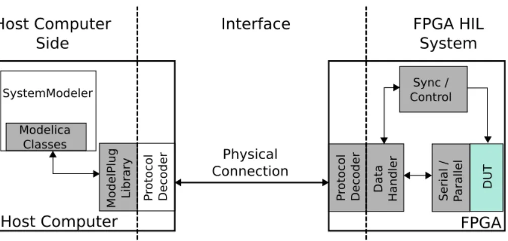
The solution proposed in this thesis presents a platform based in an FPGA to per-form hardware-in-the-loop simulations. The system has three main components: The host computer with the simulator, the FPGA board, and a communications interface. To clarify the purpose of these components, a comparison with the common HIL set up explained in chapter 2.2, and especially with image 2.2, can be done. The first element, the host computer that includes SystemModeler sim-ulator, will contain the HIL model. Then, SystemModeler, with the help of the interface, provides the simulated sensors to the DUT which is implemented in the FPGA. Thereafter, when the DUT in the FPGA has produced a response, this response is sent back to SystemModeler using the interface. Additionally, if there are test cases for the simulation, these can be implemented in SystemModeler as well.
16 3 System design ModelPlug Library Modelica Classes Sync / Control DUT Physical Connection
Host Computer FPGA
P
rotocol Decoder Protocol Decoder
SystemModeler FPGA HIL System Interface Host Computer Side Data
Handler Serial / Parallel
Figure 3.1:High level schematic of the elements of the system.
Figure 3.1 contains a more detailed explanation of the different elements of the proposed platform. The figure shows all the components of the platform, how-ever, during this thesis there were only created the elements coloured in Grey. Additionally, two examples are presented in this thesis for the DUT, light blue on the picture. The following sub-sections contain a description of these elements and their purpose.
3.1.1
Host computer
The first part on figure 3.1 is the host computer. The main element in this side is the SystemModeler simulator; SystemModeler’s main purposes are to create the simulation model, control the simulation flow, and display the results. The prob-lem then is how to represent the FPGA, or the DUT, in this simulation model. To solve this, a group of classes written in Modelica are used. These classes repre-sents the FPGA, the inputs, and the outputs of the digital design. These classes proportionate additionally a good platform to modify the configuration parame-ters for the simulation. Once the DUT is represented in the simulation model, this representation has to be connected with the actual DUT implemented inside the FPGA. The ModelPlug library, the second biggest element on the host computer side, is in charge of this connection; it prepares the simulation data and creates the transmission data packets. Lastly, an issue arises with the use of different languages. SystemModeler uses Modelica language and ModelPlug is written in C++. Therefore, a group of extern C functions are used. Modelica supports to call extern C functions, so SystemModeler invokes these functions which in turn invoke their counterparts in ModelPlug to perform the final communication. The work during this thesis in this side of the platform regarded the creation of the Modelica classes, the ModelPlug library based on a previous existing model of ModelPlug, and the extern C functions.
3.1.2
Interface
The interface is the second main block of the proposed system, it creates the con-nection between the FPGA HIL system and the host computer. It is represented in figure 3.1 between the ModelPlug library and the FPGA HIL system. A normal interface is composed by a physical connection and two protocol decoders, one on each side of the physical connection.
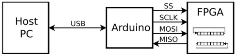
In this thesis the SPI protocol has been used for the interface. However, the host computer is not able to produce this SPI protocol, therefore an Arduino board is used. The software protocol decoder placed in the host computer transmits using the USB serial port of the computer to the Arduino. Thereafter, the Arduino transforms that transmission to the SPI protocol and sends it to the FPGA. In the FPGA side the second protocol decoder block is implemented and is used to read this SPI transmission.
The work in this side of the platform during this thesis consisted in the creation of the hardware protocol decoder in the FPGA and the programming of the Arduino board.
3.1.3
FPGA HIL
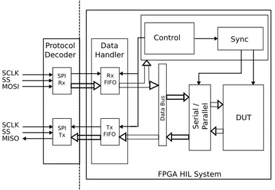
The third element shown in figure 3.1 is the FPGA HIL system, this element contains the DUT that is simulated. The purpose of the FPGA HIL system is to prepare the data signals for the DUT and to control the simulation run time in the FPGA. To be able to perform this, the FPGA HIL system is composed by five blocks: A data handling block, a control block, a synchronization block, a serial-parallel block and the DUT. A schematic with the composing blocks of the system is shown in figure 3.2.
In figure 3.2 all the components implemented in the FPGA are represented. It includes the protocol decoder, which is in fact part of the interface, the DUT, and the FPGA HIL system. In the following paragraphs the data flow through the FPGA will be followed to explain the different components.
The first block in the FPGA that receives the information from the interface is the hardware protocol decoder. As explained before this block is used to recover the incoming SPI signal and sends it to the data handler block.
The second block, the data handling block, has three main purposes: First, to store the data samples until they can be processed. Second, to make the FPGA HIL system more independent from the interface used. This is obtained by only allowing this block to interact with the interface and minimizing the connections of the data handling block with the interface. The third purpose is to perform data synchronization; the FPGA and the SPI decoder use different clock domains that need to be synchronized.
18 3 System design Data Bus Control Sync DUT Serial / Parallel Rx FIFO Tx FIFO SPI Rx SPI Tx Protocol Decoder Data Handler
FPGA HIL System
SCLK SS MOSI SCLK SS MISO
Figure 3.2:Schematic of the FPGA system. White arrows represent data flow and black arrows represent control signals
The next block in the data flow is the control block. The control block is in charge of reading all the commands sent by the software simulator and setting the start of the simulation inside the FPGA. When a new transmission arrives, the control block reads the first data value, which is an operation command, and sends the corresponding control signals to the rest of the system.
The following block is the synchronization block. To run the DUT each sampling period in the FPGA needs of three main phases: The load of the data, the run of the time step, and the acquisition of the results of the current sampling period. The synchronization block is in charge of processing these three phases at the correct moment.
The lasts two blocks in figure 3.2 are the serial-parallel block and the DUT it-self. The purpose of the serial-parallel is to provide the inputs for the DUT to simulate. Most of HW designs are composed by several inputs or outputs, there-fore, the need for this block is due to in the necessity of transforming the serial communications to this parallel nature. This block can be divided itself into two smaller sub-blocks: A serial-to-parallel block that performs that transformation at the input of the DUT and a parallel-to-serial block at the output of the DUT. The whole FPGA side of the platform has been created during this thesis. For the DUT, two examples are provided in chapter 5.
3.2
Specific requirements for the design components
This section explains how the main requirements, explained in section 1.2, affects the different components of the proposed solution.The major requirement regarding the host computer part of the thesis is the us-ability of the system because SystemModeler is the main element that the user will interact with. The process to create and use a new simulation model needs to be simple; simple to understand from a user point of view how the DUT in the FPGA is represented in the simulation model and how to configure it. Addition-ally, the general requirement concerning the data types is important in the host computer. The ModelPlug library is in charge of all the data transformations that are needed for the HIL platform. Moreover, the configuration of these data types needs to be straightforward for the user.
For the interface, requirement number five in section 1.2 is important: The inter-face should be available for most FPGAs in the market. Since the proposed plat-form targets a wide range of users, the interface needs to be highly compatible. On the host computer side, the interface should not have compatibility problems with different OS. This is also important taking into account that SystemModeler works for Windows, Linux, and Mac. Additionally, the interface should be rela-tively simple to implement in a new FPGA design. Another basic consideration for an interface is the communication speed. For use of the co-simulator, the transmission speed is important, but for uses as a co-processor the communica-tion speed is critical. However, most high-speed interfaces are not available for low or medium end FPGAs, which enters in conflict with the first requirement for this part of the design.
The requirements that concern the FPGA side are based on the flexibility of the platform. First, the FPGA HIL system that controls the simulation of the DUT needs to occupy the smallest area possible. This is necessary to widen the range of FPGAs that can be used for the HIL platform. Second, the system has to be flexible with the DUT architecture. Digital designs that can be implemented as DUTs does not have a fixed architecture (they vary on degree of parallelism, num-ber of inputs/outputs, size or type of those inputs/outputs). The platform needs to adapt to the different architectures that digital designs can have. Moreover, it should be simple, from the user perspective, to configure the FPGA platform for different DUT architectures. Third, the FPGA system needs to be designed in such a way that the implementation of new functionality is simplified. The pro-posed solution is a first version of a HIL platform for SystemModeler, therefore the platform should allow to implement new functionality in the future.
4
Design implementation
This chapter contains a more detailed explanation of the technical implementa-tion of the different parts of the design. This chapter is divided in three main sections: The first one contains the explanations of the host computer side of the thesis, the second section on the interface, and the third and last section on the FPGA HIL system.
4.1
Host computer
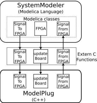
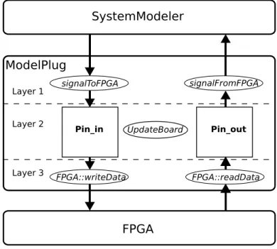
The work in the host computer side involved mostly the modifications of the ex-isting ModelPlug library and the connection of this library with SystemModeler through three Modelica classes. Figure 4.1 shows the schema of the interaction between the host computer elements. The two main elements shown in the fig-ure are the simulator SystemModeler and the communication library ModelPlug. The third element shown in the figure are the extern C functions. As explained in the previous chapter, these functions are used to interconnect the Modelica code from SystemModeler with the C++ code of ModelPlug. The three Modelica classes in SystemModeler call their respective extern C functions which in turn call the ModelPlug C++ functions. In the figure the direction of the data transmis-sions between the functions is depicted with the arrows. Actual simulation data is sent to and from the FPGA with the SignalToFPGA and SignalFromFPGA groups of functions. The group of functions of updateBoard are used to trans-mit configuration data and actualize the sampling periods.
22 4 Design implementation
SystemModeler
(Modelica Language) Modelica classes Signal To FPGA Signal From FPGA FPGA Extern C Functions Signal From FPGA Signal To FPGA update Board update Board Signal To FPGA Signal From FPGAModelPlug
(C++)Figure 4.1:Representation of the interaction between the host computer el-ements.
4.1.1
Modifications in SystemModeler
The main purpose of the SystemModeler side is to create the simulation environ-ment and control the simulation. The simulation model in Modelica is performed interconnecting blocks that represent the different functionality. Therefore, some of these blocks have to be created to represent the DUT implemented inside the FPGA board in the simulation. These blocks are the three Modelica classes cre-ated in SystemModeler; these classes are shown in image 4.2 and represent the FPGA itself, the inputs, and the outputs of the DUT.
Pin 0
Out
FPGA
/dev/ttyACM0 Pin 0
In
Figure 4.2:Diagram representation of the three SystemModeler classes. Additionally, these classes can be used for two additional purposes: To call the extern C functions previously mentioned and to define the configuration param-eters for the host computer.
FPGA class
The first class created is the FPGA board. This FPGA board class is implemented inside a bigger class that comprehends the different boards that ModelPlug al-lows to connect. This class is additionally used to call the updates for the data samples at every sampling time. In other words, when a sampling point is reached the FPGA board class starts the updateBoard functions that will actualize the simulation values to send to the FPGA.
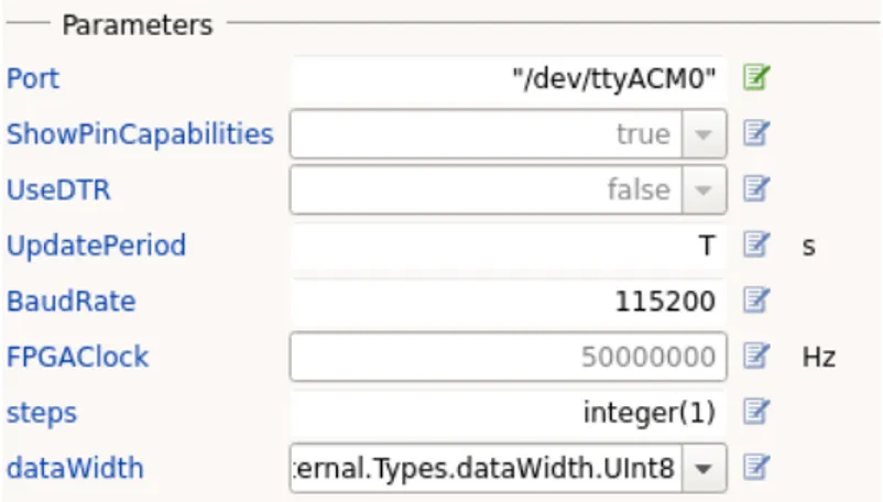
Figure 4.3:Configuration parameters for the FPGA class.
Regarding the configuration parameters for the FPGA class, an image of them is shown in 4.3. The configuration parameters for this class are:
1. The communication port that SystemModeler is using. During this thesis the communication ports in the host computer side are serial ports.
2. The showPinCapabilities parameter is not used for the FPGA commu-nication. The version of ModelPlug for the FPGA created during this thesis does not take care of them.
3. The useDTR is not used either for the FPGA communication.
4. The sampling period specifies how often the communications with the FPGA board are performed using the updateBoard function.
5. The baud rate used for the communications. This baud rate is used for the serial communication in the host computer side.
6. The internal FPGA clock frequency in Hz.
7. The number of time steps to run inside the FPGA board. This number of time steps is specified in clock cycles. By define the value used is the sam-pling period.
24 4 Design implementation
8. The data width used inside the FPGA and in the interface. However, this parameter does not actually set the data width inside the FPGA (this is performed by other parameter specified in a VHDL package in the FPGA system code), this parameter is used only for configuration purposes in the host computer side.
Input and output port classes
The second group of classes created represent the inputs and outputs of the DUT. They are calledsignalToFPGA and signalFromFPGA and are homonym to their
corresponding functions in ModelPlug and in extern C. They are used to send and receive data to ModelPlug every sampling interval after the stored values are updated by updateBoard.
Figure 4.4:Configuration parameters for the input and output classes.
These two classes have three different configuration parameters, shown in figure 4.4:
1. The pin number, which only function is to order the inputs and outputs in the software side of the platform. The input and output pins are sent through the interface from the smallest to the biggest. This means that the pin numbers have to be set accordingly with the architecture of the DUT. 2. The signalType is used to determine the data type that will be sent to
the FPGA. The parameter specifies both the word length of the signal (it accepts 8, 16, 32, and 64 bits) and if it is signed or unsigned.
3. The number of fractional bits the number has. However, if the number is an integer, setting this parameter to 0 is enough.
The main purpose of these configuration parameters, especially the second and the third, is to define the data types used in the FPGA.
4.1.2
ModelPlug
Once the simulation model is created and the configuration parameters for the software have been defined in the SystemModeler side, the problem left is to or-ganize these configuration parameters and the data samples so the FPGA HIL sys-tem can understand them. The communication from ModelPlug to the FPGA is performed with unsigned data packets of a fixed size, therefore the data received from the simulator needs to be translated in this library. Additionally, as com-mented in section 3.2 the FPGA side needs to receive the operation commands from the host computer, these operations commands are created in this library. The communications performed by the ModelPlug library can be divided in three layers. A top layer that interacts with SystemModeler, a medium layer that op-erates with the data, and a low layer that interacts with the serial interface. A diagram of this layer implementation is shown in figure 4.5.
Layer 1 Layer 2 Layer 3
SystemModeler
UpdateBoardFPGA
signalToFPGA signalFromFPGA FPGA::writeData FPGA::readDataModelPlug
Pin_in Pin_outFigure 4.5:Communication layers of ModelPlug.
The centre of the design of the ModelPlug library are two buffers: pin_in and pin_out. These buffers are used to store the values of the data signals for, re-spectively, the input and the output. Those buffers are accessed to store or read data by the top layer and the medium layer of the ModelPlug library.
In this subsection only the functions of the ModelPlug library that have been created or highly modified during this thesis are explained.
26 4 Design implementation
Top layer
The top layer of ModelPlug acts as an intermediary between SystemModeler and ModelPlug. These functions, that are called signalToFPGA and signal-FromFPGA, are used to solve the data type differences between the simulator and the FPGA. The simulator side uses floating point data types meanwhile the most common in the FPGA designs are fixed points data types. This data transforma-tion is performed in three phases:
1. The incoming signed data samples of type double are multiplied with
2no. of decimals, in this way the resulting value is the original scaled with the
number of fractional bits desired.
2. The resulting sample is stored in a uint64_t data type, type that is used in the ModelPlug library. The conversion to uint64_t is done using pointer referencing1to store the information bits of the data samples. In this way, the sign is saved even if the data type used is an unsigned like uint64_t. 3. The converted uint64_t data sample, already with the information in
fixed point values, is stored in the pin_in buffer for the next layer to use. The three steps are very similar for the data received from the FPGA, they are however inverted:
1. The data received is already stored in the pin_out buffer, but this data is stored as uint64_t so the sign needs to be recovered. The samples received are stored in uint64_t types even though they contain actual signed data. To recover a signed value stored in an uint64_t data type the function needs to: First, know the real size of the sample. This is because the function needs to take the correct bits of the uint64_t sample, includ-ing the sign bit, and discard the rest. Second, perform pointer referencinclud-ing, in a similar way that in the sent data, to recover the sign.
2. Once the data sign is recovered the sample is divided by the
2no. of decimalsto scale down the values. This scaled down value is stored in a
double data type, hence recovering the floating point fractional values that SystemModeler uses.
3. The last step is to send these recovered data samples, using the external C functions, to the SystemModeler simulator.
1First, the signed double value is stored in an int64_t sample. Second, an int64_t pointer is created
pointing to the address of new int64_t sample. Third, a second pointer, in this case unsigned uint64_t, is created referencing to the first pointer. Fourth, the last step is to create a uint64_t variable were is stored, using the second unsigned pointer, the original double value. In this way the original signed value is stored in an unsigned variable.
Intermediate layer
The intermediate layer contains the pin buffers and the updateBoard function. This updateBoard function is invoked by the simulator every time the simula-tion reach a sampling point. The updateBoard funcsimula-tion is used to: First, actual-ize the information contained in the pin buffers every sampling period. Second, prepare for the lowest layer the data contained in these buffers. An extra thing that needs to be taken into account is the size of the packets that the interface can handle (for example, the SPI interface uses packets of size either 8 or 16 bits). The updateBoard function divides the total sample to smaller packages of the interface size by shifting the original value. Afterwards, these values are stored in a temporal array, and sent to the lower layer.
The stages for sending data to the lower layer are:
1. Every time a sampling time point is reached in the simulation, update-Boardis invoked and it reads the information stored in pin_in.
2. The values read from pin_in are divided into smaller packets and stored in a temporal array.
3. This temporal array with all the packets for all the inputs is sent to the low layer of ModelPlug.
The stages for receiving data are the same but inverted in order:
1. A temporal array is received from the low layer with all the packets for all the FPGA outputs.
2. The packets are joined together by shifting.
3. The buffer pin_out is actualized with the new values for the output pins of the FPGA.
28 4 Design implementation
Low layer
The last layer, the lowest one, includes the functions that interact directly with the interface. They are called by updateBoard every sampling point to send and receive the signals from the FPGA. Their main function is to build the trans-mission packet. This transtrans-mission packet is shown in figure 4.6.
Operation (OP) Size (S) Data Packet (D) Data Packet (D) Data Packet (D) Data Packet (D) Header Header Data
Figure 4.6:Composition of the transmission packets.
The transmission packet consists in a header and the data. The data is composed by the data packets provided by the intermediate layer. The header is constituted by the operation commands and the size of the transmission. The operation com-mands are used to tell the FPGA which functionality to perform, the current operations are: writeData, readData, writeTstep, and resetFPGA.
writeData Operation command used to send data to the FPGA. The operation code used is 0x5A for transmission packets of one byte length. If the trans-mission packets are longer than one byte, the operation code is extended. After sending this operation code are sent the size and the data packets received from updateBoard.
readData Operation command used to receive data from the FPGA. The opera-tion code in this case is 0x55. The host computer, that is the master in the synchronization mode used, sends the operation command and the size of the transmission to the FPGA. Thereafter, the FPGA answers by sending the data packets.
writeTstep This is a configuration command with a operation code of 0x56. It is used at the beginning of the simulation to configure the Tstep, or in other words, to configure how many clock cycles has to run the DUT during each simulation iteration.
resetFPGA Operation command used to reset the FPGA from the host computer. The operation code for this command is 0x51.
These operation commands are created with different functions, one for each of them, in the low layer. These functions are called by updateBoard and use the pin buffers to store or take the information.
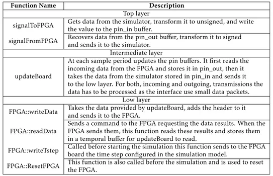
A summary of the functions used in the ModelPlug library is shown in table 4.1. The functions in this table are ordered by communication layers.
Table 4.1: Summary of the functions used in ModelPlug, ordered by com-munication layers.
Function Name Description Top layer
signalToFPGA Gets data from the simulator, transform it to unsigned, and writethe value to the pin_in buffer. signalFromFPGA Recovers data from the pin_out buffer, transform it to signed
and sends it to the simulator. Intermediate layer
updateBoard
At each sample period updates the pin buffers. It first reads the incoming data from the FPGA and stores it in pin_out, then it takes the data from the simulator stored in pin_in and sends it to the low layer. For both, incoming and outgoing, transmissions the data has to be processed as the interface use small data packets.
Low layer
FPGA::writeData Takes the data provided by updateBoard, adds the header to it and sends it to the FPGA.
FPGA::readData
Sends a command to the FPGA requesting the data results. When the FPGA sends them, this function reads these results and stores them in a temporal buffer for updateBoard to read.
FPGA::writeTstep Called before starting the simulation this function sends to the FPGA board the time step configured in the simulation model.
30 4 Design implementation
4.2
Interface
The interface comprises the physical connection between the FPGA and the host computer and the modules that decode the signals. Three main possible connec-tions have been studied for this thesis: The USB JTAG, Ethernet and SPI. The last one, SPI, has been finally chosen for this thesis. This decision has been done be-cause the SPI is a simple interface that could be connected to the GPIO port of the FPGA and could average a similar speed that the USB JTAG. An additional benefit of using this transmission in the host computer side is that they do not require additional drivers, so it is possible to use them in any computer with any operative system. The design on the FPGA board would allow to implement a dif-ferent interface without many changes, although, some interfaces like Ethernet may need a soft-processor to be able work. The library ModelPlug is designed to use serial communications such as USB, so the implementation of some interfaces like Ethernet would need to modify the library.
4.2.1
SPI
Theory
The chosen interface for the proposed solution is the Serial-Parallel-Interface (SPI). This is an interface that uses four wires and sends the data bits in se-ries. The wires used are a SPI clock wire (SCLK), a chip select wire (SS), and two data wires one for each direction: Master-Output Slave-Input (MOSI), and Master-Input Slave-Output (MISO).
SS SCLK MOSI MISO Z Z bit 1 bit 1 bit 2 bit 2 bit 3 bit 3 bit 4 bit 4 bit 5 bit 5 bit 6 bit 6 bit 7 bit 7 bit 8 bit 8 Z Z
Figure 4.7:SPI communication protocol for mode 0.
An example of a SPI communication is shown in figure 4.7. The bits are sent in series, one by one, through MOSI or MISO depending of the direction of the transmission. The bit rate of the transmission is controlled by the SCLK and each bit is sent in one pulse of this clock. The SPI connection is a master-slave connection, in which one master can control several slaves at the same time. The chip select wire controls which of those slaves is being targeted at the moment. The SPI communication has three modes depending on which polarity, phase and edge of the SPI clock are used. For the case implemented in this thesis, the mode used is mode 0 with transmission of the most significant bit first. This is the mode
represented in figure 4.7. In it the SPI clock has a polarity of zero, which means that the active state is one and the inactive is zero. Moreover, the clock phase for this mode is also zero which means that the sampling of the data is done in the rising edges of the clock and the data has to be outputted on the falling edges of the clock.
Implementation
A normal computer lacks the output interface needed to generate the four wire protocol used by the SPI, therefore to solve this issue an Arduino board is used [32], more specifically a Teensy board [33]. The host computer sends the data signals to transmit to the Teensy board through USB and this board translates it to the SPI protocol. A schematic for this set up is shown in figure 4.8. The physical connection is performed using the dedicated SPI pin interface of the Teensy board together with the GPIO port of the FPGA board.
FPGA
SS SCLK MOSI MISO USBHost
PC
Arduino
Figure 4.8:Schematic for the interface set up for the SPI connection.
In the Teensy side, the transmission packets with the array of data samples cre-ated by the ModelPlug library are received. Then, the function of this board is to transform this information to the SPI protocol shown in figure 4.7 and transmit it through the four SPI wires. For this purpose the Teensy SPI functions, based on the Arduino SPI functions [34], are used. The voltages used are in the 3.3V range for both the FPGA and the Teensy board. However, in case the FPGA had a output voltage of 5V, the Teensy boards have an input tolerance for that. As com-mented before, the Arduino SPI libraries allow to send data samples in sizes of 8 or 16 bits. For this reason the transmission packet is divided in smaller packets of that size by ModelPLug.
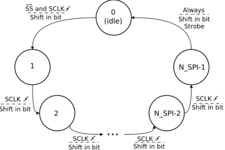
Inside the FPGA a decoder is used to read the SPI protocol and send the data sig-nals recovered to the rest of the FPGA system. This block is divided in two main sections, one for the receiver and another one for the transmitter. The incoming and outgoing bits are stored in two shift registers during the transmissions. The control of the transmission has been implemented using finite state machines, one FSM for each of them. Both FSMs are designed with a non-predefined num-ber of states. The numnum-ber of states is defined instead by the parameter N_SPI, which is the number of bits of the data packets. Additionally, the FSMs are con-trolled by the SPI clock not with the FPGA system clock.
32 4 Design implementation
...
0 (idle) 1 2 N_SPI-2 N_SPI-1 Shift in bit Shift in bit Shift in bit Shift in bit Strobe SS and SCLK SCLK SCLK SCLK SCLK Always Shift in bit Shift in bitFigure 4.9: Schematic diagram for the receiver FSM. The state is defined inside the circle. The change of state conditions and the outputs are defined over the arrows.
Receiver FSM The receiver state machine is N_SPI states long, from state 0 to state N_SPI - 1. Figure 4.9 shows a diagram for this FSM. The states are used as a counter for the number of bits that arrive. In each of the states a bit is shifted through the less significant bit position of the shift register. The first state, the state 0, is used as an idle state where the FSM waits until the bit transfer starts. This start is signalled by the first SPI SCLK cycle arrival. Then from state 1 to N_SPI-2 the FSM keeps registering the incoming data bits in the shift register. When it is turn for the last state, state N_SPI-1, it means that the last bit is received so the FSM gives an strobe signal to indicate that the reception is finished. Then, this strobe or ready signal alongside with the data stored in the shift registered are sent to the rest of the FPGA system.
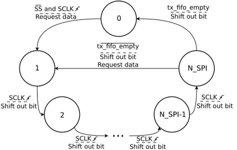
Transmitter FSM The transmitter state machine needs more functionality than the receiver one. This is because the data sample to transmit needs to be loaded in beforehand. A diagram with this FSM is shown in figure 4.10. The total num-ber of states is N_SPI+1. Similarly than with the receiver, the states are used as a counter for the bits to transmit. The state 0 is, similarly to the receiver FSM, an idle state that waits to the first transmission. This first transmission is con-trolled from the FPGA system and is set when the command code for transmit-ting (readData) is received from the host computer. When this code is received the FSM changes to the state 1, which is used to get the data from the FPGA and to wait until the transmission starts. The transmission start is marked when the SPI SS is low and the SPI SCLK starts working. The states from 2 to N_SPI-1 work in a similar way than the receiver, they shift the most significant bit from the shift register to the SPI MISO wire. Then, the last state, N_SPI, shifts the last bit and decides either going to idle or to the state 1 to wait to send more data.
...
0 1 2 N_SPI-1 N_SPI Request dataShift out bit
SS and SCLK
SCLK
tx_fifo_empty
Shift out bitSCLK Shift out bit
SCLK
Shift out bit SCLK Shift out bit
tx_fifo_empty Shift out bit Request data
Figure 4.10:Schematic diagram for the transmitter FSM. The state is defined inside the circle. The change of state conditions and the outputs are defined over the arrows.
Two points more to clarify about the interaction of the SPI block with the rest of the system are:
1. The only iterations needed between the SPI block and the FPGA system are the data buses (both for transmit and receive), a request data and a data is ready signals, respectively, for the transmitter and the receiver. This attempt to limit the interactions between the interface block and the rest of the FPGA system is done to reduce the amount of work to change the SPI interface block to another one.
2. The data length used for the interface transmission will define the size of the data width for the FPGA system. The purpose of this, is to simplify the control block in the FPGA. Thus, for the SPI interface case the data lengths of one or two bytes used by the interface would force the FPGA system to use the same ones.
34 4 Design implementation
4.3
FPGA system
The FPGA HIL system is constituted by four elements: Data handling, control, synchronization, and serial-to-parallel conversion, plus the DUT to simulate. Ad-ditionally, in the source code is given a VHDL file that contains the configuration packages and parameters needed to build the system. Figure 4.11 (showed also in the previous chapter) depicts the design inside the FPGA. The following sub-sections will follow the data flow inside the FPGA HIL system to explain the implementation and configuration of the constituent elements.
Data Bus Control Sync DUT Serial / Parallel Rx FIFO Tx FIFO SPI Rx SPI Tx Protocol
Decoder HandlerData
FPGA HIL System
SCLK SS MOSI SCLK SS MISO
Figure 4.11: Schematic of the FPGA system. White arrows represent data flow and black arrows represent control signals
4.3.1
General parameters
The configuration of the DUT file is unknown when the FPGA HIL system is designed. Therefore, the design of the HIL system needs to be created in a generic manner that can be parameterized. For this purpose there are three main groups of parameters used to build the system. Those parameters are set as constants in a package called config_pkg located in the same working library as the rest of the files. This package needs to be invoked in every VHDL file for successful synthesis.
The parameters defined in this package that are used for the system configuration are:
1. The interface word length, its generic name is data_width. This parame-ter is used to build the data word length of all the system.
2. The number of inputs and the number of outputs, called respectively N_in and N_out. These two numbers are used to generate the input and output registers in the serial-to-parallel block.
3. The data lengths for each input and output. These parameters are config-ured as an array with the sizes of each individual input or output. The array names are size_array_in and size_array_out. These values are used as well in the serial-to-parallel block to generate the the input and output registers.
Each individual element of the FPGA uses these configuration parameters during synthesis to create the system for each individual DUT simulation.
4.3.2
Data handling
The data handling block is the first element of the FPGA HIL system seen from the interface side. As commented in section 3.1.3, the two main purposes for this element are to store the incoming and outgoing data from the FPGA and to make the FPGA system more independent from the interface. An additional issue that this block needs to solve is the crossing of clock domains, the interface works with a different clock domain that the rest of the FPGA.
To address these purposes are used asynchronous FIFO memories. The use of asynchronous FIFO memories allows to maintain reliable communication bet-ween, two clock domains, while maintaining a faster data rate than the managed with other techniques such as handshakes. The final design consists in two FIFO, each of them with one reading port and one writing port. Those ports works independently, therefore there are needed two address registers for each mem-ory. The control of these FIFOs’ addresses is internal in the data handling block, which simplifies the implementation of a new interface decoder without modify-ing this block. The implementation of the FIFOs is done usmodify-ing dual port RAMS together with the write and read logic. A diagram for the data handler block design is shown in figure 4.12, in the figure the FIFO on top is the FIFO for the interface receiver and the FIFO under that is for the interface transmitter. The FIFOs behaviour is controlled mostly inside the data handling block itself. For the writing of both FIFOs are only needed two external signals: A data_ readysignal high during one clock cycle and the data signal itself. In a similar manner, for the reading of the FIFOs, two signals are needed: A read_data one clock cycle signal and the data signal. When read_data is asserted the FIFOs will read and set the new value at the data output. An additional signal, named