ECOLOGICAL TECHNOLOGY AND MANAGEMENT KALMAR,SWEDEN, September 22-24, 1999
10
POLARIZATION
PHOTO ABSORPTION
SPECTROSCOPY OF
ZnO/CdS/Cu(In,Ga )Se
2THIN FILM SOLAR CELLS
Vasi/ii Yu. Rud'
St Petersburg State Technical University, Russia
ABSTRACT
The photosensitivity of polycrystalline-film Cu(ln,Ga)Se2/CdS/ZnO solar cells
with different thickness of CdS and ZnO films have been studied. These
structures exhibit a conversion efficiency 11-12% in the spectral region from 1.2
to 2.4 eV at T= 300 K. Polarization photosensitivity was observed for oblique
incidence of linearly polarized light on the ZnO surface of these structures. The
induced photopleochroism and an increase of the photocurrents as a result of a
decrease of reflection losses were found. The induced photopleochroism
8
2coefficient P1
increases with the angle of incidence E> as P1
-and its value is
found to be 10-17% at E>= 75e
°. The results of these polarization investigations
demonstrate the sensitivity of the photoelectric processes to the optical quality
of the ZnO films. Such polycrystalline-film solar cells can be employed as
polarization-photosensitive devices.
KEYWORDS
Introduction
Chalcopyrite-type semiconductors such as CulnSe2 and their quaternary and pentenary solid solutions have been attracted an attention for their large absorption coefficients and the desirable band gaps for photovoltaic energy conversion. Polycrystalline Cu(ln,Ga)Se2 film has emerged as an important material for high efficiency, stable, and radiation hardness thin film solar cells (Stolt et al., Schmidt et al., Ruckh et al.). Thin film solar cells with active area efficiencies in the range of 15-18% have been fabricated on such absorber films (Stolt et al.). In this paper we report the results by the polarization photoabsorption measurements of Cu(In,Ga)Se2 solar cells prepared with varyous thickness of CdS and ZnO films.
Experimental methods
In our investigation we used Cu(In,Ga)Se2 - based thin film solar cells produced in Germany ( Stuttgart University ). It is based on a Cu(ln,Ga)Se2 absorber film and ZnO window film ( serving as a transparent top contact ), which are
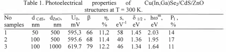
Table I. Photoelectrical properties of Cu(ln,Ga)Se2/CdS/ZnO
structures at T = 300 K. No d CdS, dzno, Uo,
�
l], s, o 112, hwm , P1, samples nm nm mV % eY-1 eV eV % 1so
500 595,3 66 11,2 58 1.45 2.03 14 2 100 500 595.6 68 11.4 40 1.36 1.95 17 3 100 1000 619.7 79 12.2 46 1.34 1.64 11separated by a thin CdS buffer window film. A Mo back electrode is DC-magnetron sputtered on glass plate. The fabrication of Cu(In,Ga)Se2 absorber films proceed by multisource sputtering. The composition of the solid solution corresponded to the ratio In/(In+Ga)=0.25 and was chosen on the base of the requirements which must be met in order to obtain higher photoconversion efficiency. Next, a CdS buffer film was grown using chemical bath deposition and then a ZnO film was grown using RF-sputtering. The thickness of ZnO and CdS films in thin film solar cells are given in Table I.
In all experimental results given below, the structures was illuminated through the top film by natural and linearly polarized radiation ( LPR ). To determine the polarization parameters of the solar cells photosensitivity were secured in a STF-1 (the Fedorov's table in Russian), which made it possible to vary continuosly the angle of incidence 0 of the radiation on the receiving surface and the azimutal angle <p between the electric vector E of the light wave and the plane of incidence of the radiation ( PIR ). The photosensitivity of the solar cells was measured in the regime of a short-circuit photocurrent, which was proportional to the flux density of the incident radiation, making it possible to determine the relative photoconversion quantum efficiency l] as the ratio of the photocurrent to the number of incident photons. The spectral resolutions of the setup was no worse than I meV.
I.-•
3.0
ECOLOGICAL TECHNOLOGY AND MANAGEMENT KALMAR,SWEDEN, September 22-24, 1999
Results and discussion
1I..1--5,· _____ �-�...
The photoelectric parameters for thin film devices with different� 1 ___ 2.4 ... _, 3.1
I thickness CdSiC
·-..1
..
( d eds ) and ZnO ( d zno ) films are1
'
presented in Table I. As follows fromI Table 1, the maximum open-circuit
2.35
photovoltage U0 , fill factorp,
and: 1.17
-·-·- '
photoconversion quantum efficiency 11•--- are attained at d zno = 1000 nm.
I.
,,
\
'
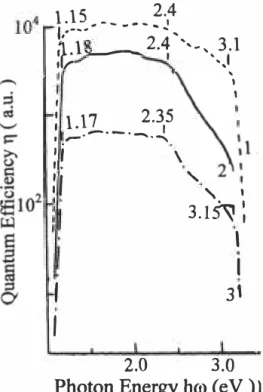
Fig. 1 shows the spectral dependences ofI
:
,
'3.1�:
'
'
I
31
I
the relative quantum efficiency for these structures at T = 300 K. When such structures are illuminated in the direction of the normal to the surface of ZnO film, the window effect, typical for all devices, was observed.
2.0
Photon Energy hro ( e V ) )
Fig. l: Room-temperature spectral dependences
of the TJ of Cu(In,Ga)Sei/CdS/ZnO structures
( Numbers by curves correspond to Table l ).
Here the long-wavelength photosensitivity limit obeys an exponential law and is localized in the region of photon energies corresponding to the band edge absorption in a Cu(In,Ga)Se2 film . It is characterized by a slope s from 40 to 58 eV-1 for the different photoconverters ( Table I ), which is typical for direct interband A-transitions. The short-wavelength limits of the photosensitivity is caused by the appearance of interband absorption in a CdS ( hco > 2.35 e V ) and ZnO (hco > 3. I e V ) wide-band films. The full width at half efficiency of the spectral characteristics ,i(hco) is 6 112 = 1.34 - I .45 e V for the different solar cells ( see Table I ) and it characterizes them as a wide-band photoconverters of natural radiation. The energy position of the photosensitivity maxi-mum hcom removes to the long-wavelength region and the 6 112 have the tendency to fall with the increase of the thickness CdS and ZnO films ( Fig. 1 and Table I ).
--\
�
It should also be noted that the interference features in the ri(hco) for the investigated solar cells in contrast to (Rud' V. Yu. et al.) are not observed . Probably it is connected with lowering of the quantum efficiency on investigate structures relatively (Rud' V. Yu. et al.).
When the obtained solar cells
to
were illuminated by linearly/ 0 --- polarized radiation in a direction
o normal to the plane of the ZnO
1 /
\
film their short-circuit�,o-o
200
...
f
--....,
20
photocurrent i was independentof the spatial orientation of the .••••.✓--� 2
60
''
�
-
0 electric vector E of the light\
�-
-
'
\-
�
the polarization indicatrix of the wave. Therefore, when 0 = 0°,
photocurrent iq, degenerates intoa straight line. This is
s
�
-�
determined by the isotropiccharacter of the photoactive absorption in the polycrystalline ZnO, CdS, and Cu(In,Ga)Se2
8 100
10
films. As a result, the induced photopleochroism coefficient A P1= ( / - is ) II
(/+is ) , (1)3/
,,.
_/
A
01....-::::: ,
10
0
I
90
Incidence Angle 0 ( deg. )
Fig. 2: Angle of incidence dependences of
i
sthe photocurrents ( / - 1,
- 2 ) and
induced
photopleochroism
(3)
of
Cu(ln,Ga)Se2/CdS/ZnO structures ( Sample
No 3, A= 0.50
µm).�
ECOLOGICAL TECHNOLOGY AND MANAGEMENT KALMAR,SWEDEN, September 22-24, 1999
where
t
and i
5are, respectively, the photocurrents with E
II
PIR
E
08 10
.c: p.. "O Q) 0o___�__._____..__ _____ .__
1.0
2,0
3.0
Photon Energy hro ( e V )
Fig. 3: Spectral dependences of induced
photopleochroism
of Cu(ln,Ga)Se2/CdS/ZnO structures ( Numbers by
curves correspond to Table 1, 0=75° ).
and E.L PIR , is equal to zero in the entire region of the solar cells photosensitivity. For this
reason, there are grounds for believing that these solar cells do not posses natural
photopleochroism ( Figs. 2 and 3 ) ( Kesamanly et al. ). Switching to measurements of the
photosensitivity of solar cells in a geometry with oblique incidence of LPR on the receiving
plane of the cells, i.e., 0 > 0
° ,
differences appear in the values of the photocurrentst
and is .As a result, the P1 becomes different from zero and increases continuosly with increasing
angle of incidence as a square law P1- 02 . Indeed, as one can see from Fig. 2 , the function
P1 ( 0 ) leaves zero at 0 = 0
°,
which shows that there is no natural photopleo-chroism (Kesamanly et al. ). In the case 0 > 0
°
the photo-pleochroism which apgears is classified,according to ( Kesamanly et al. ), as induced, and in the coordinates ( P1) - hco these curves
are straigth lines in agreement with the analyses ( Medvedkin et al. ) .
The dependences of the photocurrents
t
and is on the incidence angle of the LPR for the examined thin solar cells exhibit a similar behavior over the entire photosensitivity range. The examples of such dependences are shown in Fig. 2. At first, photocurrents for p- and s polarization increase with the 0, then reach a maximum values for each polarization,and only than start to drop rapidly. These features may be connected with the elimination of
the reflection losses for the radiation of each polarizations. Formerly the similar regularity was be found for structures with higher quantum efficiency ( Rud' V. Yu. et al., Rud' V. Yu.).
The induced photopleochroism coefficient on structures with varying thickness of the CdS and ZnO films ( Fig. 3 ) remains virtually constant in the wide energy region from 1.4 to 3 e V
Rud' V. Yu. et al.). An estimate of the refraction index on the basis of value P1 = 10 - 17 % at 0 =75
°
for the different structures with Tl = 11 - 12 % gives n = 1.2 - 1 .4. These values differs from known value of n for ZnO ( Baranskii et al. ). The observed changes of the P1 at hco > I .4 e V may be cause the modifications of anti reflection properties of the examined solar cells. If to take in account the drop P1 ➔ 0 as the antireflection measure ( Botnaryuk et al. ) then the maximum of the enlightenment effect for obtained solar cells was reach at d zno = 1000 nm. Important marked that exactly on this structure obtained the maximum value of the Tl· The fall of thickness ZnO films caused on the decreasing of enlightenment effect and photoconversion efficiency.Summary
Measurements have been made of the photosensitivity of the polycrystalline-film Cu(ln,Ga)Se2/CdS/ZnO structures. These structures exhibit a quantum efficiency 11 - 12 % at T = 300 K. Polarization photosensitivity was observed for oblique incidence of linearly polarized light on the ZnO surface of these structures. The pho-topleochroism was studied as a function of the thickness CdS and ZnO films. The polarization photoabsorption spectroscopy applied to polycrystalline structures show-ed that they can be used in a new function for this type devices -wide-band photo-analyzers of the LPR. It is shown that the induced photopleochroism is sensitive to the quality of the polycrystalline-film structures.
Acknowledgment
ECOLOGICAL TECHNOLOGY AND MANAGEMENT KALMAR.SWEDEN. September 22-24. 1999
List of references
Baranskii P.l. Klochkov V.P. And Potikevich I.V. ( 1 975). Semiconductor Electronics . Naukova Dumka. Kiev.
Botnaryuk V. M. Koval' A.V. Simashkevich A.V. Shcherban D.A. Rud' V.Yu. And Rud' Yu.V. ( 1 997), Polarization photosensitivity of silicon solar cells with an antire-flection coating consisting of a mixture of indium and tin oxides. Semiconductors. 3 1 (7), 677.680. Kesamanly F.P. Rud' V.Yu. And Rud' Yu.V. ( 1 996). Natural photopleochroism in semiconductors -a review. Semiconductors 30( 1 1 ). I 00 1. 1 0 I 0.
Medvedkin G. A. And Rud' Yu. V. ( 1 98 1 ). The parameters of polarization photosensitivity of isotropic semiconductors. Phys. St. Sol.e. 67(a). 333.337.
Ruckh M . Schmid D. Kaiser M. Schaffler R. Walter T. And Schock H.W. ( 1 e996). Influence of substrates on the electrical properties of Cu(ln.Ga)Se2 thin films. Solar Energy Materials and Solar Cells. 4 I /42.335.343.
Rud' V .Yu. ( 1 998). Induced Photopleochroism GaAlAs/GaAs heterophotoelements. 3rd St.
Petersburg Assembly of Young Scientists and Specialists. St. - Petersburg, Russia.
Rud' V.Yu. Rud' Yu.V. Walter T. And Schock H.W. ( 1998). Induced photopleochroism of ZnO/CdS/Cu(In.Ga)Se2 solar cells. Inst. Phys. Conf. Ser. No 1 52,97 1 .974.
Schmidt D. Ruckh M. And Schock H.W. ( I 996). A comprehensive characterization of the interfaces in Mo/CIS/CdS/ZnO solar cells structures. Solar Energy Materials and Solar Cells, 4 1 /42.28e1.294.
Stolt L. And Bodegard M. ( 1 996). High efficiency thin solar cells based on chalcopyrite semiconductors. Cryst. Res. Technol., 3 1 ( I ).397.404.