Horizontal Slot Waveguides for Silicon Photonics
Back-End Integration
MAZIAR A. M. NAIINI
Doctoral Thesis in Microelectronics and Applied Physics
KTH, Royal Institute of Technology
TRITA-ICT/MAP AVH Report 2014:17 ISSN 1653-7610
ISRN KTH/ICT-MAP/AVH-2014:17-SE ISBN 978-91-7595-340-3
KTH School of Information and Communication Technology SE-164 40, Kista SWEDEN A dissertation submitted to KTH Royal Institute of Technology, Stockholm, Swe-den, in partial fulfillment of the requirements for the degree of Teknologie Doktor (Doctor of Philosophy). The public defense will take place on 05 December 2014 at 10.00 a.m. at Sal A, Electrum, Isafjordgatan 26, Kista.
Cover image: Right segment, fabricated photonic chip with double slot high-k waveguides and selectively grown germanium mesas. Top left segment, fabricated embedded graphene photodetector. Bottom left segment, cross section of double slot high-k waveguide.
© Maziar A. M. Naiini, September 2014
Abstract
This thesis presents the development of integrated silicon photonic devices. These devices are compatible with the present and near future CMOS technology. High-k horizontal grating couplers and waveguides are proposed. This work consists of simulations and device design, as well as the layout for the fabrication process, device fabrication, process development, characterization instrument development and electro-optical characterizations.
The work demonstrates an alternative solution to costly silicon-on-insulator photonics. The proposed solution uses bulk silicon wafers and thin film deposited waveguides. Back-end deposited horizontal slot grating couplers and waveguides are realized by multi-layers of amorphous silicon and high-k materials.
The achievements of this work include: A theoretical study of fully etched slot grating couplers with Al2O3, Hf O2 and AlN , an optical study of the high-k
films with spectroscopic ellipsometry, an experimental demonstration of fully etched
SiO2 single slot grating couplers and double slot Al2O3 grating couplers, a
prac-tical demonstration of horizontal double slot high-k waveguides, partially etched
Al2O3 single slot grating couplers, a study of a scheme for integration of the
dou-ble slot Al2O3 waveguides with selectively grown germanium PIN photodetectors,
realization of test chips for the integrated germanium photodetectors, and study of integration with graphene photodetectors through embedding the graphene into a high-k slot layer.
From an application point of view, these high-k slot waveguides add more func-tionality to the current silicon photonics. The presented devices can be used for low cost photonics applications. Also alternative optical materials can be used in the context of this photonics platform.
With the robust design, the grating couplers result in improved yield and a more cost effective solution is realized for integration of the waveguides with the germanium and graphene photodetectors.
Keywords: silicon photonics, slot waveguides, grating couplers, CMOS
tech-nology, high-k, ALD, germanium photodetectors, graphene photodetectors, pho-tonic integrated circuits.
Maziar A. M. Naiini, mamn@kth.se Integrated Devices and Circuits, School of In-formation and Communication Technology, P.O. Box 229, SE-16440 Kista, Sweden
Contents
Abstract iii
Contents iv
Acknowledgements vii
List of Publications ix
Summary of Appended Papers xi
List of Symbols and Acronyms 1
1 Introduction 3
1.1 Why Silicon Photonics ? . . . 3
1.2 Previous Work in Silicon Photonics . . . 5
1.3 Proposed Solution for the Limitations of SOI photonics . . . 6
1.4 SOI Integrated Photodetectors . . . 8
1.5 Proposed Novel Intgration Schemes . . . 11
1.6 Thesis Outline . . . 12
2 Theoretical Models and Experimental Conditions 13 2.1 Finite Element Wave Simulations . . . 13
2.2 Measurement Setup Features . . . 18
2.3 Thin Film Characterization Techniques . . . 24
3 High-k Slot Grating Couplers 27 3.1 Fully Etched Grating Coupler Design . . . 27
3.2 Novel Partially Etched Coupler Design . . . 29
3.3 Double Slot Vs. Single Slot Waveguides . . . 30
3.4 High-k Slot Layer . . . 32
4 Photodetector Integration 37 4.1 Back-End Deposited Waveguide Detector Integration . . . 37
4.2 Embedded Graphene Photodetectors . . . 38 iv
CONTENTS v
5 Fabrication Process 41
5.1 Fully Etched Waveguides . . . 41
5.2 Partially Etched Waveguides . . . 49
5.3 Germanium Photodetectors . . . 49
5.4 Embedded Graphene Photodetectors . . . 54
6 Results 59 6.1 Slot Material Characterization . . . 59
6.2 Couplers and Waveguides . . . 62
6.3 Germanium Photodetector . . . 68
6.4 Graphene Photodetectors . . . 70
Conclusions and Future Outlook 73
Acknowledgements
This thesis summarizes five years of my research work as a Ph.D. student at KTH. During this work I have received help and support from many people.
First of all, I want to thank professor Mikael Östling, who has been the supervi-sor for my Ph.D. work, for his invaluable advice, mentorship, support and patience during this time. He has given me the inspiration to think out of the box and rely on myself to build up this technology. He taught me how a positive and effective presentation is. I must also praise his success and vision in creating a world class research facility, and building up a company that is well-known to the semiconduc-tor industry. Assoc. Prof. Gunnar Malm has been my co-supervisor, I would like to thank him for all this time and pleasant conversations about the projects which have been a guiding light through out the course work of this thesis. He has taught me how every detail of achievement in research is valuable.
I like to thank Docent Henry Radamson for a pleasant collaboration on the germanium photodetectors project. A part of the thesis is dedicated to graphene photodetectors and I like to thank Prof. Max Lemme for the collaboration and pleasant conversations. I would like to thank Prof. Urban Westergren for his useful tips on photonics systems. I would like to say special thanks to Docent Per-Erik Hellström who has been a great support for the cleanroom work. His positive attitude helped solving a lot of technical problems in the cleanroom.
I would also like to thank Prof. Carl-Mikael Zetterling, Prof. Mattias Hammar, and Prof. Anders Hallen for valuable discussions and help.
I have been blessed with the office mates over the years. I would like to thank Dr. Valur Gudmundsson for all his help when I was getting started with the project and his friendship that continued, Dr. Christoph Henkel for his continued friendship and collaboration on three papers, and Ahmad Abedin for his friendship.
I received help from many people in the cleanroom, including: Christian Ridder, Yong-Bin Wang, Timo Söderqvist and Reza Nikpars.
Everyone else at the group I want to thank for a pleasant time together, pro-fessional discussions and help: Dr. Gabriel Roupillard, Dr. Gideon Yoffe, Gu-nilla Gabrielsson, Maryam Olyaei, Mahdi Moeen, Raheleh Hedayati, Anderson Smith, Tingsu Chen, Eugenio Dentoni Litta, Konstantinos Garidis, Babak Taghavi, Arash Salemi, Sam Vaziri, Ali (Pouria) Asadollahi, Hossein Elahipanah, Dr. Saul Rodriguez Duenas, Sethu Saveda Suvanam, Saleh Kargarrazi, Janko Katic, Dr.
viii Acknowledgements
Jiantong Li, Margareta Linnarsson, Dr. Luiga Lanni, Carl Reuterskiöld Hedlund, Dr. Thomas Zabel, Katarina Smedfors, Anders Eklund, Ganesh Jayakumar, Dr. Sergiy Khartsev, Ye Tian, and Sha Tao.
Finally, I want to thank my family: Davood A. M. Naiini (I salute him to rest in peace), Farzi Shapoorian, and little Tina A. M. Naiini for giving me a lifetime of unconditional love.
List of Publications
List of appended papers
I Fully etched grating couplers for atomic layer deposited horizontal
slot waveguides
M. M. Naiini, B. G. Malm, M. Östling, Proceedings of 12th International Conference on Ultimate Integration on Silicon (ULIS), pp. 1–4, 2011. DOI: 10.1109/ULIS.2011.5758007
II ALD high-k layer grating couplers for single and double slot on-chip
SOI photonics
M. M. Naiini, C. Henkel, B. G. Malm, M. Östling, Solid State Electronics, v. 74, pp. 58–63, 2012. DOI: 10.1016/j.sse.2012.04.012
III CMOS compatible ALD high-k double slot grating couplers for
on-chip optical interconnects
M. M. Naiini, C. Henkel, B. G. Malm, M. Östling, Proceeedings of the Euro-pean Solid-State Device Research Conference (ESSDERC), pp. 93-96 , 2012. DOI: 10.1109/ESSDERC.2012.6343341
IV Low loss high-k slot waveguides for silicon photonics
M. M. Naiini, C. Henkel, B. G. Malm, M. Östling, Proceedings of 71st Annual
Device Research Conference (DRC), pp. 95-96 , 2013. DOI: 10.1109/DRC.2013.6633810 V Integrating 3D PIN germanium detectors with high-k ALD
fabri-cated slot waveguides
M. M. Naiini, H. H. Radamson, B. G. Malm, M. Östling, Proceedings of 15th International Conference on Ultimate Integration on Silicon (ULIS), pp. 45-48 ,2014. DOI: 10.1109/ULIS.2014.6813902
VI Embedded graphene photodetectors for silicon photonics
M. M. Naiini S. Vaziri, A. D. Smith, M. C. Lemme, M. Östling. Proceedings of 72nd Annual Device Research Conference (DRC), pp. 43-44 , 2014. DOI: 10.1109/DRC.2014.6872291
x List of Publications
List of papers not included in this thesis
1 Double slot high-k waveguide grating couplers for silicon photonics M. M. Naiini, B. G. Malm, M. Östling, Proceedings of 70th Annual Device Re-search Conference (DRC), pp. 69-70, 2012. DOI: 10.1109/DRC.2012.6256930 2 ALD high-k layer grating couplers for single and double slot on-chip
SOI photonics
M. M. Naiini, C. Henkel, B. G. Malm, M. Östling, Proceeedings of the European Solid-State Device Research Conference (ESSDERC), pp. 191-194 , 2012. DOI: 10.1109/ESSDERC.2011.6044202
3 Embedded PIN germanium detectors in ALD slot waveguides
M. M. Naiini, H. R. Radamson, B. G. Malm, M. Östling, Proceedings of Inter-national Semiconductor Device Research Symposium, 2013.
4 Inkjet Printing of M oS2
J. Li, M. M. Naiini, Sam Vaziri, Max C. Lemme, Mikael Östling, Advanced Func-tional Materials, 2014, DOI: 10.1002/adfm.201400984
Summary of Appeneded Papers
Paper I
In this paper grating coupler structures for single slot high-k atomic layer deposited waveguides are introduced. Finite element simulation for the efficiency of the grat-ing couplers is explained. A fully etched gratgrat-ing coupler structure is chosen to ensure automatic stopping of the etch down to the buried oxide layer. The effect of the slot layer thickness and choice of material on the grating coupler performance was studied. The grating couplers were studied for the slot thickness range of 30 nm to 60 nm. Al2O3, AlN and Hf O2high-k films were studied as the slot material.
Simulations shown a coupling efficiency of 24%.
The author performed 100% of the simulations and wrote 90 % of the manuscript. The author suggested this waveguide and grating coupler structure for exploration of high-k thin films in photonics
Paper II
This paper investigates various practical aspects of the single slot horizontal waveg-uide and grating couplers. The optical properties of Al2O3, AlN and Hf O2 are
reported. This is done through deposition of the high-k films on bulk silicon sub-strates and performing ellipsometry characterizations. Since the properties of the thin films differ from the reported values in the literature, the grating couplers in the paper I are studied for the measured optical properties. Fabrication of single
SiO2 slot waveguides is explained and the characterization results are reported.
Using chemical vapor deposition the slot waveguide is deposited. The waveguides and the grating couplers were patterned using dry etching. The highest measured coupling efficiency is 18.5% for a 25 nm thick SiO2 slot layer. In addition to the
device fabrication, development of a measurement instrument is presented. This set-up is a photonic wafer-scale probe-station.
The author performed 90% of the ellipsometry measurements, 100% of the simulations, 100% of the fabrications, 100% characterizations and wrote 90% of the manuscript. The author suggested the optical studies on the high-k films to correct the simulations. The author also developed 100% of the characterization set-up.
xii Summary of Appended Papers
Paper III
In this paper fabrication and characterization of Al2O3double slot grating couplers
are discussed. The slot waveguide has a pair of 25 nm Al2O3 layers sandwiched
by three amorphous silicon layers. Dry etching of the Al2O3 layers are explained
in detail. A band reject filter is applied to minimize some of the Fabry-Perot resonance features in the transmission measurements. Using this filtering method the precision of transmission and the bandwidth of the grating coupler is increased. The effect of a top SiO2 is investigated with simulations and practical results. It
is shown that the coupling characteristics are affected by the SiO2 cladding. The
best coupling efficiency for the double slot grating couplers is 22% and the largest 2.5 dB bandwidth is 60 nm.
The author performed 100% layout design, 100% of fabrication, 100% of characterization and wrote 90% of the manuscript. The author suggested increasing the number of slots to have a stronger slot effect.
Paper IV
This paper reports the fabrication and characterization of Al2O3double slot
waveg-uides. The performance of the waveguides is reported for their transmission. Effect of the bulk amorphous absorption on the waveguide attenuation is studied. Effect of the forming gas anneal on the bulk absoption and the waveguide is studied. An-nealing at 400 ℃ for 30 min lowers the attenuation from 81 dB/cm to 55 dB/cm and also changes the efficiency of the grating couplers. A method to calculate the waveg-uide attenuation from the measured bulk material optical properties is discussed. This method is based on finding the imaginary part of the effective refractive index of the waveguides given by mode analysis. Slot waveguides incorporating AlN and
Hf O2 are also studied to find a minimized attenuation. Effect of the slot thickness
on the attenuation of the slot waveguides is also studied.
The author performed 100% layout design, 100% of fabrication, 100% of characterization and wrote 90% of the manuscript.
Paper V
In this paper integration of the slot waveguides with selectively grown PIN germa-nium detectors is presented. This integration scheme is essential to realize photonic integrated circuits. The slot waveguide technology as a back-end deposited solu-tion is presented for butt-coupling to the germanium detectors. Using propagasolu-tion of light with finite element method, the coupling of the light to the detectors is presented. The selective growth of PIN germanium mesas is investigated. Growth of germanium with digermane precurser and hydrochloric acid is studied. A test chip containing high-k slot waveguides and germanium PIN mesas is demonstrated. The fabrication process for the test chip is discussed.
The author performed 90% layout design, 100% of fabrication, and wrote 90% of the manuscript. The author suggested the use of back-end de-posited slot waveguides to demonstrate a basic photonic circuit
Summary of Appeneded Papers xiii
Paper VI
In this paper a cost effective solution for silicon photonics is presented. Back-end deposited waveguides and graphene as the active material are used. Embedding of the graphene photodetector in the waveguide is investigated. The waveguide design and the device structure is studied. The graphene layer is used as the active material to detect C-band signal. Test chips are fabricated utilizing the high-k slot waveguide technology and the transferring of the graphene. In order to enhance the light matter interaction the graphene layer is placed inside the slot. Basic photonic circuits are realized by fabricating the grating couplers, waveguides, and the detectors. The responsivity of the the integrated detectors is 3.6m A/W at 1.5 V for a 40 µm long detector.
The author performed 90% layout design, 50% of fabrication, 100% of characterization, and wrote 50% of the manuscript. The author sug-gested having the graphene layer inside the slot layer of the waveguide to have a better light interaction. He also suggested the amorphous waveguides as a cost effective solution for graphene integrated photonic circuits.
List of Symbols and Acronyms
Al2O3 Aluminum oxide
ALD Atomic layer deposition AlN Aluminum nitride a-Si Amorphous silicon
AWG Arrayed waveguide gratings BEOL Back end of the line BOX Buried Oxide
CMOS Complementary metal oxide semiconductor CMP Chemical mechanical polishing
CPU Central processing unit dB Decibel
dBm Decibel-milliwatts
DBR Distributed bragg reflector DeMUX demultiplexer
DI water distilled water
FEM Finite element method FGA Forming gas anneal
Ge Germanium
Hf O2 Hafnium dioxide
IR Infra red
ITRS International Technology Roadmap for Semiconductors 1
2 List of Symbols and Acronyms
LPCVD Low pressure chemical vapor deposition MUX multiplexer
MZI Mach-Zender interferometer
PECVD Plasma enhanced chemical vapor deposition PML Perfectly matched layers
PMMA Poly methyl metacrylate
RPCVD Reduced pressure chemical vapor deposition SEM Scanning electron microscopy
SiGe Silicon Germanium
SiO2 Silicon dioxide
SOI Silicon on insulator TE Transverse electric TM Transverse magnetic
Chapter 1
Introduction
1.1
Why Silicon Photonics ?
Transmitting data at the speed of light on circuit boards and microprocessors is the evolution of the short haul communication and semiconductor devices. CMOS technology will be facing a red brick wall for the interconnection of chips and off-chip communications [1–3]. The problem with electrical interconnects is not limited to board-to-board communication in server farms [4]. Optical links are favorable in chip-to-chip and even on-chip architectures [5].
The limiting factor in the systems is the power dissipation. This exists in many layers of the information-processing technology and even the semiconductor chips. In 2004, a study reported 50% of the power consumption in the processor [6]. In the later generations, it was expected that this consumption will be increased. This problem also extends to server systems. An estimate in 2005 showed that 1% of the power consumption worldwide was by the the data centers [7]. The carbon dioxide emission that the information and communication technology is accountable for was estimated to be half of a gigaton in 2002 [8]. The same study suggests that this carbon dioxide emission will rise to 1.4 gigaton in 2020. This is 2.6% of the carbon emission worldwide. Using optical interconnects and silicon photonics can improve the processor speeds and solve some system economics and environmental impact of the data centers.
In this work, the focus will be on the microprocessor interconnects. The high power dissipation in a chip is because of
1. Ever exceeding clock rates for on-chip and off-chip interconnects. 2. Higher density of interconnects per chip due to scaling.
A study has extensively evaluated the feasibility of the silicon photonics and the current status of the electronic interconnects in the information-processing units [9]. This study uses the projected clock rates to do this evaluations. These projections
4 CHAPTER 1. INTRODUCTION
Figure 1.1: The required on-chip and off-chip speeds that are expected by the ITRS road map. Reproduced from [9] (David A. Miller, Stanford)
were done according to the ITRS road map. A 2022 hypothetical processor with this projection needs a 14.3 and 67.5 GHz clock speed for on-chip and off-chip interconnects, respectively. This evaluation finds optical interconnects a suitable replacement for global on-chip and off chip interconnects. The interconnect density issue can be addressed by optical wavelength division multiplexing. Implementing interconnects in the information-processing systems using silicon electro-optical de-vices has become a motivation for the information and communication technology. This optical "CMOS-based" technology uses the same platform to manufacture the circuits [10].
Silicon photonics on a chip requires a variety of components. A made-simple scenario for optical-chips is as follows: The light signal is generated in a light source which is a continuous wave laser. The generated light is guided and routed during all its travel in the chip by a network of waveguides. The light signals (zeros and ones) are produced by a device called light modulator and the the light is transformed to electricity in a photodetector. The light modulator and the detector are the ports to the electrical part of the processor. In silicon photonics, waveguides, grating couplers arrayed-waveguide grating multiplexer/demultiplexers, spliters, etc are dubbed "passive photonic devices". Devices such as modulators and detectors and emitters are called the "active photonic devices". An optical chip (a more modern wording "photonic integrated circuits") can be a complex system using all the mentioned essential components. The scope of this thesis is focused on grating
1.2. PREVIOUS WORK IN SILICON PHOTONICS 5
couplers and waveguides for the passive photonic devices and detectors for active devices.
1.2
Previous Work in Silicon Photonics
In this chapter the author will make an effort to introduce the current state of the art and developed technologies within the the scope of this thesis. A set of solutions that were implemented during the course work of this research will be proposed. The thesis will be outlined at the ending section of this chapter.
SOI Photonics
Today, a dominant number of publications in this field use SOI photonics as the foundation. Active and passive devices have been demonstrated by other groups. On a system level, chips have been reported using SOI wafers to produce photonic circuits. In 2009, a group demonstrated a photonic chip technology [11]. IBM has shown a nano-photonics chip integrated with a 90 nm CMOS framework [12]. Another work showed a 3D integration scheme for 300mm wafer scale manufacturing [13].
Because of two features, an SOI wafer can be used to make photonic circuits: 1) A thick buried oxide layer 2) Crystalline silicon device layer. For waveguiding purposes the second mentioned feature forms the core and the first one the bottom cladding layer. Waveguides are the basis for passive devices in a photonic circuit. In addition to waveguides, other passive devices have been demonstrated such as arrayed waveguides gratings (AWGs), Distributed bragg reflectors (DBRs), and waveguide crossings [14–16].
Active SOI devices have also been extensively studied in the literature. In 2004 intel corp. published an article reporting a light modulator built on an SOI wafer [17]. A metal-oxide-semiconductor capacitor with a maximum optical modulation speed of 1 GHz was reported. In this structure the real part of the refractive index is altered by the electrical bias, through the free carrier plasma dispersion effect. Since the real part of the refractive index is modulated, a mach-zender structure was used to produce amplitude modulation.
Later on, PIN all-silicon mach-zender modulators were introduced [18]. This study demonstrated a 15 GHz modulation speed. 50 Gb/s PIN modulators were demonstrated [19], and the power consumption was optimized by a traveling-wave contact design [20]. Ring resonator silicon modulators have been reported to have a speed of up to 40 Gb/s [21–23].
High speed photodetectors have also been demonstrated with SOI waveguides. Since the photodetector is one of the subjects focused on by this thesis, the author will extensively go through the state-of-the art with those devices.
6 CHAPTER 1. INTRODUCTION
Slot Waveguides
Recently slot waveguides have attracted interest in the silicon photonics research field. The main idea with a slot waveguide is to engineer the core of a silicon waveguide. A silicon waveguide has a core of silicon cladded with a low refractive index material such as SiO2. A study from the Cornell university in 2004 [24]
suggested that a low refractive index material inside the silicon core can cause some interesting effects. This study reported a high mode confinement in the low refractive index region of the core. The name of "slot" was coined by the same group as they experimentally demonstrated an SOI waveguide with a carved slot inside it [25].
These findings were the beginning for a variety of devices and applications of the slot waveguides. The progress in the research of slot waveguides is summarized in Table 1.1. What made the slot waveguides a presentable candidate for silicon photonics is the opportunities with active devices. Silicon has weak non-linear optical properties and using other materials with optical non-linearities as the slot region or inside the slot region can solve this problem. By means of filling the slot with optically non-linear polymers [26], light modulation and detection was presented. Another study have demonstrated a hybrid technology using silicon slot waveguides and organic non-linear polymers to fabricate 100 Gb/s MZI modulators [27]. A theoretical study proposed a light emitting device using erbium doped
SiO2 in a slot waveguide ring resonator [28]. Slot waveguides have also been used
for bio-photonic applications. A biochemical sensor [29] and a label free optical bio-sensor [30] prototypes have been demonstrated.
The slot waveguide concept has been extended to "horizontal slot waveguides". In this method, instead of carving the silicon layer and filling the void with some low index material, the slot layer is deposited on a silicon layer and interposed by a second silicon layer. First studies on this type of slot waveguides were done presenting a polycrystalline silicon as the top silicon layer [31]. The effect of high optical absorption in the poly-silicon [32] affect the performance of these waveguide. Single and multiple slot waveguides were reported [33]. High quality factor ring resonators have been demonstrated using horizontal slot waveguides [34]. A light modulator [35] and a light emitter [36] were presented as well.
This thesis will focus on the horizontal slot solution. One reason for this choice is that production of the vertical slot waveguide requires a high resolution lithography system. E-beam lithography has been mainly used to make slot waveguides. A horizontal waveguide, on the other hand, is fabricated by means of deposition tools and the waveguides can be produced with an optical lithography stepper.
1.3
Proposed Solution for the Limitations of SOI photonics
Integration of the photonic wafer with the microprocessor requires flip chip bonding. This scheme is explained in [37]. The photonic interconnect layer is transferred from the SOI wafer to the top of the microprocessor layers. This integration scheme can
1.3. PROPOSED SOLUTION FOR THE LIMITATIONS OF SOI PHOTONICS7
Details of the research Year Device Type Reference Theoretical and Experimental
demonstration of slot waveguides
2004 Passive [24, 25]
First light detector and modula-tor using non-linear optical poly-mers
2005 Active [26]
Theoretical study for ring-resonator based erbium doped slot waveguides
2005 Active [28]
First demonstration of horizon-tal slot waveguides
2007 Passive [33]
Slot waveguides demonstrated for label-free biochemical sensors
2008 Passive [29]
Mach-zender vertical slot waveg-uides with hybrid polymers as the non-linear material
2009 Active [27]
High quality factor ring res-onator slot waveguides. Silicon rich SiO2 as the slot filling to
produce silicon nano-crystals
2009 Passive [34]
Ring resonator vertical slot waveguides with hybrid poly-mers as the non-linear material
2011 Active [34]
Horizontal slot waveguide light modulator using titanium diox-ide and active polymer
2012 Active [35]
Experimental demonstration of an integrated light emitter using horizontal slot waveguide and er-bium doped SiO2
2013 Active [36]
Table 1.1: A decade of slot waveguide development in silicon photonics literature and the applications in passive and active devices.
8 CHAPTER 1. INTRODUCTION
have some drawbacks including alignment precision and cost effectiveness. On the other hand the electrical interconnection technology in a microprocessor or so called "back-end of the line process" has a more straight forward procedure. The metal layers are deposited and patterned to form the interconnects. The photonic solution proposed in this thesis is inspired by the back-end of the line process in the CMOS technology. The main idea with this technology is to be able to deposit the dielectrics that form the waveguides and use growth techniques or 2D materials to realize active devices.
Deposited Horizontal High-k Slot Technology For High Yield
and Reproducability
Low loss amorphous silicon layers have been demonstrated [38, 39]. These studies, support the idea that high performance passive photonic devices can be realized using deposited thin films. Optical losses in poly-silicon waveguides and the possible remedies have been also studied [32]. In 2013 two articles reported light modulators with back-end deposited poly-silicon structures [40, 41].
High-k thin films are well known in the CMOS transistor technology. These dielectrics are widely used in the transistor technology to solve the gate leakage problem [42]. In one study high-k layers were used in a graded index setup to enhance the transmission in slot waveguides [43]. In another work erbium doped
Al2O3 were studied to fabricate waveguide integrated amplifiers [44]. Recently,
large wavelength light emitters were studied using thulium oxide doped layers [45]. Opportunities with high-k thin films in photonics have not been fully explored. In this work slot waveguides with high-k films as the slot layer are proposed. In order to have the photonic tool box, grating couplers were studied and fabricated.
1.4
SOI Integrated Photodetectors
Integrated Germanium Photodetectors
In order to couple the waveguides and photodetectors, in the SOI photonic tech-nology, evanescent tail coupling and butt coupling solutions have been reported. In both of the methods the silicon device layer of an SOI wafer is used as the seed for the germanium growth. The germanium layers are grown using multi-step epitaxy to compensate for the lattice mismatch betwen silicon and germanium. This method uses a buffer layer that can suppress the dislocations in the grown germanium. Also, in the literature to improve the crystal quality of the grown ger-manum, cyclic annealing steps have been reported which will enhance the quality of the germanium [46]. This cyclic annealing also introduces strain in the germanium and consequently changes the band gap [47]. The low temperature buffer tech-nology has developed some opportunities with active Ge and GeSn alloys. Light emission [48–52], modulation through the franz-keldysh effect [53–55], and detec-tors [56] have been shown using strained or highly doped Ge and GeSn alloys.
1.4. SOI INTEGRATED PHOTODETECTORS 9
Figure 1.2: Schematics of the evanescent coupled detectors in (a) 3D view showing the growth scheme onto the waveguide and (b) cross section view showing the diode structure. Reproduced from a work by Liao et. al. [57]
Evanescent tail coupling in the SOI technology is implemented by growing the photodetector mesa on top of the silicon waveguide [57]. Fig. 1.2 (a) shows the 3D schematics of the integration using evanescent coupling. Reported photodetectors are mainly PIN germanium diodes [58] and metal-semiconductor-metal junctions [59]. The PIN diode cross section is shown in Fig. 1.2 (b). The p-type silicon device layer is used as the p-type semiconductor in the diode. The holes generated at the active region are collected at the extensions of the crystalline silicon waveguide. An intrinsic germanium is grown on the silicon layer which defines the active region of the photodetector. One benefit with this design is a direct contact between the waveguide and the active region of the photodetector [60,61]. An n-type germanium is grown onto the intrinsic germanium. The electrons are collected through this layer.
The guided mode is effectively coupled to the detector. The principle physics behind the operation of these devices is the high refractive index of germanium. At 1550 nm non-strained germanium has a refractive index of about 4.1. Refractive index of silicon at this wavelength is about 3.45. The guided mode in the silicon waveguide is gradually attracted to the germanium region and remains trapped in that region. This is due to the higher refractive index of germanium. In the areas where the germanium mesa is present the germanium layer becomes the waveguide core. The underlying silicon layer and the top cladding layer act as cladding layers. Due to a high 4 % lattice mismatch between silicon and germanium, a buffer layer is required for the growth of germanium. If graded SiGe layers are grown on the silicon, the buffer will be a low defect region. This is done by gradually increasing the germanium content in the SiGe layers. If a germanium layer is used as the buffer it will have a high defect density.
Another solution for waveguide integration is butt coupling of the photodetec-tors [62, 63]. Schematics of this solution is depicted in Fig. 1.3 (a). In this method the detector is placed at the end and front of the waveguide. The propagating mode is incident at the ending edge of the waveguide. In order to have a seed layer for
10 CHAPTER 1. INTRODUCTION
Figure 1.3: Schematics of the butt coupled detectors in (a) 3D view showing the growth scheme onto the waveguide and (b) cross section view showing the diode structure. Reproduced from [64] (Luo et. al. Oracle labs and Kotura)
the germanium growth the end of the waveguide is almost fully etched. Details of the photodiode is illustrated in Fig. 1.3 (b). A thin layer of silicon is left as the seed layer for the germanium growth. Similar to the evanescent tail coupled solution a buffer layer is grown on the silicon layer and an intrinsic Ge layer is grown. The stack is completed by a p-type Ge. The extensions of the silicon waveguide is used as the n-type semiconductor of the PIN stack. In order to make good ohmic con-tacts this part of the silicon requires a high doping. The doping is done using an ion implantation step and dopant activation annealing. The fabrication process is straight forward if the whole stack could benefit from in-situ doped layers to avoid ion implantation and an extra annealing step in the process. In both of the SOI integration schemes discussed so far the light interacts with the buffer Ge layer. This buffer layer has a low crystalline quality and a high density of defects. With the BEOL deposited solution this can be avoided both for evanescent tail solution or a butt coupled solution.
SOI Integrated Graphene Photodetectors
Graphene is one of the candidates for photonic applications. Prior to the photonic applications electronic graphene devices were demonstrated [65–68]. High speed applications seem to be a realm for graphene’s success [69].The promising electro-optical properties of graphene are:
1. High carrier mobility in graphene promise high speed of operation both for detectors and modulators.
1.5. PROPOSED NOVEL INTGRATION SCHEMES 11
2. The Fermi level in graphene can be tuned by electrostatic doping. Being in contact with different metals or dielectrics can alter the Fermi level of the graphene. Using this effect a zero-bias detector can be produced. This can compensate for the high dark current density of graphene photodetectors. The high conductivity of graphene is a cause of a significant dark current in these devices.
3. The Fermi level in the graphene can also be tuned using a second graphene layer. Light modulators can be realised using this effect.
4. In combination using the above effects a multipurpose device can be realized. This device would function as a detector and a modulator. This will allow a monolithic integrated photonic scheme.
5. The absorption in graphene in the near-infrared range is not wavelength de-pendent. This is due to the zero band gap nature of graphene.
In the literature, photodetectors have been realized using graphene. Vertical incidence solutions have been presented by other groups [70–76]. A waveguide in-tegrated solution is more effective [77–82], because in a vertically incident detector, a small fraction (2.3 %) of the light is absorbed. Even plasmonics applications of graphene have been explored [83]. The schemes that have been demonstrated for waveguide integration, use the SOI photonic wafer platform. Not only costly but in these methods the graphene is laid on the crystalline silicon waveguide.
1.5
Proposed Novel Intgration Schemes
Slot Waveguide and Germanium Photodetector Integration - A
Cost Effective Solution
As an application for the high-k slot waveguides a butt-coupled solution is proposed and the fabrication process was investigated. In this solution germanium PIN photoetectors were fabricated using selective epitaxy of germanium.
Embedded Graphene Photodetectors for Enhanched
Light-Matter Interaction
Placing the optically active material outside the waveguide will not yield to the highest light-material interaction. This is because the light will only interact with the evanescent tail of the waveguide mode. With a diffrent solution the graphene was placed inside the waveguide. This concept was implemented by means of the high-k ALD slot waveguide technology.
In addition to better light-graphene interaction, this technology does not require costly SOI wafers. The waveguide material stack is deposited using CMOS BEOL compatible temperatures. Using the monolithic scheme mentioned above no crystal epitaxy is required to fabricate active devices.
12 CHAPTER 1. INTRODUCTION
1.6
Thesis Outline
This thesis is organized in the following five chapters:
Chapter 2 is dedicated to the theoretical models and instrumentation details. The theoretical models used to simulate the devices will be explained in detail. The author has developed a photonic probe-station which is used through out this research. This measurement tool will be discussed. The chapter will continue with the material characterization methods and the equipment used.
Chapter 3 will discuss the design of the high-k slot grating couplers and the further optical studies will be explained.
In chapter 4 two waveguide-photodetector schemes will be introduced. The first solution will present the butt-coupled germanium photodetector scheme. The chapter will also go through the embedded graphene photodetector solution.
The fabrication process of the devices will be explained in chapter 5.
Chapter 6 will summarize the results for optical high-k thin film character-izations, grating couplers and waveguide performance, germanium detector and graphene photodetector properties.
The results of this work will be concluded and future outlook of this technology will be provided.
Chapter 2
Theoretical Models and
Experimental Conditions
In this chapter the fundamentals of the simulation of the grating couplers and the waveguides will be explained. Finite element method (FEM) was used to simulate the grating couplers by wave propagation. This method was also used to perform mode analysis for the waveguides. Fundamentals of measurements and device char-acterizations will be explained. A photonic probe-station that was developed during the course of this work will be presented. Finally this chapter will go through some thin film and material characterization methods that were utilized in the research.
2.1
Finite Element Wave Simulations
Finite Element Method (FEM) is a reliable method for electromagnetic wave simula-tions. Partial differential equations are numerically solved by the FEM method [84]. Simulating a 2D structure requires less computational resources such as the com-puter memory and processor. Therefore 2D simulations are more favorable than 3D simulations, if possible. In this work in order to calculate the efficiency of the grating couplers, frequency domain FEM wave propagation method was used. In this method the Helmholtz equation is solved:
∇2E + k2E = 0 (2.1) Where ’k’ is the wavenumber and ’E’ is a field vector. The electromagnetic wave was excited from one boundary and the propagation in the simulation domain was studied. The excitation boundary had a tilt which corresponds to the fiber tilt angle. The optical power in a second boundary can show the transmission or scattering of the wave in the structure.
The structures are rather complex and the propagation of the wave is affected by many different parameters. In case of the grating couplers the efficiency, leakage towards the substrate, back reflection and many more properties can be studied.
14
CHAPTER 2. THEORETICAL MODELS AND EXPERIMENTAL CONDITIONS In order to avoid internal reflections in the simulation domain perfectly matched layers (PML) were used. Mode analysis simulations are useful for evaluation of the mode confinement, the effective refractive index and the modal attenuation in the waveguides. Effect of the slot layer on the guided mode was studied using 2D modal analysis simulations.
Wave Propagation Analysis For Grating Couplers
A grating coupler is a device to redirect the light from an optical fiber to the waveguides. Grating couplers are fabricated using a periodic structure at the end of the waveguide [85]. Schematics of a grating coupler is shown in fig. 2.1. An optical fiber that carries the signal delivers the incident laser beam to the surface of the grating coupler. Due to diffraction in the grating structure the light is re-oriented to the waveguide.
This device is reciprocal, which means that a propagating mode in the waveguide can be coupled to an optical fiber as well. The 3D simulations can be simplified to 2D simulations because the mode is highly confined in the waveguide. The grating has a width of 15 µm to be large enough to collect the incident beam from the optical fiber with a 10.5 µm diameter. The effective refractive index calculated for this waveguide is almost the same as an infinitely wide waveguide [86].
In fig. 2.2 the simulation of a single slot waveguide is demonstrated. The sim-ulations were done in the RF module of COMSOL Multiphysics [87]. Frequency domain simulations were used to enable a wavelength sweep in efficiency calcula-tions. In order to have the correct physics, the electromagnetic wave was excited from an external boundary that corresponds to the fiber tip facade. A TM-like mode was excited to ensure a slot effect. The only non-zero component of the mag-netic field in the wave was in the z-direction. In fig. 2.2, the y-component of the electric field is plotted. For a horizontal slot waveguide the field enhancement is seen for the y-component of the electric field.
A fraction of the incident optical power will propagate in the waveguide. The coupler efficiency is defined by this fraction. The total incident power was calculated by integrating the optical optical power over the fiber tip length. The total coupled optical power was calculated by integrating the optical power over the waveguide cross section which in case of 2D simulations is a line. Further on, the surface reflections and optical leakage through the substrate can be calculated similarly.
Every sub-domain included the information about the optical properties of the materials. The main optical property in this simulation was the refractive index of the material. In this study the absorption in each material was neglected. As a rule of thumb the mesh size for wave simulations in COMSOL should be smaller than a 10th of the wavelength in the material [88]. As an example the maximum mesh size, in a silicon sub-domain, is 0.044 µm at 1.55 µm wavelength. This is due to the refractive index of silicon at 1.55 µm which is 3.45 [89]. In order to optimize the speed of simulation each sub-domain had a mesh density that is appropriate for
2.1. FINITE ELEMENT WAVE SIMULATIONS 15
Figure 2.1: Schematics of a grating coupler. The figure is reproduced from paper III of this thesis
16
CHAPTER 2. THEORETICAL MODELS AND EXPERIMENTAL CONDITIONS its material. This way the regions that do not need a high mesh density consumed less computational resources, mainly the memory.
Perfectly Matched layers
The excited wave from the fiber propagates towards different directions in the simu-lation domain. The default external boundary condition in COMSOL Multiphysics is a perfectly conducting boundary. Because of this boundary condition, the wave will be fully reflected back from the external boundaries of the simulation domain. This will harm the simulations by interfering the propagation of the wave. In or-der to eliminate the reflections from the external boundaries, perfectly matched layer (PML) boundary condition was used. This way it was ensured that the wave incident at any external boundary leaves the simulation domain with no reflections. Calling the PML a boundary condition is not an accurate definition. The PML condition is implemented by attaching extra sub-domains to the simulation domain A perfectly matched layer follow two physical principles: 1) it should have the same refractive index as its neighboring sub-domain in the simulation domain. This avoids any reflections at the interface between the simulation domain and the PML domain. 2) it should have an infinite absorption [90]. Although that the PML layer itself is terminated by a perfectly conducting boundary there will be no reflections due to an infinite absorption in the PML. In addition, the coordinate system for the PML must be set. In the case of the grating coupler simulations a Cartesian coordinate system was chosen.
Guided Mode Analysis
Analyzing the guided mode in the waveguide is useful to study the slot waveguides and the grating couplers in detail. Mode analysis was done using the RF module of the COMSOL Multiphysics. The cross section of the waveguide was used as the waveguide sub-domain of the simulation. The optical power is of the main interest since the distribution depend of the geometrical parameters [91].This cross section is basically a stack including silicon and high-k thin film layers. The structure was surrounded by SiO2 cladding layers. External boundary condition in these
simulations was set to perfectly conducting boundary. This simulation is only valid if the external boundaries are far enough from the waveguide region. An example of simulated guided mode is demonstrated in fig. 2.3. As shown in the simulation, the mode is highly confined in the waveguide region. Because of this, the perfectly conducting external boundaries will not affect the simulations. A similar meshing strategy as described in 2.1 was used. The simulator forms a matrix that describes the Helmholtz wave equation. This matrix results in a set of eigen-values. These eigenvalues in the COMSOL Multiphysics are given as the effective refractive indices or effective propagation constants. Every eigen value corresponds to a mode in the waveguide. These modes can be TM, TE or even mixed modes. In this study the TM mode was only of interest because it generates the slot effect [33]. In case of
2.1. FINITE ELEMENT WAVE SIMULATIONS 17
Figure 2.3: Optical power distribution in the mode analysis of slot waveguides. The guided mode in the single and double Al2O3 ALD slot waveguides. Presented in
paper IV.
a vertical slot waveguide the TE mode will cause the slot effect. Only the eigen-values (effective refractive indices) for a TM polarization were studied. This means that the x-component of the magnetic field should be zero in the entire simulation domain. A TM guided mode with a high mode concentration in the slot sub-domain is a slot mode. The real and imaginary parts of the effective refractive index can be used to find:
1. The effect of the slot layer thickness on the effective refractive index of the slot waveguides (used in paper I).
2. The effect of the slot layer refractive index on the effective refractive index of the slot waveguides (used in paper II).
3. The waveguide attenuation by the material absorption (in paper IV). 4. The optical power confinement in the slot or the silicon region [33].
Wave Propagation Simulations
Prior to the fabrication of the grating couplers the device characteristics were simu-lated. A key characteristic of a grating coupler is the coupling efficiency spectrum. This spectrum was simulated by sweeping the incident wave wavelength. Maximum coupling efficiency, peak wavelength and 3dB bandwidth can be extracted from this
18
CHAPTER 2. THEORETICAL MODELS AND EXPERIMENTAL CONDITIONS
Figure 2.4: Showing side view schematics of the grating couplers. The grating coupler period and the material stack layering are illustrated. Reproduced from paper II [92].
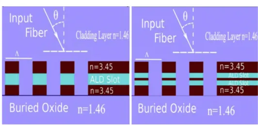
spectrum. Using simulations, the effect of the geometrical parameters and the ma-terial stack on the coupling spectrum was studied. The grating coupler schematics is shown in fig. 2.4. (Λ) represents the grating period. Atomic layer deposited slot layers are interposed by silicon layers. The fiber delivering the incident light is tilted at (θ) angle. The multiphysics simulations were organized as below:
1. The effect of the grating period on the coupling efficiency.
2. Slot size effect on the coupling. ( Slot size in case of horizontal slot waveguides is the thickness of the deposited slot layer.)
3. The effect of the slot material and refractive index on the coupling efficiency. 4. The effect of the bottom cladding thickness on the coupling efficiency.
2.2
Measurement Setup Features
In order to characterize the fabricated photonic chips, there is a need for a photonic probe-station. Electrical probe-stations are mature in the microelectronics industry. Research and industrial scale electrical probe-stations are commercially available. These probe-stations are facilitated by a number of electrical probes. The probes are connected to source/meter units that can apply or measure voltage and current. The probes can be used to characterize electron devices such as diodes, transistors or even electrical circuits. An important feature of these probe-stations is wafer scale measurements.
2.2. MEASUREMENT SETUP FEATURES 19
Wafer Scale Photonic Probestation
Inspired by the features mentioned above, a wafer-scale photonic probe-station was developed. The setup is presented in fig. 2.5. In order to characterize a photonic integrated circuit at least a pair of optical fibers are required. One optical fiber injects the input signal into a grating coupler while the other picks up the output signal from another grating coupler. A photonic probe-station can have the features as below [92]
1. Enabling wafer scale measurements. One of the benefits with grating couplers is wafer scale measurements. Unlike in the other couplers such as nano-tapers or butt couplers, the wafers do not require dicing.
2. Accommodate optical probes as well as electrical probes. This enables all-in-one electro-optical measurements.
3. Designed for grating couplers. Angled fibers almost touching the surface of the wafer. The position of the fibers need to be mechanically manipulated. 4. Tunable fiber angle. This enables the flexibility of the system for different
grating coupler designs.
5. Polarizers to change the polarity of the input signal. In addition to geometri-cal parameters, grating couplers are sensitive to the polarization of the input light. In case of slot waveguides the TM mode is only of interest.
6. Accurate XYZ positioners to efficiently deliver the guided beam onto the grating coupler surface.
The developed probe-station uses two fiber chucks to accurately point the fiber in a straight direction. The fiber chucks are held by steady fiber chuck holders fig. 2.6 (a) shows the fiber chuck and the fiber chuck holder. The fiber chuck holders are attached to a rotational stage. By means of this rotational stage the angle of the fiber can be tuned, as shown fig. 2.6 (b). The incident angle tuner has a precision of 6 Arc-second. Furthermore, the angle of the fiber can be measured by an accelerometer attached to the fiber chuck holder.
The rotation stages were mounted on XYZ piezo-motor positioners. This type of positioners were used for a maximal optical coupling. The best coupled optical signal is achieved if the beam spot is fitted inside the grating coupler surface. An accurate XY positioner can ensure that the spot is positioned at the most optimal location on grating coupler. The beam injected from the optical fiber is a Gaussian beam. This beam spatially diverges as it travels farther from the fiber tip. This makes the beam waist larger than that of the optical fiber core. In this work optical fibers with cores of 10.4 µm were used.
20
CHAPTER 2. THEORETICAL MODELS AND EXPERIMENTAL CONDITIONS
Figure 2.5: The probe-station with two optical fiber probes for light injection and pickup and two electrical probes.
Infra-Red Light Source
The laser beam is delivered from a solid state Agilent 81689A tunable laser. The wavelength can be tuned in the range of 1524 nm to 1576 nm. The highest laser power deliverable in the optical fiber is 5 dBm (0.003 W). The polarization of the input light is set by a polarizer. The picked up output signal from the chip is delivered to an IR detector. In order to measure the bandwidth of photodetectors a light modulator can be used to generate light pulses. This light modulator should be placed behind the polarizer and in front of the angled fiber stage.
2.2. MEASUREMENT SETUP FEATURES 21
Figure 2.6: (a) The fiber chuck and the fiber chuck holder. (b) Shows the the rotation station that holds the fiber chuck holder and is responsible for setting the angle of incidence.
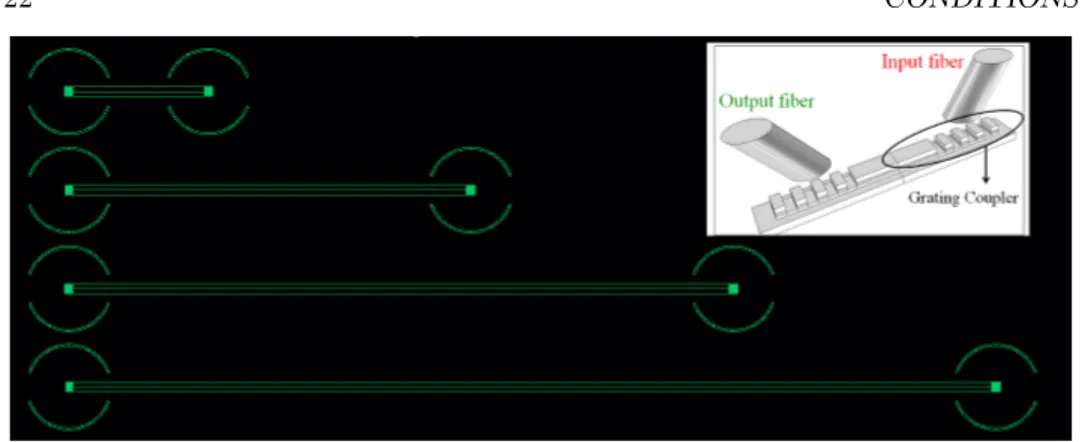
Characterization Methodology
The chips contained arrays of waveguide sets. Each element of the array contained a waveguide set with the same grating coupler period. The grating coupler period was incremented from 970 nm to 1060 nm with an increment of 10 nm. Each waveguide set had waveguides with incremented lengths. A sample waveguide set is depicted in 2.7. The transmission was measured for all of the waveguides in the set. The total loss in the optical links have two main components. The relation for the loss can be expressed as below if a logarithmic scale is assumed:
Lt(dB) = Lc (dB) + Lw (dB) (2.2)
Where Lt is the total loss in the optical link, Lc loss in the couplers (also
called the insertion lass), and Lwloss in the waveguide. optical loss was calculated
by subtracting the power (in dBm) transmitted in a pair of waveguides. This subtraction product was divided by the length difference to give the attenuation
22
CHAPTER 2. THEORETICAL MODELS AND EXPERIMENTAL CONDITIONS
Figure 2.7: The mask for the waveguide/grating characterization set. In every set, identical grating couplers were designed the waveguides had various lengths. This enabled loss measurements.
per unit length.
lw=
(P2− P1)
L2− L1
(dB
cm) (2.3)
In the equation above P represents the transmitted optical power and L the length of the waveguides. The measured transmission is a function of the coupling spectrum. The maximum transmission was used for 2.3. The total attenuation in the waveguide was found by multiplying the lw by the length of the waveguide.
This will give Lw in 2.2. Using the total loss Ltand the waveguide loss Lw in 2.2
the grating coupler insertion loss was calculated. This insertion loss corresponds to the insertion loss in a pair of grating couplers (input and output grating couplers). Since the calculations were done in the logarithmic scale the insertion loss in a single coupler is given by
lc =
Lc
2 (dB) (2.4)
Where lcis the insertion loss of a single grating coupler. This relation is based on
the reciprocity of the grating couplers [93]. In addition to the losses in the waveg-uides and the grating couplers, the coupling spectrum was measured for various grating periods.
Transmission Spectra Filtering Method
In order to give a more accurate measure of the coupler insertion loss, a filtering method was developed to suppress the coupling spectrum noise. This noise has interferometric patterns and is caused by resonance cavities. One of the major res-onance cavities is formed at the both ends of the waveguide and the back-reflections
2.2. MEASUREMENT SETUP FEATURES 23
Figure 2.8: The filtering method for the transmission spectrum. (a) The raw mea-sured transmission (b) the resonance features that need to be filtered (c) result of the band reject filter on the original spectrum. Reproduced from paper III in the thesis.
at the grating couplers. This filtering method is illustrated in fig. 2.8. In the mea-sured spectrum, two major type of fluctuations can be seen. In this method the intention is to filter a resonance pattern which corresponds to a rather small cavity. Fig. 2.8 (b) exclusively shows this fluctuation. In order to filter this pattern in the transmission spectrum a band reject filter was used. The result of this filter can be seen in Fig. 2.8 (c).
24
CHAPTER 2. THEORETICAL MODELS AND EXPERIMENTAL CONDITIONS
2.3
Thin Film Characterization Techniques
The high-k thin films were investigated during this work. This was done to optically characterize the slot layers and also evaluate the etching process. Spectroscopic el-lipsometry was extensively used to find the optical numbers associated with high-k layers and also etching of the high-k layers. For small features the mechanical pro-filer was used. This is due to a limit in the spot size of the ellipsometry equipment which is 200 by 200 µm.
Spectroscopic Ellipsometry
Ellipsometry is a contact free characterization technique. Dielectrics, semiconduc-tors, and thin metals can be studied using ellipsometry. Thickness, optical con-stants, roughness and other material properties can be measured. The physical principle of ellipsometry is to measure the change in the polarization of incident light as it interacts with the film(s) [94]. This change will appear by the reflections from different interfaces in the material stack, absorption in the films and also scattering effects. Spectroscopic ellipsometry uses a wavelength (in other words photon energy) spectrum of measurements to determine the optical constants and the thickness of the layers.
Each material is represented by their dispersion model. In order to measure the optical numbers, dispersion models were developed. An ellipsometric model includes the dispersion relations for each of the materials in the stack. The disper-sion relations are already developed and measured for well known and highly used materials in the industry. Crystalline silicon, poly-silicon, silicon dioxide and more are examples of these materials. In this work, the dispersion relation for the thin films, deposited by ALD, was developed. This is due to different film properties than reported in the literature.
The dispersion relation was developed by measuring several samples with de-posited high-k films. For each high-k material, samples were prepared with various film thicknesses. For each material a suitable dispersion model was used. For
Hf O2, Al2O3 and AlN a ’new amorphous’,’Cauchy absorbent’ and ’new
amor-phous’ models were used, respectively [95, 96]. The dispersion relation for each material is determined by the parameters in the dispersion models [92]. In order to find the right model parameters a set of fittings were done.
1. Silicon wafers with deposited high-k films were prepared. 2. The wafers were measured using spectral ellipsometry.
3. The model parameters were swept using initial guesses and the error (devia-tion from the measurement) was registered.
2.3. THIN FILM CHARACTERIZATION TECHNIQUES 25
In addition to this procedure, itterations were used to confirm the validity of the model. Assuming that the ALD has a constant deposition rate over time, samples with various thicknesses were prepared. Thickness of the high-k layer is determined by the number of deposition cycles. Therefore, it is expected that the film thickness is scaled with the number of cycles. The model was tested against different film thicknesses and the parameters were fine tuned through iterations. After this cycle the model that can predict a scaled thickness with the lowest error is accepted. Using this stable model, the optical numbers (n, k) were extracted from the ellipsometric dispersion relation.
Mechanical Profilometer
A mechanical profilometer is used to measure step height and roughnesses on a surface. It can also be used for film stress measurements. This technique is operated essentially in a contact mode. By horizontal scanning of a diamond stylus on the surface the variations on the surface are measured. An analog signal is generated by the change in the vertical position of the stylus. In case of small features this method was used to measure the etch depth in high-k layers to find the etch rates. The profilometer was also used to measured the step height of the grown germanium mesas and the etched germanium.
Chapter 3
High-k Slot Grating Couplers
This chapter studies the slot grating coupler design and the theoretical performance of the couplers. Single slot fully etched, double slot fully etched and single slot partially etched coupler designs will be investigated. The effect of the slot layer thickness and material will be also explained.
3.1
Fully Etched Grating Coupler Design
The grating couplers for crystalline silicon waveguides are partially etched. The periodic grating structure is patterned using a different mask than the waveguide and the etching is done triggering an accurate etch depth. The grating coupler operation is sensitive to this etch depth and angle of incidence [97, 98]. This can be avoided by a fully etched design. However, the refractive index contrast between silicon and the cladding material (SiO2) is high. A fully etched grating coupler for
crystalline silicon will suffer from high back-reflections [99]. Due to these reflections the efficiency will be very poor.
On the other hand, slot waveguides have a much lower effective refractive index than an all-silicon waveguide. This is due to a high confinement of the guided mode in the low refractive index slot region. Taking advantage of this property of the slot waveguides, it was possible to make fully etched slot grating couplers. A fully etched structure features:
1. A Single mask process. The waveguides and the grating couplers are fabri-cated through the same mask.
2. A More reproducible device manufacturing process. The grating coupler yield is affected by the variation in the etch depth. This is solved in a fully etched design.
The partially etched grating couplers for the SOI photonics should not be mis-taken with the grating couplers introduced in 3.2. The partially etched slot grating
28 CHAPTER 3. HIGH-K SLOT GRATING COUPLERS
couplers in 3.2 use a single mask step like their fully etched counterparts. This design can be used regardless of the number of the slot layers in the waveguides. In this work single and double slot high-k slot couplers will be presented.
Fabrication Process Considerations
The grating couplers were designed to be compatible with the in-house processing equipment. One of the limitations in the fabrication process was the lithography resolution. In order to pattern the waveguides and the grating couplers an i-line stepper was used. The grating couplers have a filling factor of 50 %. This means that the smallest resolvable grating period is 960 nm. Because of a lowered effective refractive index in the slot waveguides the grating coupler period is not limited by this resolution.
The device structure was designed for an etching endpoint detection system. The etch endpoint detection algorithm in a dry etching equipment is responsible for stopping the etch process [100]. This mechanism is triggered when the etching of the material is finished and another material layer is reached. In the case of the fully etched grating couplers, the last etching step is the bottom silicon etch. This etch step will be stopped by the endpoint detection algorithm at the bottom SiO2
cladding layer.
Theoretical Grating Coupler Performance
Grating couplers with Al2O3, Hf O2, and AlN high-k slot layers were simulated.
The bottom SiO2 layer causes strong reflections at the waveguide and substrate
interfaces. These reflections make interference patterns at the grating coupler. Due to this interference pattern, the coupling efficiency can be enhanced or degraded. By using an infinite SiO2 bottom layer in the simulations an average coupling
efficiency was calculated.
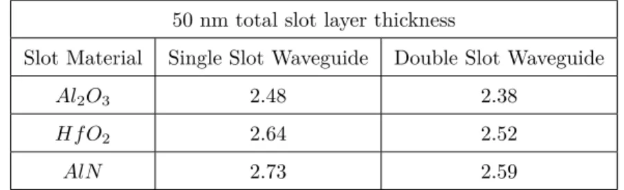
The slot waveguide was formed by two 220 nm silicon layers interposing a 50 nm high-k ALD layer. The high-k layer in this simulation was Al2O3. For this slot
waveguide The grating coupler a 990 nm grating period was required to achieve a peak efficiency at 1.55 µm. Fig. 3.1(a) shows the peak efficiency of 24 % and 80 nm 3dB-bandwidth was calculated. To compare the performance and efficiency tolerance to the variations, a partially etched structure was also simulated. An efficiency peak at 1.55 µm was achieved with a grating period of 935 nm. The coupling efficiency was 30 % and the 3 dB bandwidth was 75 nm. Since an infinite silicon oxide layer was used in the simulations the efficiency has an average value. In all grating coupler designs the bottom and top cladding layer are highly reflective [101].
The simulations showed that a partially etched grating coupler with less etch depth have higher efficiencies. Shallower etch depth creates less perturbations in the waveguide. Less perturbation in the waveguide will have a weaker effect on the effective index. A lower refractive index contrast will cause less back-reflections
3.2. NOVEL PARTIALLY ETCHED COUPLER DESIGN 29
Figure 3.1: (a)Performance of the fully etched grating couplers and comparison with partially etched grating couplers. (b)Sensitivity of partially etched grating couplers to the etch depth. Reproduced from the paper I in the thesis [102].
from the grating coupler to the waveguide and increase the coupling efficiency. However, the calculated grating periods for shallower etch depth required a smaller grating period. The partially etched grating coupler simulated here as an example, had a grating period of 935 nm, which was out of the lithography resolution limits. The partially etched couplers show a higher efficiency. Despite this higher ef-ficiency, it is worthwhile to study the sensitivity of the grating couplers to the variations in etch-depth. Fig. 3.1(b) shows the performed simulations with varied etch depths. The simulations showed that a 10 nm over-etching of the grating structure degrades efficiency at 1.55 µm by 3 percent. This degradation was even more severe with a 20 nm over-etching. The coupling efficiency was lowered to 23 % at 1.55 µm. In 3.2 a partially etched grating coupler is discussed. This solution solves the variation tolerance problem of the partially etched couplers. In addition, a more suitable grating period was achieved to fit the lithography resolution. This was done by using a thicker slot layer. The effect of the slot thickness on the grating period is discussed in 3.4.
3.2
Novel Partially Etched Coupler Design
The schematics of this grating coupler is shown in Fig. 3.2. One of the main features of this slot coupler is that the slot layer in not at the center of the waveguide. Moving the slot layer towards the bottom silicon layer will result in a grating period which is suitable for the lithography resolution.The fabrication process has the following details
30 CHAPTER 3. HIGH-K SLOT GRATING COUPLERS
Figure 3.2: Schematics of the partially etched slot waveguide design.
2. It is straightforward to achieve a precise etch depth. The high-k ALD slot layer is a good etch stop and the top silicon etching is stopped by endpoint detection.
This design is specially useful for embedding of 2D materials in the slot waveg-uide [103]. In chapter 5 embedded graphene photodetectors are introduced. Due to its 2D nature, graphene layers can be harmed during etching steps. In order to embed the graphene inside the waveguide it needs to be buried in a protective film. The high-k slot layer can protect the graphene from unwanted harm during the rest of the fabrication process. The partially etched grating coupler and waveguide is a suitable design for this application.
3.3
Double Slot Vs. Single Slot Waveguides
Increasing the number of slots in a slot waveguide can increase the slot effect [104]. A double slot waveguide will have a higher mode density in the slot region than a single slot waveguide. In case of embedding an optically active material in the slot region a double slot structure is favorable. The interaction between the optical mode and the active material is higher in a double slot structure [105]. Using this effect, active photonic devices with smaller footprints can be manufactured.