THESIS
ADVANCED RESEARCH DEPOSITION SYSTEM (ARDS) FOR PROCESSING CdTe SOLAR CELLS
Submitted by Keegan Corey Barricklow Department of Mechanical Engineering
In partial fulfillment of the requirements For the Degree of Master of Science
Colorado State University Fort Collins, Colorado
Summer 2014
Master’s Committee:
Advisor: Walajabad Sampath James Sites
Copyright by Keegan Corey Barricklow 2014 All Rights Reserved
ii
ABSTRACTADVANCED RESEARCH DEPOSITION SYSTEM (ARDS) FOR PROCESSING CdTe SOLAR CELLS
CdTe solar cells have been commercialized at the Gigawatt/year level. The development of volume manufacturing processes for next generation CdTe photovoltaics (PV) with higher efficiencies requires research systems with flexibility, scalability, repeatability and automation. The Advanced Research Deposition Systems (ARDS) developed by the Materials Engineering Laboratory (MEL) provides such a platform for the investigation of materials and manufacturing processes necessary to produce the next generation of CdTe PV.
Limited by previous research systems, the ARDS was developed to provide process and hardware flexibility, accommodating advanced processing techniques, and capable of producing device quality films. The ARDS is a unique, in-line process tool with nine processing stations. The system was designed, built and assembled at the Materials Engineering Laboratory. Final assembly, startup, characterization and process development are the focus of this research. Many technical challenges encountered during the startup of the ARDS were addressed in this research. In this study, several hardware modifications needed for the reliable operation of the ARDS were designed, constructed and successfully incorporated into the ARDS. The effect of process condition on film properties for each process step was quantified. Process development to achieve 12% efficient baseline solar cell required investigation of discrete processing steps, troubleshooting process variation, and developing performance correlations. Subsequent to this research, many advances have been demonstrated with the ARDS. The ARDS consistently produces devices of 12% ±.5% by the process of record (POR). The champion cell produced to date utilizing the ARDS has an efficiency of 16.2% on low cost commercial sodalime glass and utilizes advanced films.
The ARDS has enabled investigation of advanced concepts for processing CdTe devices including, Plasma Cleaning, Plasma Enhanced Closed Space Sublimation (PECSS), Electron Reflector (ER) using Cd1-xMgxTe (CMT) structure and alternative device structures. The ARDS has been instrumental in the collaborative research with many institutions.
iii
ACKNOWLEDGEMENTS
First and foremost, I want to acknowledge the love and support of my wife, Jessica. Without her patience and gentle persistence to encourage my accomplishment in this endeavor, my passion for the outdoors may have forever distracted me. To my family, for always reminding me that I “know it all”, and while certainly far from the truth, their confidence gave me ambition to prove them right. To my friends, for always understanding that play must wait until the work is done. You gave me motivation to work harder, to earn the rewards of completion.
I want to thank Jim Sites for your contribution my knowledge of PV physics and device characterization. The resources that you have established through the PV Characterization Lab, both personnel and equipment, have been instrumental to advancing the research in this study. The body of literature reflecting your contribution to the field is respectable and highly valuable.
For his personal commitment to my success, for always having great advice, and for supporting the opportunity to pursue this degree, I cannot thank Anders Olsson enough. You have demonstrated excellence in leadership that I hope to eventually achieve.
For the opportunity to make a contribution to the PV field, I give many thanks to Dr. Sampath, Kurt Barth and Al Enzenroth. The Materials Engineering Lab and Abound Solar have been most profound in defining who I am as a professional. The members of the MEL and Abound Solar demonstrated great confidence in my abilities and reciprocated great knowledge and guidance, without their support this research would not have been possible.
The success of the ARDS has been achieved only by the hard work of many. The members of the MEL, Paul Kobyakov, Jason Kephart, Drew Swanson, and Kevin Walters supported diverse activities to successfully bring the ARDS into the current state of operation. The R&D team at Abound Solar including Nathan Schuh, Alan Davies, Nicole Landou, Richard Hafer, Nirav Vora, Kishore Kamath and Anders Olsson .provided critical support, experience, interpretation and guidance necessary to the success of this research. Neil Scofield and Steven Barnes were vital to the rapid production of small area devices (SAD) and Lei Chen for supporting measurement equipment and characterization requests. I thank Bill Yates for support and training on the operation of microscopy techniques used for this research. The members of the PV characterization lab, specifically Russel Geisthardt, Valerie Jacobson, Tyler McGoffin, John Raguse, and Katherine Zaunbrecher have provided pertinent device characterization and analytical interpretation. Pat McCurdy and Den Heyes of the CSU Central Instrumentation Facility provided training of advanced material characterization techniques.
iv
I thank all of my peers for the opportunity to grow with you, my predecessors for the opportunity to learn from you and my colleagues at Abound for the opportunity to change the world. To all those who have supported the MEL and PV Characterization lab, thank you, thank you, thank you, for your contribution to finding a better solution.
This work was completed with funding from the NSF I/UCRC – Next Generation Photovoltaics Center, NSF-AIR Program, and Abound Solar.
v
TABLE OF CONTENTS
ABSTRACT ...II ACKNOWLEDGEMENTS ... III
CHAPTER 1: INTRODUCTION AND MOTIVATION ... 1
1.1WHY RENEWABLE ENERGY? ... 1
1.2FUNDAMENTALS OF A SOLAR CELL ... 4
1.3CDS/CDTE SOLAR CELL ... 7
1.4STATE OF THE TECHNOLOGY/STRUCTURE ... 8
1.5ROADMAP OF RESEARCH ... 9
1.6THE ADVANCED RESEARCH DEPOSITION SYSTEM ... 11
1.7THE NEED FOR AUTOMATION OF EXPERIMENTS ... 12
1.8STATEMENT OF WORK ... 12
1.9SUPPORTING MEMBERS ... 12
CHAPTER 2: EXPERIMENTAL DETAILS ... 13
2.1CELL FABRICATION ... 13
2.2FILM AND DEVICE CHARACTERIZATION ... 14
2.2.1 Current-Voltage (J-V) ... 14
CHAPTER 3: ADVANCED RESEARCH DEPOSITION SYSTEM ... 16
3.1BASIC SCHEMATIC AND VACUUM PARAMETERS ... 16
3.2PROCESS OUTLINE ... 17
3.3SUBSTRATE PREPARATION ... 17
3.4PLASMA CLEANING ... 18
3.5SUBSTRATE TRANSFER AND MANIPULATION ... 18
3.6HEATED POCKET DEPOSITION SOURCE DESIGN ... 19
3.7HEATED SHUTTER ... 23
vi
3.9PROCESS CONTROL ... 24
3.10INTEGRATION AND STARTUP ... 24
CHAPTER 4: PROCESS DEVELOPMENT AND DEVICE RESULTS ... 27
4.1METHODOLOGY ... 27
4.2CLOSED SPACE SUBLIMATION BASICS ... 28
4.3PROCESS SPACE ... 30 4.4SUBSTRATE HEATING ... 30 4.5CDSOPTIMIZATION ... 31 4.6CDTE OPTIMIZATION ... 36 4.7CDCL2OPTIMIZATION ... 41 4.8CUCL PROCESS OPTIMIZATION ... 49
4.9DEVICE OPTIMIZATION AND PROCESS OF RECORD ... 53
4.10ADDITIONAL STUDIES ... 57
4.10.1 Intermediate CdCl2 treatment of CdS prior to CdTe (CdS/CdCl2/CdTe) ... 57
4.10.2 Precision Glass and Optics substrate with Indium Tin Oxide (ITO) TCO ... 61
4.10.3 EL, PL, DLIT Studies ... 64
CHAPTER 5: CONCLUSIONS ... 66 5.1PROGRESS ... 66 5.2CHALLENGES ADDRESSED ... 68 5.3PERSPECTIVE ... 68 5.4FUTURE WORK ... 68 REFERENCES ... 69 APPENDIX ... 74
A1ADDITIONAL CHARACTERIZATION TECHNIQUES ... 74
A1.1 Capacitance-Voltage ... 74
vii
A1.3 Ultra Violet-visible spectroscopy (UV-Vis) ... 74
A1.4 Atomic Force Microscopy (AFM) ... 74
A1.5 Profilometry ... 75
A1.6 Scanning Electron Microscope ... 75
A1.7 X-ray Photoelectron Spectroscopy (XPS) ... 75
A1.8 X-ray Diffraction (XRD)... 75
A1.9 X-ray Fluorescence (XRF) ... 75
A1.10 Photoluminescence (PL) ... 75
A1.11 Electroluminescence (EL) ... 76
1
CHAPTER 1: INTRODUCTION AND MOTIVATION
1.1 Why Renewable Energy?
Directly converting sunlight to electricity by means of the photovoltaic effect is the most elegant form of energy conversion. As the global community recognizes the limited resources and detrimental effects of conventional fossil energy, additional efforts will be made to utilize renewables. Trends indicate global energy demands will increase 56%, with fossil fuels accounting for 80% of energy production, and increased CO2 emissions of 46% by 2040 [1]. According to the US Energy Information Administration (EIA), future US electricity generation by non-hydropower renewables will nearly double by 2040 as indicated in Figure 1-1 [2].
Solar energy presents a viable alternative source of energy to meet the global energy and environmental demands. An increase in non-hydro power renewables is expected as new technologies demonstrate increased efficiency, and reduced manufacturing costs. The depletion of easily accessible fossil fuel resources will drive energy costs upward, and stimulate popular interest in sustainable energy technologies. As we move towards a globally modernized and expanding population, supplying the global energy demands will continue to be a significant challenge. Figure 1-2 demonstrates the exponential energy consumption, even as population growth starts to stabilize. The need to balance current energy practices with renewable resources is critical for achieving a sustainable energy future.
2
Figure 1-2: World population and energy demand growth. [3]
A sustainable energy portfolio would include a blend of renewable technologies such as wind, hydro, bio and solar in addition to limited fossil fuel and nuclear sources. Annual global installations of new PV expanded between significantly from 2000-2011, as presented in Figure 1-3. The EIA predicts electricity generation from renewables to nearly double by 2040, with an increasing renewable generating capacity resulting from solar as seen in Figure 1-4 respectively. While it is accepted that most renewable technologies have energy production limitations due to variation in environmental conditions, the ability to offset peak demands is significant.
Solar photovoltaic technologies are well suited to be installed at point of use in residential and commercial space, and are becoming common among dual purpose shade structures and commercial rooftop installations. Photovoltaics are ideal for these applications due to the simplicity, versatility, reliability, and low environmental impact of installations. Large utility installations are becoming more popular in the arid southwest where the land is not suitable for agriculture, but has excellent solar resources [4]. With the development of the smart grid and advancements in the electrical distribution infrastructure, renewable energy integration will become increasingly manageable [5] In addition to the improvements in grid transmission; integration of renewable technologies into construction has opened new venues previously too valuable for low density energy production [6]. Capitalizing on the available solar resources would enable practical diversification of the global energy portfolio.
3
Figure 1-3: Global annual new installed capacity of solar PV and wind, 2000-2011 [7]
Figure 1-4: Predicted renewable electricity generating capacity by energy source. [2]
With reductions in manufacturing costs, improvements to conversion efficiency, and public acceptance, photovoltaics will become an important source of economical premium-quality power. Trends tell us that module and balance of systems (BOS) costs will continue to diminish with increased capacity and improved technologies. The Department of Energy (DOE) launched the SunShot Initiative to stimulate the revitalization of photovoltaics research by the private sector after continued decreases in the market share of solar manufacturing. The SunShot program has a target cost of electricity from PV systems of $.06 per kilowatt-hour (kWh) by 2020; effectively achieving grid parity, and making solar a sustainable industry without subsidies. While the program is just a few
4
years old, it has already accomplished a 60% reduction in the cost of utility-scale systems [8]. Market trends demonstrate the significant reduction in the cost per watt ($/watt) of module pricing as seen in Figure 1-5, which directly affects the residential and utility system costs.
Figure 1-5: Price forecasts of solar system; forecast with post 2008 curve. Figure reproduced from [7] 1.2 Fundamentals of a Solar Cell
When one or more semiconductor materials are joined to form a p-n diode, a solar cell is created. A solar cell converts light photons to electrical current through the photovoltaic effect. Using solar photovoltaics to transforming just a fraction of the solar energy reaching the earth would have a significant impact on the energy picture.
Sunlight is a portion of the electromagnetic radiation emitting from the sun. We define sunlight as a spectrum of discrete units of energy called photons, whose energy is based on wavelength. Light reaching the earth has a spectral distribution that affects the potential efficiency of a solar cell. The spectrum as measured at the edge of the earth’s atmosphere is considered the solar constant of air mass zero (AM0). As the radiation passes though earth’s atmosphere, it interacts with gases and aerosols that cause significant losses due to absorption, reflection and scattering. The spectrum incident on a surface at sea level with a zenith angle of 37deg, is denoted air mas 1.5global (AM1.5g), and has a normalized intensity of 1,000 W/m2 [9]. This distribution accounts for both diffuse and direct irradiance, as solar cells are effective at converting both. The AM1.5 spectral distribution is recognized as the standard for terrestrial characterization.
5
Figure 1-6: The AM1.5global solar radiation spectrum. [9] [10]
Only photons with energy higher than the band gap of the semiconductor are absorbed and contribute to the generation of electrical energy. The band gap of a direct-gap semiconductor is the difference in energy between the top of the valence band and the bottom of the conduction band, defining the energy necessary to generate an electron-hole pair. Figure 1-7 represents the band diagram of a basic single junction solar cell under illumination. The Shockley-Queisser model, predicts the efficiency limits for p-n junction solar cells using the Eg of the absorber layer. Graphically represented in Figure 1-8, one can see the ideal theoretical conversion efficiency of CdTe solar devices.
6
Figure 1-8: Shockley-Queisser efficiency limit of single junction solar cells. [12] [13]
A p-n heterojunction is established when different p-type and n-type semiconductors are joined. As demonstrated in Figure 1-9, carriers immediately diffuse across the junction resulting ionized atoms and establishing neutral regions of fixed charge. This space charge region becomes depleted of both electrons and holes, producing a built in field that acts as a barrier to the further drift of majority carriers and presents a low resistance path to minority carriers. With illumination, the built in field causes charge separation, driving electrons to the n-side and holes to the p-side inducing photo-generated current and performing work when attached to an external load.
7
Hetero-junctions are limited by the formation of interface states which work to trap charges at the junction, reducing the built in voltage. A quantifiable performance gap exists between lab and ideal efficiencies, related to open circuit voltage (Voc), Fill-Factor (FF), and short circuit current (Jsc). Performance losses due to these parameters are well explained by Sites and others [15] [16]. Developing better correlations between process, performance and structure should allow improvements to all parameters. The performance gap between lab and commercial efficiencies are expected to reduce as advanced manufacturing techniques are achieved to improve window layers, uniformity and cell interconnections.
1.3 CdS/CdTe Solar cell
Solar cells are formed through the assembly of n-type and p-type semiconductor layers. Thin film structures are formed directly on substrates consisting of polymers, glass, metal or ceramics. Solar devices may be produced in either a superstrate or substrate configuration depending on process and application. A superstrate configuration is most common for fabrication ease and encapsulation quality. In this configuration the incident light first passes through the substrate before being absorbed in the photojunction. This structure requires the use of a highly transparent substrate, and transparent conductive oxide layer (TCO).
Terrestrial solar applications have an optimal bandgap of ~1.5eV [17] [13]. Selection of a material system for large scale applications is based on potential device efficiency and manufacturing costs resulting the metric of $/kWh. The use of CdTe is attractive as it is a direct gap semiconductor with a bandgap of ~1.45eV, and high absorption coefficient. These qualities result high conversion efficiencies of wavelengths up to ~810nm with absorber layers of ~2µm thickness. The typical heterojunction CdTe device utilizes an n-type CdS window layer with a band gap of ~2.42eV. This wide bandgap allows transmission of wavelengths greater than ~510nm when thin layers are used.
Various techniques for manufacture of CdS/CdTe thin film solar cells are possible, including chemical bath deposition (CBD), closed space sublimation (CSS), physical vapor deposition (PVD) and vapor transport deposition (VTD). Both CdS and CdTe are well suited to closed space sublimation (CSS). Films grown by CSS have many advantages over low temperature processes; producing excellent microstructure, and device performance when treated with a high temperature CdCl2 process. High volume manufacturing benefits of CSS include high deposition rates, large area uniformity, and excellent material utilization. Record device efficiencies have been
8
produced by CSS and VTD techniques. The CdTe solar cell described herein is produced using a novel heated pocket deposition (HPD), a variation of closed space sublimation (CSS).
1.4 State of the Technology/Structure
Significant advancements in performance and cost reduction have been accomplished in thin film solar spurring increased installations, especially at the utility scale. First Solar is currently the leading global provider of solar systems utilizing CdTe thin film with more than 8GW installed worldwide. Reported by NREL, the historical research-cell efficiency records are presented in Figure 1-10. Significant progress has been made in field of thin film CdTe technologies since 2011. In February 2014, First Solar announced a record setting research cell of 20.4%, besting its previous of 19.6%. This accomplishment matches the multicrystalline Si research cell efficiency, which are nearing ultimate entitlements. In 2009, First Solar became the first solar panel manufacturing company to lower its manufacturing cost to $1 per watt. This Arizona based Auga Caliente solar project demonstrates electricity production at $0.06/kWh, near grid parity. It is one of the largest operational PV power plants in the world (Figure 1-11), with a generating capacity of 290MWp of alternating current [18].
9
Figure 1-11: Agua Caliente solar farm, First Solar [20] 1.5 Roadmap of Research
There are many approaches currently under investigation for improving the efficiency of CdTe solar devices. The focus at the Colorado State University Materials Engineering Laboratory (MEL) is that of volume manufacturing techniques. Target objectives are improvements to the window layer transmission, reducing bulk recombination, improving back contact quality and the development of the electron reflector.
Working closely with the Colorado State University Electric Propulsion and Plasma Engineering Lab (CEPPE), incorporation of plasma enhancing techniques for the preparation and deposition of films are being investigated. Exposure of the TCO to low energy plasma just prior to deposition has shown to reduce shunting defects and improve material density [21] [22]. Plasma Enhanced Close Space Sublimation (PECSS) has been demonstrated for improving species incorporation during deposition and benefits film uniformity. The novel hollow cathode concept can be readily incorporated in existing systems and has been tested in large format and volume production environments. Both of these techniques enable thinning of the CdS window layer, increasing blue spectrum response and current densities [23]. Broadening of the CdS bandgap can reduce absorption loses in the window layer. In addition to PECSS, sputtering CdS in the presence of Oxygen to form CdS:O has been demonstrated [24].
10
Figure 1-12: HPD Co-sublimation source used for CMT (B) with PECSS (A).
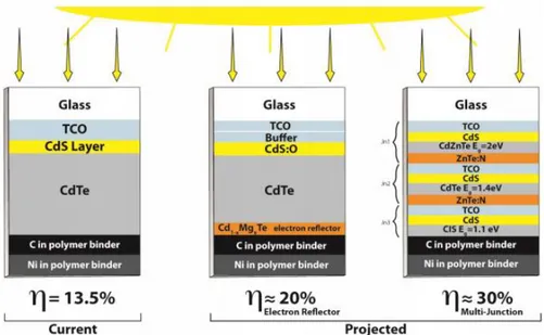
Another area of research is in creating a layer of Cd1-xMgxTe (CMT) at the back of the absorber, that would lead to the formation of an electron reflector at the back of the current structure [25] [26]. Multiple techniques for depositing the absorber layer, including the HPD co-sublimation source (Figure 1-12) developed at the MEL. Preliminary results demonstrate feasibility of creating a higher band gap material by means of co-sublimation, and are accordingly a focused effort. The roadmap of the Materials Engineering Laboratory and National Science Foundation Next Generation Photovoltaics Industry/University Center for Research Collaboration (I/UCRC) to pursue higher efficiency through incorporation of sputtered CdS:O and multiple-junction cells is presented in Figure 1-13. The devices in this study have the structure marked as current.
11
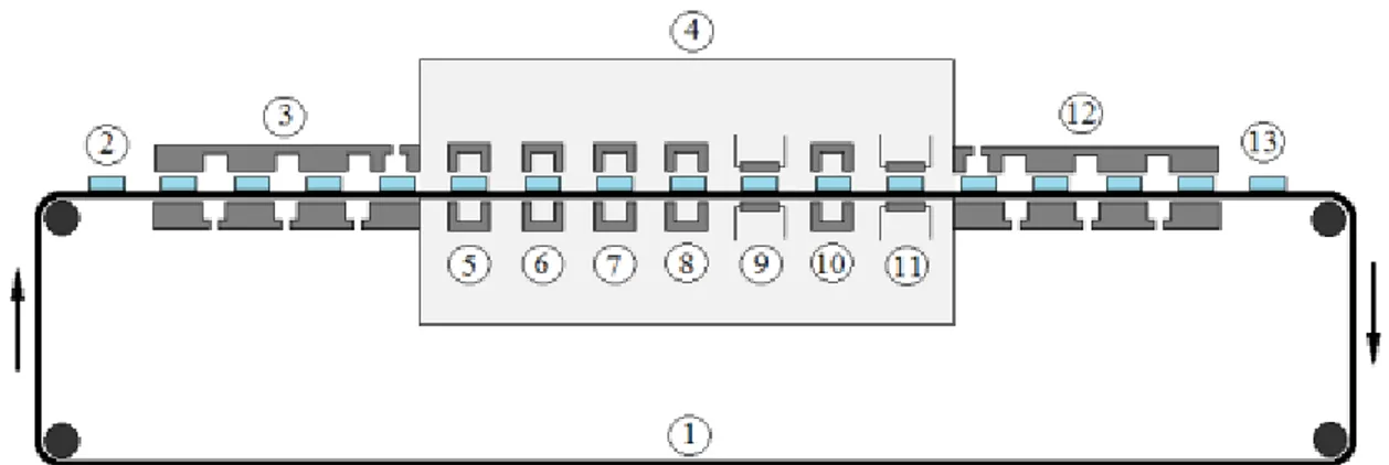
1.6 The Advanced Research Deposition SystemThe original R&D system developed at the MEL was a continuous, in-line process, transporting samples from Air to Vacuum to Air (AVA) on a continuous belt conveyor represented in Figure 1-14 [27]. The AVA system was conceived to demonstrate volume manufacturing of the thin film solar process, and eventually achieved success with the startup of Abound Solar (Formerly known as AVA Solar). The HPD process combined with a conveyor transport is suitable for production, but is limiting in all aspects of research. The AVA system utilized a multistage molecular seal instead of common load lock configurations. This necessitated specific substrate tolerances to maintain process pressure, limiting the ability to test alternative substrate geometries. There was no ability to generate partial or intermediate films while simultaneously producing full devices. As the samples were continuously exposed to the high temperature sources, motion had to be maintained. This meant that a large number of transient samples were produced between target set-points, and the potential for process drift to occur was common.
Figure 1-14: Diagram of AVA system developed at the MEL. (1) continuous conveyor belt (2) base glass substrate (3) AVA seal (4) vacuum chamber (5) substrate heating (6)CdS deposition (7)CdTe deposition (8) CdCl2 deposition (9) CdCl2 annealing and stripping (10) back contact formation (11) back contact annealing (12)AVA molecular seal
(13) completed device
To achieve experimental flexibility, and maintaining a concept capable of volume manufacturing, an in-line research tool was necessary. Considering current and future process limitations, a linear tool configuration utilizing the well-established HPD technique was developed. The ARDS design enabled hardware and process flexibility, with the potential for future additions. The linear layout was selected for ease of sample transport and necessitated by an existing boundary limitation. The hardware was designed to be modular, providing a spatial envelope for which prototype hardware could be tested, including alternative deposition techniques. The single sample transport mechanism allows variation of substrate type, process sequence, dwell times, and the ability to generate intermediate
12
films for characterization. The ARDS provides a highly versatile platform for development of next generation solar cells, and key features will be presented in Chapter 3, process characterization and results discussed in Chapter 4. 1.7 The need for Automation of Experiments
Experimental efficiency minimizes time, resources and waste. Carefully controlling the manufacturing process is necessary to produce meaningful and repeatable results. Automation of the ARDS is accomplished by the integration of process controls through a custom Labview interface. Operators’ are able to define process recipes, load a substrate, and let the machine do the rest, eliminating user variation. All valve actuation for transfer, pumping and purging is automated, minimizing disruptions to the process environment and potential damage to the equipment. Compared to the previous AVA system, the ARDS executes experimentation with significantly fewer transient samples.
1.8 Statement of work
The purpose of this research is the integration, startup and process development on the ARDS. In addition to the startup and process development, secondary requirements included the development of techniques for glass preparation, chemical processing and establishing chemical containment and safe practices to limit and monitor Cadmium migration and exposure. Considerable effort was put into the development of procedures and documentation necessary for the maintenance and operation of the ARDS, including training of students.
1.9 Supporting members
The Materials Engineering Laboratory is supported by students and faculty with diverse skills, and a passion for PV technology. Undergraduate, graduate and Ph.D. level students’ research advanced concepts for improving manufacturing technologies and characterization. My peers, Paul Kobyakov, Jason Kephart, Drew Swanson, and Kevin Walters brought valuable skills to the MEL team. Paul’s characterization and interpretive capacity was highly beneficial to process optimization. The focus on improved window layers by Jason and Drew, supported incremental optimization of the device structure. Jason’s expertise with Labview supported automation development. Thermal modeling by Kevin provided insight to hardware improvements, and mechanical optimization. Detailed characterization of devices by Russel Geisthardt, John Raguse, Tyler McGoffin, Katherine Zaunbrecher and Jim Sites of the PV Characterization lab enhanced process to performance correlations. Their assistance was highly valuable and necessary to the success of the ARDS.
13
CHAPTER 2: EXPERIMENTAL DETAILS
2.1 Cell Fabrication
Baseline cells are fabricated on low cost commercially available soda lime float glass with a pyrolytically deposited transparent conductive oxide (TCO) layer. The TCO is typically a fluorine-doped SnO2 layer, which serves as the front electrical contact. The ARDS is designed to utilize 3.6” x 3.1” substrates, or a high temperature carrier to facilitate smaller samples. A high temperature CSS process is used for the subsequent deposition of n-type CdS, p-type CdTe, CdCl2 activation and back contact doping, resulting the device structure presented in Figure 2-1.
Figure 2-1: Superstrate structure of CdTe solar cells produced with ARDS.
Finished photodiodes are removed from vacuum and rinsed in deionized (DI) water to remove excess CdCl2 residual. Samples are inspected and divided according to research needs, raw films are immediately desiccated or stored in an inert environment glovebox, and films to be used for solar cells are prepared with back electrode. The back contact is formed by spray application of a thin layer (~2µm) of colloidal carbon, followed by thicker layer (~100µm) of nickel particle in acrylic binder onto the exposed CdTe surface [28]. Small area devices (SAD) are formed by careful masking and abrasive blasting to define active cell regions of approximately 0.7cm2 as represented in Figure 2-2.
14
2.2 Film and Device CharacterizationAll solar cells and partial films studied in this research were generated with the ARDS. Many techniques are used to fully assess the material and the electrical characteristics of solar cells. These techniques are common to thin film characterization and are well defined in literature. The techniques used for the electrical characterization of devices are Current density-Voltage (J-V), Capacitance-Voltage (C-V), and Quantum Efficiency (QE). Techniques used to investigate discrete film properties are UltraVioliet- Visible spectroscopy (UV-Vis), Profilometry, Atomic Force Microscopy (AFM), Scanning Electron Microscopy (SEM), X-ray Photoelectron Spectroscopy (XPS), X-ray Diffraction (XRD), X-ray Fluorescence (XRF). Advanced device and film characterization by Photo-Luminescence (PL), Electro-Luminescence (EL) and Time Resolved Photo-Luminescence (TRPL) are used to evaluate defect state and minority carrier lifetime. This suite of techniques is used to correlate process conditions to film and device performance. The results presented are not exhaustive, and specific to the discoveries associated with the ARDS.
2.2.1 Current-Voltage (J-V)
Measuring current density as a function of applied voltage (J-V), under controlled illumination and temperature provides whole cell performance, and key parameters relating to device quality and conversion efficiency. It is useful to visualize the solar cell with an equivalent electrical circuit as Figure 2-3. An IV measurement is performed by monitoring the device response to an applied voltage, from 0 volts (short circuit) to the open circuit voltage, with constant AM1.5g illumination. The current measured at zero voltage is the short circuit current Isc (mA) and is often discussed in terms of short circuit current density (Jsc) expressed as (mA/cm2) The open circuit voltage (Voc) is measured at zero current. Figure 2-4 represents a common IV curve, and identifies these parameters. From the IV curve a power curve can be generated, identifying the maximum power voltage (Vmp), maximum power current density (Jmp), and maximum power point (MPP). The power lost due to series and shunt resistance is represented with fill factor (FF). Fill factor is a ratio of MPP to the product of Vocand Jsc. Parasitic losses from shunt (Rsh)and series (Rs)resistances reduce the FF. Device efficiency (η) is calculated as a ratio of produced power to the power input. Test methods and apparatus are well defined by Davies [29].
15
Figure 2-3: Equivalent circuit of a solar cell [11]
16
CHAPTER 3: ADVANCED RESEARCH DEPOSITION SYSTEM
3.1 Basic Schematic and Vacuum ParametersThe ARDS is an inline, single vacuum research tool (Figure 3-1) with an isolating load lock for sample exchange. There are a total of 9 modular stations to accommodate cell fabrication as depicted in Figure 3-2. A simple racking system allows integration of alternative source technologies, including PECSS and Co-Sublimation.. Vacuum is accomplished by a combination rotary vane and diffusion pumps, to achieve a process of record (POR) deposition pressure of 40mT. Background gas can be premixed or custom blended to satisfy research interests. Typically a high purity gas blend of 2%O2 in N2 is used for all baseline studies, but can be tailored to specific composition using a gas manifold and MFCs (Figure 3-3). A Residual Gas Analyzer (RGA) is utilized for monitoring the residual composition prior to and during deposition.
Figure 3-1: ARDS System prior to implementation of control environments.
17
Figure 3-3: ARDS expansion ports, pyrometers and gas delivery. 3.2 Process Outline
The ARDS is based on the process developed in the AVA system. The source hardware is arranged sequentially and coincidentally by the thermal profile of the process. After performing the plasma treatment of the TCO, the substrate is rapidly heated to ~500C. Subsequent CSS depositions of CdS and CdTe occur, followed by a CdCl2 activation sequence. After cooling of the film, a low temperature CuCl back contact is applied and annealed. All steps are performed in a common environment, without breaking vacuum. The ARDS is easily modified to accomplish unique research tasks while allowing large combinations of process conditions.
3.3 Substrate Preparation
Substrates received from the manufacturer are packed with a paper interleaving. Samples are inspected for edge damage or defects in the field of deposition. They are then sorted by TCO orientation and inserted into a stainless wash rack with perimeter supports only. Immediately prior use, the substrates are suspended in an ultrasonic bath with a heated solution of de-ionized (DI) water and surfactant for one hour. A thorough DI water rinse is performed to remove detergent from the substrates, ensuring no residue is allowed to dry. The samples are then transferred to a second ultrasonic tank for a final DI water agitation for an additional 30minutes. The samples are quickly moved to a static isopropyl alcohol bath for 20minutes. Upon expiration of this time, samples are removed, allowing the IPA to sheet dry the substrates. The washed substrates are stored in a mini-environment
18
(Figure 3-4) area adjacent to the load lock until use. Once under vacuum, samples receive a final plasma treatment in the load lock, immediately prior to deposition. Further information regarding this technique is presented by Swanson [22].
Figure 3-4: Down draft mini-environment for substrate staging. 3.4 Plasma Cleaning
As a means to improve substrate preparation, or modify the front contact, a novel hallow cathode plasma cleaning source was developed and implemented in the load lock of the ARDS. As part of the deposition routine, samples are exposed to a short (~30sec) low energy plasma cleaning process in the presence of process gas. This process has demonstrated significant improvements in window layer density and quality, reducing shunting defects and improving uniformity [21].
3.5 Substrate Transfer and Manipulation
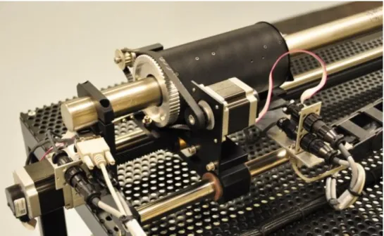
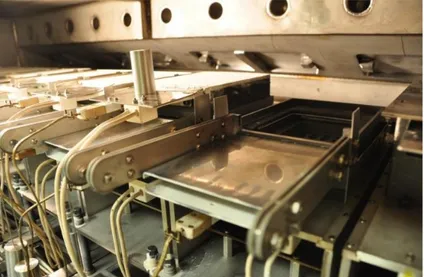
In the ARDS, a single substrate is transported by a magnetically coupled end effector. Linear transfer motion is achieved by a ball bearing lead screw driving the carriage assembly in Figure 3-5. The carriage is magnetically coupled to the transfer arm within the stainless tube. A rack and pinion gear mounted at the end effector converts rotational motion of the carriage, to linear motion of the end effector in Figure 3-6. The end effector is mounted on a precision guided transfer arm which moves linearly behind the deposition stations. At the desired station, the end effector is extended into the process station. The end effector is made of Inconel to inhibit
19
thermal and chemical degradation. The ARDS represents the longest automated magnetic transfer arm currently in operation according to the manufacturer, Transfer Engineering.
Figure 3-5: Magnetic coupling carriage assembly of the ARDS vacuum transfer arm; developed by Transfer Engineering.
Figure 3-6: ARDS load lock and end effector for substrate transport and manipulation. 3.6 Heated Pocket Deposition Source Design
Achieving predictable results requires maintaining a steady state condition within the process space. The primary factor affecting run length is material consumption via loss mechanisms. Material sublimation is sustained
20
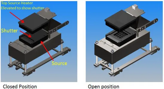
at elevated temperatures over the duration of an experiment, but material usage is managed by a novel shutter system. A passive shutter was conceived to close the sublimation sources between samples. The graphite shutters are actuated open by the translating end effector into the source, where the substrate becomes the target and receives the material vapor. As the substrate is withdrawn, a counter weight system closes the shutter and caps the source, preserving charge. The CAD model of the HPD source assembly in Figure 3-7 identifies the Top/Bottom sources and shutter. The physical hardware as installed in the ARDS is presented in
Figure 3-8, and with the top source removed to view pocket and shutter hardware in Figure 3-9.
Figure 3-7: Assembly view of ARDS HPD hardware with shutter in closed and open position.
21
Figure 3-9: Heated pocket deposition source revealing pocket and shutter hardware
Heating of the source material, and substrate, are by means of radiation heat transfer, requiring tight thermal uniformity. Careful design and analysis was performed to provide uniform and rapid heating of the sublimation crucible [31]. Graphite was selected for the source material based on having excellent thermal conductance and chemical inertness. Heating is accomplished by coiled Nichrome elements. The elements have been electrically isolated and cemented into the crucible with a ceramic compound as visible in Figure 3-10. This technique produces rapid uniform heating and minimizes the thermal influence on surrounding components. This heating technique also enables the precise placement of heating elements for tuning of thermal gradients. The embedded elements have enabled the stacked source geometry utilized in the co-sublimation source. The heating system is controlled by Watlow temperature controllers, communicating with high voltage solid state switching devices, and responding to k-type thermocouples located in the body of the crucible.
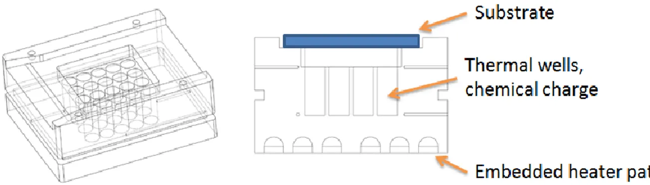
22
A section view of the bottom HPD source is presented in Figure 3-11. Photovoltaic material, of varying form, is placed in thermal wells within the source as demonstrated with CdS in Figure 3-12. The thermal wells provide additional radiating surface area to improve the uniformity of sublimation. Material forms include powder, granular, chucks, and slugs. The powder and granular material are pressed into the wells, increasing charge density and improving control of the sublimating surface area.
Figure 3-11: Sectional view of ARDS HPD bottom source, and substrate placement.
Figure 3-12: Bottom HPD source presenting CdS charge.
With the help of simple radiation heat transfer algorithms, the substrate and source temperatures can be approximated and tuned. Thermal control of the substrate is dominated by radiation heat transfer through the front side of the glass, opposite to the deposition surface, where the emissivity is largest through most of the process. During deposition, heat is transferred to the substrate by radiation and material transport. A heated top source is used to maintain the temperature of the substrate.
23
3.7 Heated shutterAs the shutter is displaced by the incoming substrate, it undergoes a drop in temperature. This reduced temperature allows condensation of source material, limiting run length and inhibiting motion. To control this deposition of material, an actively heated shutter was developed, Figure 3-13. Utilizing the previously defined method, an embedded heating element was integrated into the shutter, maintaining a deposition free temperature. A reduction in the material consumption and reliable actuation of the shutter resulted, increasing run lengths.
Figure 3-13: ARDS heated shutter hardware 3.8 Temperature measurement
As a means to monitor substrate temperature, provisions for pyrometers were installed behind each station, above the transfer galley, Figure 3-14. The pyrometer has a measurement range of 100-1300C, and emissivity adjustment of 0.2-1 at a spectral range of 5 micron. Calcium fluoride pyrometer viewports are utilized for their high IR transmission. The sample is rapidly scanned beneath the pyrometer providing a thermal profile of the process, while minimally impacting substrate temperature.
24
Source temperature is monitored with shielded k-type thermocouples installed within the body of the sublimation source. The location of measurements was determined from thermal modeling to be representative of the pocket temperature. Redundant TCs are installed for process security, and uniformity monitoring.
3.9 Process Control
In-situ characterization techniques are limited in the ARDS due to the high operational temperatures and high operating pressures. Precise control of key parameters including process pressure and composition, source and substrate temperature, and dwell time enable repeatable process results. Careful mapping of process parameters to device performance are highly valuable for process tuning. The ARDS is highly repeatable when maintained according the standard operating procedures (SOP). Rapid testing of film thickness and Voc during sample generation is useful to confirm process performance.
3.10 Integration and Startup
The shell of the system and many of the primary components were fabricated before this research was started. Final integration of pumping systems, source hardware, transfer mechanisms and process control were necessary prior to initial startup of the system. This research included the definition and execution of machine maintenance and modifications throughout the period of study. This included manufacturing new hardware and coordination of resources as necessary.
System startup began with atmospheric testing to address mechanical issues associated with substrate transfer and shutter actuation. Fine tuning of shutter components to correct clearances and alignment was necessary. Stainless galling was corrected by carful application of Boron Nitride to metal-metal interfaces, and utilization of high temperature ceramics where possible. Initially, the length of the transfer arm presented difficulties in maintaining repeatable positioning. Guiding mechanisms were inadequate to resist bending and rotational moments, occasionally interfering with source hardware. Modification to bearing assemblies and precision alignment of supporting structures has resulted in reliable motion.
Achieving quality vacuum required locating leaks by means of helium leak detection and correcting. The large number of feedthroughs, o-ring seals and chamber deflection frequently presented challenges in sealing. Baseline quantification of virtual leaks and outgassing of components assists in monitoring vacuum quality over the life of the system. Further mechanical testing under vacuum was performed to ensure component alignments were
25
maintained as deflection of the vacuum chamber occurred. Adjustments to pumping and venting systems were made to optimize operation and minimize process pressure variation.
With mechanical and vacuum testing complete, thermal testing was initiated. CSS operating temperatures in excess of 600C present a serious mechanical and thermal challenge. Further modification to hardware to account for and/or control thermal deflection was necessary. Managing chamber skin temperature was major challenge, as the radiation shielding was inadequate, and top sources relied upon radiation cooling to the skin. Extensive heat load at the front end of the process cause heating induced vacuum seal failure, and chamber distortion impacting substrate transfer. Internal radiation shields were developed and external heat management techniques were implemented to mitigate thermal issues. Additional alignment of the transfer arm at process temperatures was performed, correcting for thermal expansion of components. High voltage arcing due to insufficient electrical isolation frequently blew fuses and tripped breakers until corrective shielding was implemented. The original method of potting heater elements into sources caused separation of source and element under thermal cycling. A design change to incorporate a locking element was derived and corrected this failure.
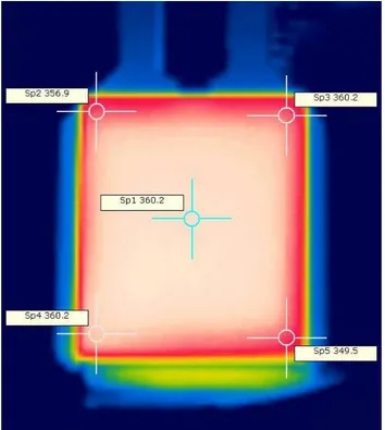
Testing of feedback and control loops was performed, ensuring systems were communicating correctly. Tuning of the PID heater control parameters was performed to achieve rapid heating, minimal overshoot and stable response. It was revealed that the potential for thermocouple failure, randomly or through maintenance activities, necessitated the installation of redundant thermocouples. A second source location was identified for the redundant measurement and further improved the understanding of source uniformity. Several studies were performed to measure heating rates, uniformity, and cross talk between sources. The results were used to improve and validate modeling efforts. Thermal characterization of the substrate uniformity was performed with an IR camera, and compared to the in-situ pyrometer. The thermal impact of the end effector is realized in Figure 3-15.
Satisfied with mechanical and thermal qualifications, the introduction of chemical was approved. Prior to the loading of chemical into the system, safety measures were to be addressed due to the handling of Cadmium compounds. The installation of a containment buddle seen in Figure 3-16, with HEPA filtration, and tacky mats served to contain chemical migration. Generating dedicated tool sets, including a HEPA vacuum, for performing maintenance was required to limit exposure of lab personnel. Configuring a portable fume hood for access from the containment bubble allowed chemical processing and loading of sources.
26
Figure 3-15: IR image of a substrate in the end effector after heating.
Figure 3-16: ARDS with containment and mini-environment.
The introduction of chemicals was done individually to monitor for migration and contamination. Films would be carefully characterized for material composition to ensure isolation of species. Routine testing of performance and process repeatability of devices with no copper was used to establish confidence in process control. Baseline films were produced for each species and catalogued as a means to identify contamination.
27
CHAPTER 4: PROCESS DEVELOPMENT AND DEVICE RESULTS
4.1 Methodology
Achieving device performance requires a strong correlation to processing conditions, but decoupling process and performance can be very challenging with CdTe cells. The development of the ARDS process required careful mapping of process parameters and performance metrics. Fortunately, the ARDS provides a highly tunable process, allowing individual parameters to be modified while maintaining the balance of process conditions. The process space for CdTe solar cells is very non-linear and requires concurrent tuning of all parameters. Strong interdependencies exist between the as deposited CdS/CdTe layers and the CdCl2 and Cu back contacting processes. Optimized individual parameters do not directly translate to an optimized complete device, as complex interactions result during junction formation and treatment. Establishing the baseline process to demonstrate 12% device efficiency required an extensive test methodology to understand device structure, process and performance. At the onset of chemical tuning, the strategy described in Table 4-1 was used as a guideline.
Table 4-1: ARDS experimental strategy for process development
The introduction of Cu would only be considered after a strong no-Cu performance resulting Voc>750mV was achieved. This restriction is due to the concern for high mobility of Cu within the system. Unintentionally introduced Cu at elevated temperatures or prior to effective CdCl2 treatment produces artificially improved device performance and poor stability.
28
4.2 Closed Space Sublimation BasicsClosed space sublimation (CSS) is a novel technique that has been used to produce many record cell efficiencies. The ARDS utilizes heated pocket deposition (HPD), a variation of CSS. HPD can be utilized for the sequential deposition of films to form the complete photodiode, providing an inline, single vacuum process. The primary benefits are the achievement of high deposition rates and material utilization, modest vacuum requirements, and simplicity of hardware. CSS is a high temperature technique by which a solid to vapor transformation occurs in an inert environment, transporting source material to a target as demonstrated in Figure 4-1, where it is re-condensed as a polycrystalline thin film [32]. Cruz-Campa presents a deposition rate model for CdTe deposition by close-space sublimation. As presented in Figure 4-2 and Figure 4-3, Cruz-Campa demonstrates the dependence of pressure and substrate temperature on the resulting deposition rates [33].
Figure 4-1: Close-space sublimation of CdTe [33]
The source material is produced in various forms, from powder to slugs, and is deposited in a heated source. At given pressure and gas composition, the source material will have a sublimation profile. The material is heated to a temperature for which a desired rate of sublimation occurs, and the material travels in the direction of diminishing partial pressure until it reaches a surface where deposition can occur or achieves a saturation pressure. This approach results in a high rate of non-equilibrium deposition that has the potential to induce significant intrinsic defects in the bulk of the film, limiting device performance [34]. Modification of the deposition dynamics can be achieved through source geometry, sublimation rate, and the deposition energy relating to substrate temperature. Deposition rates are dominated by the substrate temperature, and produce microstructural features based on the
29
growth rate. Condensation of particles on the substrate and resulting film formation are a function of sticking, diffusion, nucleation and growth. Management of intrinsic defects through process control results higher efficiency devices [35]
Figure 4-2: Exponential behavior of the estimated deposition rate vs. source temperature for different source– substrate separations. [33]
Figure 4-3: Estimated deposition rates vs. chamber pressure. The growth rate increases as pressure decreases in the diffusion-limited regime; in the sublimation-limited regime, the growth rate remains constant. [33]
30
4.3 Process SpaceUtilizing knowledge gained on the AVA system, and criteria from the Abound Solar process, a background gas composition of 2%O2 in N2 at 40mT was selected. For this environment, a starting source and substrate temperature profile was specified. Studies to produce a baseline process would systematically explore a large process space to achieve the target device parameters. Investigation of sequence, dwell times, process pressure and gas composition would be performed to increase understanding of process response, and device performance.
A Labview program was created to estimate the thermal profile of the substrate through the process. Input parameters for each process step included top and bottom source temperatures and emissivity, dwell time, and substrate emissivity for both the coated and uncoated side of the sample. With the substrate thickness, an algorithm determined the resulting heat transfer between source and substrate to produce the temperature profile of the substrate through the process, as presented in Figure 4-4
Figure 4-4: Predicted thermal profile of substrate. 4.4 Substrate Heating
At the onset of this research, a target substrate temperature of ~370C was demonstrated to produce suitable CdS film crystallography in the AVA system. The exit temperature of the substrate is critical to the nucleation of CdS and subsequent film morphology. The substrate exit temperature directly affects the CdS deposition dynamics. The strong interaction of process parameters is initially demonstrated by the substrate exit temperature. Further
31
tuning of the substrate heater is performed after the development of CdCl2 films to test thinner CdS, while maintaining exit temperature.
The open source geometry and high temperature of the heating station are well suited for thermal cleaning of the end effector between samples. Various dwell conditions were investigated to identify a condition resulting complete re-sublimation of chemical deposits from the end effector. A 440sec dwell was necessary to achieve a carrier temperature adequate to resublime CdS deposits, and is performed after every CdCl2 treatment.
The heating station is also used to perform reheating of previously deposited films, such as sputtered CdS:O prior to further deposition. Its proximity to the pyrometer allows precise tuning of substrate exit temperature. 4.5 CdS Optimization
Producing a sufficiently thin, high density CdS window layer is critical to achieving maximum potential Voc. Non-conformal coverage in the form of pinhole defects and gross discontinuities act as weak diode regions between the CdTe and TCO effectively reducing Voc [36] [29]. The method preferred for high growth rate CdS processing is CSS, typically resulting larger grain size and band gap than films grown by chemical bath deposition (CBD), an alternative method [37]. The large CdS grain structure produced with CSS can make achieving conformal coverage difficult, but careful substrate preparation and optimized deposition conditions improve nucleation and coverage.
To control the influence of pinhole defects, CdS films of 100-200nm thickness are necessary with standard substrates. To maximize Jsc, the CdS layer should be thinned just until a reduction in the voltage is observed. High temperature CdCl2 treatments drive the interdiffusion of CdS-CdTe, which serves to effectively reduce the thickness of the CdS layer. With aggressive treatments, the entire CdS layer can be consumed, creating a junction between the resulting CdTe1-xSx alloy and TCO [38].
Tuning of the process to achieve thin and dense films was performed as a first priority. To test the stability of the sublimation source, samples were generated at a constant temperature over a period of time after source replenishment. The data set presented in Figure 4-5 represents repetitive samples from a single run, and continued over successive runs. Sampling is not performed until source temperature has maintained steady state for 20minutes. The film thickness vs. time is exhibits an initial elevated sublimation rate, which stabilizes over an extended period of time. This observation demonstrated the need for a routine “burn-in” procedure after loading new CdS material. The “burn-in” procedure is performed by locking the shutter assembly open and placing a substrate directly on the
32
source to capture sublimated material. A temperature of ~640C is maintained for ~6hrs to burn off loose material, leaving a compact plug of material in the source.
Figure 4-5: Deposition rate resulting over cumulative run time
The next objective was to generate thickness vs. Temperature curves. Film deposition rates were determined empirically, targeting 60nm/min, using Design of Experiment (DOE) methodologies. Combinations of thermal profiles for source and substrate were performed, investigating deposition rates and resulting film quality. Maintaining all other process parameters, CdS bottom source temperature was swept over a temperature range. The resulting optical images in Figure 4-6, and thickness curves in Figure 4-7, represent a process space resulting films of ~50-300nm thickness. Films were measured using profilometry and compared to UV-vis results. The spectral dependence of transmission and absorption of CdS films with varying thickness are presented in Figure 4-8 and Figure 4-9. Samples were studied using blue light measurements to characterize pinhole density and results presented by Tashkandi [39].
33
Figure 4-7: CdS Thickness vs. Bottom source temperature; 3 Top temperatures presented
Figure 4-8: Transmission vs. Wavelength of varying thickness CdS films on 3mm TEC10 substrate.
Figure 4-9: Absorption vs. Wavelength for varying thickness CdS films on 3mm TEC10 substrate. y = 0.0925x2 - 105.92x + 30322 R² = 0.999 y = -0.005x 2 + 12.91x - 5890.9 R² = 0.9993 y = 0.065x2 - 72.57x + 20188 R² = 1 -50 0 50 100 150 200 250 300 350 400 450 580 590 600 610 620 630 640 650 CdS film th ickn es s (n m )
CdS Bottom Source Temperature (°C)
330 Top 410 Top 480 Top 0 20 40 60 80 100 400 450 500 550 600 650 700 750 % T Wavelength (nm) 3mm TEC 10 Only 40.4 nm; 580 C 73.5 nm; 600 C 139 nm; 620 C 233.7 nm; 640 C 311 nm; 660 C 0 20 40 60 80 100 400 450 500 550 600 650 700 750 % A Wavelength (nm) 3mm TEC 10 Only 40.4 nm; 580 C 73.5 nm; 600 C 139 nm; 620 C 233.7 nm; 640 C 311 nm; 660 C
34
Nucleation samples were generated at 10 second intervals using the target deposition rate. The correlation presented in Figure 4-10, provides an understanding of the linear relationship, and ability to produce varying film thickness without modifying source temperatures. Individual films were studied to investigate nucleation and growth characteristics in an attempt to improve resulting crystallographic properties. To ensure repeatable film thickness was achievable, samples were compared over 3 runs. The thickness curves are presented in Figure 4-11, and indicate a ±2.5C temperature variation for each setpoint tested. This confirmation allows rapid tuning of thickness for target device structures.
Figure 4-10: CdS Thickness vs. Deposition dwell time
Figure 4-11: CdS repeatability over three runs y = 1.8971x + 24.265 R² = 0.9939 0.0 50.0 100.0 150.0 200.0 250.0 0 20 40 60 80 100 120 C d S T h ic kn es s (nm )
Dwell Time (sec)
Note:
H1: 590/590 - 110sec
CdS: 400/640 - variable time
50 100 150 200 250 300 350 605 610 615 620 625 630 635 640 645 C d S T h ic kn es s (nm ) CdS Source Temp (°C) R033 R035_1 R035_02 Avg Expon. (Avg)Run ID
35
Early runs revealed the passive cooling of the top source was insufficient to test lower substrate temperature. New hardware to reduce thermal coupling of the top and bottom sources was implemented after the introduction of CdTe. Second generation top source hardware, having a larger radiation cooling surface, was subsequently installed achieving a reduction of the driven top source temperature from 370C to 325C. Investigation of films grown at the cooler temperatures produced very columnar grain structure and was deemed poor process space.
Through design of experiments (DOE) investigations of CdS-CdTe process interactions, several additional runs were generated to optimize POR CdS film. Higher substrate temperatures were required to achieve uniform film thickness and dense films. The baseline process, without plasma cleaning of the substrate, demonstrated a Voc cliff at ~110nm CdS as demonstrated in Figure 4-12. A typical CdS film on TCO is presented in Figure 4-13. Further optimization was achieved with the integration of a hollow cathode plasma source in the load lock for treatment of the substrate prior to deposition. A reduction in pinhole density of 95% [39] was observed with plasma cleaning, enabling thinner CdS films, resulting Jsc improvement while maintaining Voc.
Figure 4-12: J-V curves representing thinning of CdS on no-Cu devices. -25 -15 -5 5 15 25 35 -0.2 0.0 0.2 0.4 0.6 0.8 1.0
Cu
rr
e
n
t
De
n
si
ty
(m
A
/cm
2)
Voltage (V)
200nm CdS 165nm CdS 145nm CdS 110nm CdS 100nm CdS 85nm CdS 70nm CdS 30nm CdS200nm CdS
30nm CdS
36
Figure 4-13: SEM Micrograph (edge view) of typical ARDS CdS on TCO.
Additional runs were committed to produce specific CdS films supporting other research interests. (1)Development of Ellipsometry models for the optical measurement of CdS/CdTe solar cells [40]. (2)Intentional film defects and sample preparation methods for characterization by EL, PL, and blue light microscopy [23] [41]. (3)Investigation of reheating previously deposited CdS layers, either by CSS, sputtering or CBD for complete device fabrication. (4)Investigation of film and device properties resulting from the intermediate CdCl2 treatment of CSS CdS prior to CdTe deposition.
4.6 CdTe Optimization
Thickness control of the discrete layers is critical to maximum device efficiency. Optical techniques are commonly implemented for rapid non-destructive characterization, specifically material thickness. Optical properties of thin films can be dominated by the surface roughness, diminishing the precision and accuracy of measurement techniques [42]. Developing thickness profiles and correlating to key process parameters was performed. CdTe thickness correlations were generated by several techniques including XRF, SEM and primarily Profilometry.
Performing film analysis by XRF is a fast, non-destructive method. Kobyakov [43] demonstrated this technique for evaluating Cu treatments, which produces data for Cd and Te concurrently. Initially it was considered that this technique could serve dual purposes, monitoring Cu treatment and film measurement. The large area averaging technique does not account for grain density and surface texture, and therefore was determined to not have the accuracy necessary for process control. The early correlation is presented (Figure 4-14), but not used for further process development.
37
Figure 4-14: XRF correlation of Cd and Te counts to measured thickness (left), predicted growth rates using XRF trends (right)
It has been shown that the optimal properties of CdTe require only 2µm film thickness for better than 95% absorption of incident irradiation at 800nm. Developing a useful process space for producing ~2µm CdTe films and achieving quality CdTe microstructure, is essential to optimization of the CdCl2 treatment [44]. Maintaining other process parameters, CdTe thickness was correlated to the sublimation source temperature (Figure 4-15). While it has been shown that the substrate structure does not directly influence the structure of epitaxially grown CdTe films [45], CdTe films grown by CSS demonstrate a dependency to the deposition conditions [46].
Figure 4-15: CdTe thickness vs source temperature
The CdTe structure produced in the ARDS is dependent on substrate temperature during growth (Figure 4-16), likely affecting the nucleation and coalescence of grains [47]. While the exact mechanism is not well understood, there is a distinct relationship to between morphology and substrate temperature. Thornton [48] indicates three major zones (Figure 4-18) exist for micro-structural growth based on the processing conditions. Our findings are consistent with Thornton, and others relating substrate temperature to structure [49]. The three growth zones commonly referenced when discussing the morphology of thin films are defined as: (1) Zone 1 resulting
y = 0.0012x2 - 1.2462x + 322.51 R² = 0.9938 0 1 2 3 4 5 6 7 8 9 520 540 560 580 600 620 CdTe f ilm th ickn es s (u m )
38
tapered crystals with domed tops which are separated by void boundaries. Internal structure of the crystals is poorly defined, with a high dislocation density; (2) Zone 2 identified by columnar grains separated by distinct dense, intercystalline boundaries. The surface has a smooth, mat appearance; (3) Zone 3 producing equiaxed grains with a bright surface.
Figure 4-16: Process conditions resulting Low, Mid, and High substrate temperatures
Figure 4-17: SEM images of ARDS CdTe morphology at corresponding (a)Low, (b)Mid and (c)High substrate temperature.
39
Figure 4-18: Generalized micro-structural zones in PVD films as related to pressure and T/Tm. [48] [50] As a means to produce varying CdTe thickness, without adjusting the sublimation rate, the film thickness was compared to dwell time using a single source temperature (Figure 4-19). This was beneficial for investigation of CdTe thickness impact on the CdCl2 treatments, and ultimately the CdCl2 optimization for 2µm CdTe.
Figure 4-19: CdTe film thickness vs. deposition dwell time
As the process space for CdTe thickness was established, high surface roughness frequently resulted. The poorly coalesced grain structure and deep grain boundaries diminished the uniformity of CdCl2 treatment and
y = 0.013x + 0.0698 R² = 0.9983 0 0.2 0.4 0.6 0.8 1 1.2 1.4 1.6 0 20 40 60 80 100 120 C d Te Thi ckn e ss (u m)
Dwell Time (sec)
Note:
H1: 620/620 - 110sec CdS: 420/630 - 110sec CdTe: 420/555 - variable time
40
increased defects deep into the absorber layer. As identified by Sites [51], the primary causes of Voc loss in CdTe cells are a result of poor crystallinity. Others have also indicated the detrimental performance effects related to structural inhomogeneities emphasizing the need to improve the grain structure. [35]
As a first test, films were produced with various sublimation rates. The CdTe bottom source temperature was adjusted to achieve approximately .25, .5 and 1µm/min deposition rates, and the time interval adjusted to achieve the target film thickness. SEM was used to investigate the variation in microstructure. Cross sectional images are presented in Figure 4-20. These results confirm the 1µm/min growth rate was ideal for further development.
Figure 4-20: Cross sectional SEM images of CdTe microstructure resulting from different growth rates; visual appearance of the films are denoted above the image.
As the source shutter effectively maintains a closed condition of the source pocket, no gas exchange occurs except during sample ingress/egress. To increase the available O2 content during deposition, the source to sample
![Figure 1-3: Global annual new installed capacity of solar PV and wind, 2000-2011 [7]](https://thumb-eu.123doks.com/thumbv2/5dokorg/4335100.98387/11.918.228.694.104.411/figure-global-annual-new-installed-capacity-solar-wind.webp)
![Figure 1-5: Price forecasts of solar system; forecast with post 2008 curve. Figure reproduced from [7]](https://thumb-eu.123doks.com/thumbv2/5dokorg/4335100.98387/12.918.203.719.209.552/figure-price-forecasts-solar-forecast-curve-figure-reproduced.webp)
![Figure 1-9: Development of the space charge region for heterojunction solar cell. [14]](https://thumb-eu.123doks.com/thumbv2/5dokorg/4335100.98387/14.918.264.656.631.1034/figure-development-space-charge-region-heterojunction-solar-cell.webp)