Core Switching Noise for On-Chip
3D Power Distribution Networks
WAQAR AHMAD
Doctoral Thesis in Electronic and Computer Systems, KTH - Stockholm, Sweden, 2012.
ii
TRITA-ICT/ECS AVH 12:06 ISSN 1653-6363
ISRN KTH/ICT/ECS/AVH-12/06-SE ISBN 978-91-7501-519-4
© Waqar Ahmad, October 2012
KTH School of Information and Communication Technology, SE- 164 40 Kista, Sweden.
Thesis submitted to the School of Information and Communication Technologies, Department of Electronic Systems (ES), KTH Royal Institute of Technology, to be publicly defended on 2012-11-07 at 10:00 hrs in Stockholm, Kista.
iii
Abstract
Reducing the interconnect size with each technology node and increasing speed with each generation increases IR-drop and Ldi/dt noise. In addition to this, the drive for more integration increases the average current requirement for modern ULSI design. Simultaneous switching of core logic blocks and I/O drivers produces large current transients due to power distribution network parasitics at high clock frequency. The current transients are injected into the power distribution planes thereby inducing noise in the supply voltage. The part of the noise that is caused by switching of the internal logic load is core switching noise. The core logic switches at much higher speed than driver speed whereas the package inductance is less than the on-chip inductance in modern BGA packages. The core switching noise is currently gaining more attention for three-dimensional integrated circuits where on-chip inductance is much higher than the board and package inductance due to smaller board, and package. The switching noise of the driver is smaller than the core switching noise due to small driver size and reduced capacitance associated with short on-board wires for three-dimensional integrated circuits. The load increases with the addition of each die. The power distribution TSV pairs to supply each extra die also introduce additional parasitic. The core switching noise may propagate through substrate and consequently through interconnecting TSVs to different dies in heterogeneous integrated system. Core switching noise may lead to decreased device drive capability, increased gate delays, logic errors, and reduced noise margins. The actual behavior of the on-chip load is not well known in the beginning of the design cycle whereas altering the design during later stages is not cost effective. The size of a three-dimensional power distribution network may reach billions of nodes with the addition of dies in a vertical stack. The traditional tools may run out of time and memory during simulation of a three-dimensional power distribution network whereas, the CAD tools for the analysis of 3D power distribution network are in the process of evolution. Compact mathematical models for the estimation of core switching noise are necessary in order to overcome the power integrity challenges associated with the 3D power distribution network design. This thesis presents three different mathematical models to estimate core switching noise for 3D stacked power distribution networks. A time-domain-based mathematical model for the estimation of design parameters of a power distribution TSV pair is also proposed. Design guidelines for the estimation of optimum decoupling capacitance based on flat output impedance are also proposed for each stage of the vertical chain of power distribution TSV pairs. A mathematical model for tradeoff between TSV resistance and amount of decoupling capacitance on each DRAM die is proposed for a 3D-DRAM-Over-Logic system. The models are developed by following a three step approach: 1) design physical model, 2) convert it to equivalent electrical model, and 3) formulate the mathematical model based on the electrical model. The accuracy, speed and memory requirement of the proposed mathematical model is compared with equivalent Ansoft Nexxim models.
v
Acknowledgments
This thesis is published after four years of hard work which have contributed enormously towards my professional and technical growth. I express my deepest gratitude to the Department of Electronic, Computer, and Software Systems (ECS) of the School of Information and Communication Technologies (ICT) of KTH Royal Institute of Technology for the facilitation of this research work.
First of all, I would like to thank my advisor Prof. Hannu Tenhunen for his ease of cooperation: I would simply describe him as a person with the ability to quickly understand a problem and propose simple solutions. The best thing I liked about him was that he never imposed himself on me rather he helped my natural flow and encouraged every move in my studies and research. However, the initial journey towards PhD studies was complicated as I left my family back home and consequently had to return to settle some practical issues which required my attention. I am indebted to Hannu for being so positive and cooperative during the time of my return when I picked up the strings again. I most appreciate the guidance and support of Li-Rong Zheng, and Qiang Chen during my PhD studies. My thanks go to Dr. Roshan Weerasekera for his help during the beginning of my PhD studies when it was rather difficult to find the right way. I got a lot of inspiration and boosting from him as a senior member of the ELITE project. I am thankful to Awet Yemane Weldezion, Roshan Weerasekera, and all the others involved in the ELITE project for their useful company during the ELITE project meetings and workshops. I enjoyed the lunch time discussions with Prof. Hemani and other friends. Thanks to Prof. Elena Dubrova for her useful tips for my PhD studies.
I deeply acknowledge the sacrifices of my family and children during the course of my PhD studies. They always supported me through thick and thin. My situation dramatically improved after the arrival of my wife and children in Stockholm. I really picked up pace and moved in the right direction at that time. It was all possible because of love and care from my wife Khalida Waqar, my son Yahyea Waqar, my daughter Mariam Waqar, and the sweet addition of little baby Uzair Waqar.
I remember the cricket matches along with my fellow Pakistani PhD students during summer. It was great fun and entertainment which kept us
vi
all together. I am thankful to all my friends and families too numerous to mention here for giving me their dear company and support on the road towards my PhD.
I became seriously ill while writing the thesis when the finishing line was very close. I am grateful to all the doctors and nurses of Karolinska Hospital for their outstanding care and support. Thanks to my wife, for being there by the hospital bed to help me when I needed support to stand up. Special thanks go to Prof. Hannu Tenhunen, Prof. Axel Jantsch, and all others for managing the funding during that difficult time. I am also grateful to Alina Munteanu for her constant cooperation regarding the administrative matters.
Let me take this opportunity to admire the cooperation of the Swedish Institute (SI) and the Higher Education Commission (HEC) of Pakistan. I must pay tribute to HEC for the funding of my PhD studies and to SI for the support in my smooth stay here. I must also thank the travel grants support of
the FP7-ICT-215030 (ELITE) project of the 7th framework program.
Last but not the least I would also like to pay tribute to my employer organization for paying me a full salary, which made it financially possible to support my family in Stockholm.
Waqar Ahmad
September, 2012
vii
List of Publications included in the thesis
1. Ahmad W., Li-Rong Zheng, Qiang Chen, and Tenhunen, H., “Peak-to-peak Ground Noise on a Power Distribution TSV Pair as a Function of Rise Time in 3D Stack of Dies Interconnected through TSVs,” IEEE Transactions on Components, Packaging and manufacturing Technology, vol. 1, no. 2, pp. 196-207, March 2011.
2. Ahmad W., Qiang Chen, Li-Rong Zheng, and Tenhunen, H., “Modeling of Peak-to-peak switching Noise Along a Vertical Chain of Power Distribution TSV Pairs in a 3D stack of ICs Interconnected Through TSVs,” in Proceedings of IEEE NORCHIP Conference, pp. 1-6, November 2010.
3. Ahmad W., Qiang Chen, Li-Rong Zheng, and Tenhunen H., “Modeling of Peak-to-peak Core Switching Noise, Output Impedance, and Decoupling Capacitance along a Vertical Chain of Power Distribution TSV Pairs,” Springer’s Journal of Analog Integrated Circuits and Signal Processing (ALOG), vol. 73, no. 1, pp. 311-328, September 2012.
4. Ahmad W. et al., “Power Integrity Optimization of 3D Chips Stacked Through TSVs,” in Proceedings of IEEE Electrical Performance of Electronic Packaging and Systems Conference, pp. 105-108, October 2009.
5. Ahmad W., Kanth R.K., Qiang Chen, Li-Rong Zheng, and Tenhunen, H., “Power Distribution TSVs Induced Core Switching Noise,” in Proceedings of IEEE Electrical Design of Advanced Packaging and Systems Symposium, pp. 1-4, January 2011.
viii
6. Ahmad W., Kanth R.K., Qiang Chen, Li-Rong Zheng, and Tenhunen, H., “Fast Transient Simulation Algorithm for a 3D Power distribution Bus,” in Proceedings of IEEE Asia Symposium on Quality Electronic Design, pp. 343-350, August 2010.
7. Ahmad W., Qiang Chen, Li-Rong Zheng, and Tenhunen, H., “Peak-to-peak Switching Noise and LC Resonance on a Power Distribution TSV Pair,” in Proceedings of IEEE Electrical Performance of Electronic Packaging and Systems Conference, pp. 173-176, November 2010.
8. Ahmad W., Qiang Chen, Li-Rong Zheng, and Tenhunen H., “Decoupling Capacitance for the Power Integrity of 3D-DRAM-Over-Logic System,” in Proceedings of IEEE Electronics Packaging Technology Conference, pp. 590-594, April 2012.
9. Waqar Ahmad, and Hannu Tenhunen: Switching Noise in 3D Power Distribution Networks: An Overview, Chapter 10, pp. 209-224, Book VLSI Design, Edited by Esteban Tlelo-Cuautle and Sheldon Tan, Intech 2012, ISBN 978-953-307-884-7.
ix
Summary of Publications included in the thesis
Paper 1. A comprehensive mathematical model is developed in this paper in
order to investigate the behavior of power/ground noise as a function of the rise time for an inductive power distribution, TSV pair with decoupling capacitance. A TSV pair forming power and ground is modeled as a series RL circuit. The decoupling capacitance is modeled as a capacitor with small effective series resistance. The switching logic load connected to the power distribution TSV pair is modeled as a linear ramp current source. The switching noise is also modeled as a ramp function. The analysis is performed for the optimal design of the power distribution TSV pair to maintain a certain level of switching noise based on the worst case rise time.
Author’s Contributions: The author conceived the idea, performed modeling and simulation, and wrote the manuscript. To the author’s knowledge, so far there is no model available like this in the literature for the design of the power distribution TSV pair. The model is based on time domain analysis of noise. The model has +/- 5% deviation compared to Ansoft Nexxim. This model is simple to implement using Matlab. The proposed model provides guidelines for the physical design of a power distribution TSV pair based on the on-chip load requirements. In addition to this it is useful for optimal adjustment of power distribution TSV pair design and associated decoupling capacitance for specific load requirements.
Paper 2. In this paper an efficient and accurate model is proposed to estimate
the peak-to-peak core switching noise caused by simultaneous switching of logic loads along a vertical chain of the power distribution TSV pairs in a 3D stack of ICs.
Author’s Contributions: The author conceived the idea, performed modeling
and simulation, and wrote the paper. The model is accurate with 2-3%
deviation compared to Ansoft Nexxim. In addition to this, the model is 3-4 times faster than Ansoft Nexxim while requiring half of the memory. The proposed model is very useful for early estimation of the core switching noise along a chain of power distribution TSV pairs from bottom to top in a three-dimensional (3D) power distribution network. To the author’s knowledge, so far there is no model available like this in the literature for the vertical chain of the power distribution TSV pairs. The proposed model is flexible and takes into account the resistance, inductance, and capacitance of each TSV in the loop of switching current path. The model is proposed for n number of power
x
distribution TSV pairs in a vertical chain. Physical dimensions of each power TSV pair can be varied according to the requirement of the design. Values of resistance, inductance, and capacitance of pads, solder bumps, and interconnecting metallic lines can also be included in the model.
Paper 3. This paper is an extension of paper 2. In addition to the model, design guidelines for approximately flat output impedance for each stage of the vertical chain of power distribution TSV pairs are formulated. This is needed to realize the resonance free scenario over a wide operating frequency range.
The proper design of decoupling capacitance is a challenging issue in order to maintain the output impedance equal to or less than the target impedance for each tier of a three-dimensional (3D) power distribution network. Author’s Contributions: The author conceived the idea, performed modeling and simulation, and wrote the manuscript. The proposed design guidelines are useful for the selection of the value of decoupling capacitance along with effective series resistance (ESR), and effective series inductance (ESL) for each stage of the chain of power distribution TSV pairs. First of all the target impedance for each stage of the vertical chain of power distribution TSV pairs is determined according to allowed ripple and load at each stage. An equation is given to estimate the output impedance. The output impedance should be kept less than or equal to the target impedance. There are separate equations for the estimation of ESR and ESL for the decoupling capacitance. Finally, an equation is given for the estimation of the value of decoupling capacitance. The proposed technique is applicable to a large three-dimensional (3D) power distribution network containing multiple tiers, and multiple vertical power distribution chains.
Paper 4. A mathematical model for the estimation of core switching noise within a three-dimensional (3D) stack of dies interconnected through power distribution TSV pairs is proposed in this paper. The core switching noise in this model is a function of the value of resistance, inductance, and capacitance of the power distribution TSVs. In addition to this, the switching noise also depends on the value of the rise time, and amount of the logic load. The proposed model has +/- 3% deviation compared to an equivalent SPICE model. The proposed model is flexible and can be applied to uniform or
non-xi
uniform three-dimensional (3D) power distribution network. The proposed model can easily be solved for unknown voltages using Matlab. The known and unknown voltages along with RLC values of TSVs, RLC values of power distribution grid, logic load associated with each node, decoupling capacitance associated with each node, and rise time of the clock are put together in the form of matrices. The model is solved for unknown voltages using the direct method of solution in Matlab.
Author’s Contributions: The author performed modeling and simulation, and wrote the paper. The proposed model is applicable to any number of power distribution TSVs according to logic load requirements. The pattern of power distribution TSV pairs can also be changed according to on-chip area constraints.
Paper 5. This paper is based on extended analysis of the model proposed in
paper 4. The logic dies are interconnected using a single power distribution TSV pair in the center of each die for a 1mmx1mm grid in this paper and TSVs are placed along the periphery of the chips in paper 4. The behavior of core switching noise is investigated by adding dies in the vertical stack. The behavior of core switching noise is also investigated by increasing the clock frequency when only two dies are interconnected through a single power distribution TSV pair. The analysis is useful for early design tradeoffs for the design of a three-dimensional (3D) power distribution network.
Author’s Contributions: The author performed modeling and simulation, and wrote the paper.
Paper 6. Extensive transient simulations for on-chip power distribution
networks are required to analyze power delivery fluctuations caused by dynamic IR and Ldi/dt drops. Speed and memory has become a bottleneck for simulation of power distribution networks in modern VLSI design where clock frequency is of the order of GHz. The traditional tools are very slow and require a lot of memory resources for simulation. The problem is further aggravated for huge networks like power distribution networks within a stack of ICs inter-connected through TSVs. This type of 3D power distribution network may contain billions of nodes at a time. This paper presents a fast transient simulation algorithm for the 3D power distribution bus. The proposed algorithm uses a combination of mathematical techniques and
xii
visual C++ to reach a fast solution of the three-dimensional (3D) power distribution bus for voltage at each node. The branches at each node of the 3D power distribution bus are converted to a combination of resistance in series with the current source, using the trapezoidal rule. The star network obtained
this way is converted to the corresponding
π
network for each node of the 3Dpower distribution bus. This network is reduced to a single
π
network usingC++ reducing code. The reduced network is solved using nodal analysis i.e.
the network is converted to a matrix equation containing unknown voltages and currents. The system of matrix is solved for unknowns using the direct
method of solution in Matlab. Now,
π
network is back-solved for each nodeusing C++ back solution code. The proposed algorithm has +/- 1 to 2%
deviation compared to Ansoft Nexxim4.1. The proposed algorithm is several times faster than Ansoft Nexxim and also requires significantly less memory than Ansoft Nexxim. The speed is improved and less memory is required because of a significant reduction in the number of nodes compared to Ansoft Nexxim as shown by Table 5.5. The advantage in speed compared to Nexxim is also gained by converting the inductance and capacitance of each branch to the corresponding resistive element. The accuracy is achieved by means of an efficient algorithm using C++.
Author’s Contributions: The author conceived the idea, performed modeling and simulation, and wrote the paper. The model overcomes the speed and memory bottlenecks which is a prime concern because of the large size of the 3D power distribution network.
Paper 7. The core switching noise and LC resonance vary by varying different
circuit parameters of the power distribution TSV pair for a three-dimensional (3D) power distribution network. Variation of circuit parameters such as effective resistance, effective inductance, and the damping factor of the power distribution TSV pair affect the core switching noise and LC resonance. The variation of LC resonance vs. time is explored in this paper. The analysis shows that the magnitude of the transient term reduces by increasing the effective resistance of the TSV pair. Specifically, the peak of the transient term reduces by adding decoupling capacitance. Reducing effective inductance of the TSV pair not only reduces the peak of the transient term but also reduces the lasting time of the transient term.
The analysis shows 4-5% variation compared to an equivalent Ansoft Nexxim model. The analysis is useful for choosing the design of power
xiii
distribution TSV pair to control the magnitude and lasting time of the transient term as a result of the switching logic load.
Author’s Contributions: The author conceived the idea, performed modeling and simulation, and wrote the paper.
Paper 8. The three-dimensional (3D)-DRAM-Over-Logic system is one of the
promising applications of three-dimensional (3D) integration technology. It can be a vibrant technique to overcome memory wall and bandwidth wall problems. This paper considers a three-dimensional (3D) stack containing two DRAM dies over a single processor die. Placing decoupling capacitance on DRAM dies saves useful area on the processor die to increase the integration density in order to make full use of the bandwidth offered by TSVs in the vertical direction. The assumption is that decoupling capacitors are placed on each DRAM die and connected to power distribution TSV pairs passing through the DRAM stack.
The proposed mathematical model determines the optimum value of the decoupling capacitance on each DRAM die along with the optimum values of the effective resistance of the interconnecting power distribution TSV pairs. The proposed model has +/- 1.1% deviation compared to an equivalent Ansoft Nexxim model. The proposed model is flexible and useful for efficient budgeting of the amount of decoupling capacitance placed on DRAM dies. Author’s Contributions: The author conceived the idea, performed modeling and simulation, and wrote the paper. To the author’s knowledge, so far this is the first mathematical model for efficient budgeting of decoupling capacitance and physical design of the power distribution TSV pairs for a 3D-DRAM-Over-Logic System.
Book Chapter. We presented an overview and state of the art of switching noise for three-dimensional (3D) stacked integrated circuits in the form of a book chapter.
Author’s Contributions: It is written by author along with Prof. Hannu Tenhunen. The chapter provides brief state of the art knowledge about switching noise in 3D stacked power distribution networks.
xv
List of Publications not included in the thesis
1. Rajeev Kumar Kanth, Waqar Ahmad, Yasar Amin, Pasi Liljeberg, Li-Rong Zheng, and Hannu Tenhunen, “Analysis, Design and Development of Novel, Low Profile 2.487 GHz Micro strip Antenna” in Conference Proceedings of 14th International Symposium on Antenna Technology and Applied Electromagnetic and the American Electromagnetic Conference (ANTEM/AMEREM), Ottawa, Canada, pp. 1-4, August 2010.
2. Rajeev Kumar Kanth, Waqar Ahmad, Subarna Shakya, Pasi Liljeberg, Li-Rong Zheng, and Hannu Tenhunen, “Autonomous Use of Fractal Structure in Low Cost, Multiband and Compact Navigational Antenna” in Proceedings of IEEE Mediterranean Microwave Symposium (MMS), Northern Cyprus, pp. 135-138, October 2010.
3. Muhammad Adeel Ansari, Waqar Ahmad, Qiang Chen, and Li-Rong Zheng, ”Diode Based Charge Pump Design using 0.35um Technology ,” in Proceedings of IEEE NORCHIP Conference, Tampere, Finland, November 2010.
4. Muhammad Adeel Ansari, Waqar Ahmad, and Svante R. Signell, ”Single Clock Charge Pump Designed in 0.35um Technology,” in Proceedings of IEEE MIXDES, Gliwice, Poland, pp. 552-556, September 2011.
5. Waqar Ahamd, Qiang Chen, Roshan Weerasekera, Hannu Tenhunen, and Lirong Zheng, “Power Integrity Issues in 3D Integrated Chips Using TSVs (Through-Silicon-Vias),” 3D Integration Workshop, Design, Automation, and Test in Europe (DATE) Conference, Nice - France, pp. 274-275, April 2009.
http://www.date-conference.com/files/file/09-workshops/date09-
xvi
6. Waqar Ahamd, and Hannu Tenhunen, “Power Integrity Estimation of 3D Integrated Chips,” in Workshop Notes, Design, Automation, and Test in Europe (DATE) Conference, Dresden, Germany, pp. 357-360, March 2010.
http://www.date-conference.com/files/file/10
xvii
List of Figures
Fig. 1.1 A vision of future three-dimensional (3D) hyper-integration of
information technology, nanotechnology, and biotechnology systems, a new
paradigm for future technologies [5]...3
Fig. 2.1 The memory chip stacking by Samsung [38]...17
Fig. 2.2 Die-to-Die (D2D) stacking approaches: (a) Die-to-Die wire bonding. (b) Die-to-Die TSV bonding [24]...18
Fig. 2.3 Die-to-Wafer (D2W) stacking [41]...19
Fig. 2.4 (a) Wafer-to-Wafer stacking. (b) A defective die may stack to good dies thereby reducing the yield in Wafer-to-Wafer stacking...19
Fig. 2.5 Face-to-Face (F2F) bonding [44]...20
Fig. 2.6 Face-to-Back (F2B) bonding [44]...21
Fig. 2.7 Back-to-Back (B2B) bonding [44]...21
Fig. 2.8 Via-first TSV technology [44]...22
Fig. 2.9 Via-last TSV technology [44]...22
Fig. 2.10 Dies inter-connected through bonding wires [11]...23
Fig. 2.11 The dies interconnected through micro-bumps [11]...24
Fig. 2.12 Cross section of three-dimensional (3D) power distribution network having three planes and a TSV pair...24
Fig. 2.13 Top view of a 3D power distribution network [47]...25
Fig. 2.14 3D integration of nano photonics and CMOS using Cu-Nails (TSVs) [48]...25
Fig. 2.15 Electro-static coupling through on-chip capacitors [12]...26
Fig. 2.16 Electro-magnetic coupling through on-chip inductors [12]...26
Fig. 3.1 Equivalent electrical model of a decoupling capacitance, where ESR is effective series resistance and ESL is effective series inductance of decoupling capacitance...27
Fig. 3.2 V-curve showing impedance of the decoupling capacitance vs. frequency [49]...28
xviii
Fig. 3.3 (a) Frequency response of the impedance of a power distribution network without decoupling capacitance. (b) Frequency response of the impedance of a power distribution network with decoupling capacitance
[49]...30
Fig. 3.4 Distinctive peak of output impedance of a power distribution network due to anti-resonance [49]...31
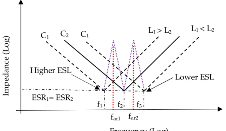
Fig. 3.5 Anti-resonance of two equal value parallel decoupling capacitors i.e. far1<far2 as far1 occurs when L1 > L2, and far2 occurs when L1 < L2 [52]...32
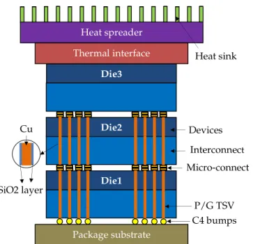
Fig. 4.1 Three dies forming a three-dimensional (3D) system with face-to-back bonding through micro-connects. Power is supplied through vertical TSV pairs from the package substrate [29]...35
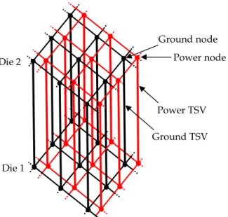
Fig. 4.2 3X3 orthogonal global supply grids of two neighboring dies in a 3D stack inter-connected through TSVs where red color indicates the power grid and black color indicates the corresponding ground grid...36
Fig. 4.3 Physical model of a power distribution TSV pair with the logic load and decoupling capacitance...36
Fig. 4.4 Schematic presentation of the on-chip current definition for CMOS [63]...39
Fig. 4.5 The shape of the on-chip logic switching current where ts is switching time...40
Fig. 5.1 Block diagram of a typical power distribution network for an integrated circuit [22]...45
Fig. 5.2 Hierarchical Model [79]...47
Fig. 5.3 4X4 RLC power grid model of a typical System-on-Chip...48
Fig. 5.4 Power Distribution node [86]...48
Fig. 5.5 Chip-Package-Board hierarchy of a typical three-dimensional (3D) power distribution network...49
Fig. 5.6 Electrical model of decoupling capacitance placed on DRAM dies in a
3D-DRAM-Over-Logic System. Vdd =supply voltage,
eff p
R = effective resistance
of package,Cdec1= decoupling capacitance on top DRAM die,
V
dec1= voltageacross Cdec1,
eff TSV
xix
decoupling capacitance on bottom DRAM die,
V
dec2= voltage across2
dec
C , eff TSV
R 2=2RTSV2= effective resistance of second TSV pair,VL= voltage across
logic load, and IL= equivalent current drawn by logic load...51
Fig. 5.7 Value of Vdec2vs. value of Cdec2for different values of Cdec1when
Ω
= m
Reff
TSV2 50 , Imax=3mA, and
t
r=100pS...55Fig. 5.8 Value of Vdec2vs. value of
eff TSV
R 1for different values of
1
dec
C
whenReff = mΩTSV2 50 , Cdec2=1pF, Imax=5mA, and
t
r=50pS...55Fig. 5.9 Value of VLvs. value of Cdec2for different values of
r
t whenReff = mΩ
TSV2 50 ,R = mΩ
eff
TSV1 100 , Cdec1=1pF, and Imax=5mA. Assume 10%
ripple in load voltage...56
Fig. 5.10 Electrical model of 3D power distribution bus having n nodes...57
Fig. 5.11 Equivalent bus consisting of trapezoidal Norton companion models
at each node...57
Fig. 5.12 Star to
π
conversion model at a node...58Fig. 5.13 Equivalent
π
model of a 3D bus after applying reductionalgorithm...58
Fig. 5.14 3X3 orthogonal global supply grids of two neighboring dies in a 3D
stack inter-connected through TSVs where red color indicates the power grid and black color indicates the corresponding ground grid...61
Fig. 5.15 Vertical power distribution TSV chains...63
Fig. 5.16 Electrical model of a vertical chain of n power distribution TSV pairs,
interconnecting n chips in a 3D stack of ICs...67
Fig. 5.17 Equivalent electrical model of a power distribution TSV pair with logic load and decoupling capacitance...69
Fig. 5.18 Clock and corresponding current and noise in time domain...70
Fig. 5.19 Peak-to-peak ground noise comparison of model from equation
(5.28) to the equivalent model in Ansoft Nexxim4.1, as a function of rise time forIp 3.3mA sw = ,L 50pH eff TSV = , R = 250. Ω eff TSV , R =75mΩ eff
dec , Cdec =5pF, and n
t
xx
Fig. 5.20 Part of switching current supplied by decoupling capacitance as a function of rise time for Ip 3.3mA
sw = , L 50pH eff TSV = , R = 250. Ω eff TSV , R =75mΩ eff dec , pF 5 Cdec = , and t=tn...73
Fig. 5.21 Part of switching current drawn from power supply as a function of
rise time for Ip 3.3mA
sw = , L 50pH eff TSV = , R =0.25Ω eff TSV , R =75mΩ eff
dec , Cdec=5pF, and n
t
t= ...74
Fig. 5.22 Peak-to-peak ground noise for different values of eff
TSV R for Ip 3.3mA sw= , pH 50 Leff TSV = , R =75mΩ eff
dec ,Cdec=5pF, and t=tn...77
Fig. 5.23 Peak-to-peak ground noise for different values of
eff dec R forIp 3.3mA sw= ,L 50pH eff TSV = , R =0.25Ω eff TSV ,Cdec=5pF, andt=tn...78
Fig. 5.24 Peak-to-peak ground noise reduction comparison by doubling the
value of decoupling capacitance and by halving the value of TSV effective parasitic inductance...79
Fig. 5.25 Vertical chain of n power distribution TSVs pairs interconnecting n
dies in a 3D stack. The power TSVs are in the red dotted box and the corresponding ground TSVs are in the black dotted box...80
Fig. 5.26 Electrical model for a vertical chain of n power distribution TSV pairs...81
Fig. 5.27 The equivalent electrical model of a single power distribution TSV pair along with logic load and decoupling capacitance, where IL1
( )
t is thecurrent drawn by the logic load, eff
P Z
1 is the effective output impedance across
the load...82
Fig. 5.28 Plot obtained using (5.37), showing the magnitude of the normalized
output impedance vs. normalized frequency for different values of
1 L U for = 1 R U 1 1 = TSV Q ...85
Fig. 5.29 The plot obtained through (5.41), showing the magnitude of the normalized output impedance vs. the normalized frequency for different values ofQTSV1, for critically damped system...86
Fig. 5.30 The plot obtained through (5.42), showing the magnitude of the normalized decoupling capacitance vs. UR1 andUL1...87
xxi
List of Tables
Table 1.1 Classification of circuit size from 1963-2010 [1]...1
Table 1.2 Intel Desktop Processor Trends for the last ten years
[2]...4
Table 1.3 ITRS 2011 predictions about high volume microprocessors for the next decade [1]...4
Table 1.4 Comparison amongst different design approaches [14]...6
Table 1.5 Comparison amongst three-Dimensional (3D) assembly
technologies [14]...6
Table 1.6Comparison of size and interconnect density between 3D IC and 3D
SOP [16]...7
Table 1.7 Design challenges roadmap for 3D integration technology
[1]...8
Table 1.8 3D Interconnect Hierarchy Roadmap [1]...9
Table 1.9 Emerging Global Interconnect Level 3D-SIC/3D-SOC Roadmap for
TSVs [1]...9
Table 1.10 Emerging Intermediate Interconnect Level 3D-SIC Roadmap for
TSVs[1]...10
Table 4.1 TSV dimensions used for analysis...43
Table 5.1 Optimization of decoupling capacitance on both the DRAM dies
based on the effective resistance of the TSV pairs, assuming 10% ripple to be allowed in the voltage across the load with the minimum value of Vdec2to be equal to 0.92V...53
Table 5.2 Dependence of decoupling capacitance placed over DRAM dies on
power distribution TSV pair’s resistance. Assume 10% ripple is allowed in voltage across load...54
Table 5.3 Comparison of the proposed algorithm with Ansoft Nexxim for
CPU time (Sec)...58
Table 5.4 Comparison of the proposed algorithm with Ansoft Nexxim for
xxii
Table 5.5 Comparison of the proposed algorithm with Nexxim for node
reduction...60
Table 5.6 Simulation time comparison of proposed model with Ansoft
Nexxim4.1 by increasing the number of TSV pairs in vertical chain, for RTSV=0.25 ohm, LTSV=50 pH, CLoad=500pF, and Cd=5pF. Nodes are numbered
from bottom to top...68
Table 5.7 Memory requirement comparison of proposed model with Ansoft
Nexxim4.1 by increasing the number of TSV pairs in vertical chain, for RTSV=0.25 ohm, LTSV=50 pH, CLoad=500pF, and Cd=5pF. Nodes are numbered
from bottom to top...68
Table 5.8 peak-to-peak ground noise comparison of (5.28) model with
equivalent model obtained through Nexxim4.1 for worst case rise time by varying values of effective inductance of TSV pair forIp 3.3mA
sw = ,R 0.25 eff TSV = Ω , Ω = 0.075 Reff
dec , and Cdec=5pF...74
Table 5.9 Peak-to-peak ground noise comparison of (5.28) model with
equivalent model obtained through Nexxim4.1 for worst case rise time by varying values of effective resistance of TSV pair and effective series resistance of decoupling capacitor for Ip 3.3mA
sw = ,L 50pH eff
TSV = , andCdec =10pF..76
Table 5.10 Peak-to-peak ground noise comparison of (5.28) model with
equivalent model obtained through Nexxim4.1 for worst case rise time by
varying values of decoupling capacitance for Ip 3.3mA
sw = ,R 0.25 eff TSV= Ω , Ω = 0.075 Reff dec , andL 50pH eff TSV = ...76
Table 5.11 Peak-to-peak ground noise reduction for different values of the
rise time by increasing the value of decoupling capacitance
forIp 3.3mA sw= ,L 50pH eff TSV = ,R =0.25Ω eff TSV , R =75mΩ eff
dec ,Cdec=5pF and t=tn...77
Table 5.12 Peak-to-peak ground noise reduction for different values of the rise time by decreasing the value of TSV effective inductance forIp 3.3mA
sw= ,Cdec=5pF,R =0.25Ω eff
TSV , R =75mΩ eff
xxiii
Abbreviations
3D: Three-Dimensional.
2D: Two-Dimensional.
IR drop: Voltage drop caused by resistance of the circuit due to current load.
Ldi/dt noise: Noise caused by inductance of the circuit due to switching of
load.
TSV: Through-Silicon-Via.
I/O: Input/Output.
GHz: Gigahertz.
BGA: Ball Grid Array.
CAD: Computer-aided Design.
DRAM: Dynamic Random Access Memory.
ps: pico-second.
um: micro-meter.
nm: nano-meter.
PDN: Power Distribution Network.
IC: Integrated Circuit.
PCB: Printed Circuit Board.
P/G: Power/Ground.
ITRS: International Technology Road Map for Semiconductors.
ULSI: Ultra Large Scale Integration.
HCI: Hot Carrier Injection.
NBTI: Negative Bias Temperature Instability.
CMOS: Complementary Metal Oxide Semiconductor.
xxiv
NMOS: N-channel Metal Oxide Semiconductor.
PMOS: P-channel Metal Oxide Semiconductor.
AC: Alternating Current.
RLC: Resistance, Inductance, and Capacitance.
ESR: Effective Series Resistance.
ESL: Effective Series Inductance.
CPU: Central Processing Unit.
nH: nano-Henry.
DC-DC: Direct Current to Direct Current.
D2D: Die-to-Die.
KGD: Known Good Dies.
D2W: Die-to-Wafer.
W2W: Wafer-to-Wafer.
F2B: Face-to-Back.
B2B: Back-to-Back.
F2F : Face-to-Face.
FEOL: Front End of Line.
BEOL: Back End of Line.
LC: Inductance, and Capacitance.
xxv
Table of Contents
Abstract... iii Acknowledgements ... v
List of publications include in the thesis ... vii Summary of publications included in the thesis ... ix
List of publications not included in the thesis ... xv List of Figures ... xvii List of Tables ... xxi Abbreviations ... xxiii
1. Overview...1
1.1 Motivation for Three-Dimensional Integration ... 4 1.2 Challenges to Three-Dimensional Integration ... 7 1.3 Road Map for 3D Interconnects ... 9
1.4 Thesis Contribution and Objectives ... 10 1.4.1 Contribution...10 1.4.2 Objectives...13
1.5 Overview of the Thesis Structure ... 14
2. Structures for 3D Integration ...17
2.1 Three-Dimensional Stacking Approaches ... 18 2.1.1 Die-to-Die (D2D) Stacking ... 18 2.1.2 Die-to-Wafer (D2W) Stacking ... 18
xxvi
2.2 Three-Dimensional Bonding Approaches ... 19 2.2.1 Face-to-Face (F2F) Bonding ... 20 2.2.2 Face-to-Back (F2B) Bonding ... 20
2.2.3 Back-to-Back (B2B) Bonding ... 20 2.3 Three-Dimensional TSV Approaches ... 22 2.4 Three-Dimensional Vertical Interconnect Approaches ... 23
3. On-Chip Decoupling Capacitance ...27 3.1 Impedance of the Decoupling Capacitance ... 27
3.2 Impact of Decoupling Capacitance on Target Impedance ... 29 3.3 Anti-resonance and parallel decoupling capacitors ... 31 3.4 Effective On-Chip Decoupling Capacitance ... 33
4. Core Switching Noise for 3D PDN ...35 4.1 Core Switching Noise ... 37
4.2 Modeling of the Core Switching Noise ... 39 4.3 Toward a Robust 3D PDN Design ... 42
5. Modeling of On-Chip Power Distribution Networks ...45 5.1 Modeling Approaches ... 46
5.1.1 Finite Difference Time Domain (FDTD) Method ... 46 5.1.2 Latency Insertion Method (LIM) ... 46 5.1.3 Hierarchical Modeling Method ... 46
5.1.4 Distributed RLC Model for Power Grid ... 47 5.1.5 Compact Physical Modeling for GSI Power Distribution Grids ... 48
xxvii
5.1.6 Combined Chip-Package-Board Modeling ... 49 5.2 Previous Work and Thesis Contribution ... 49
6. Summary and Future Work ...91 6.1 Summary...91 6.2 Future Directions...92
References...95
xxviii
Overview 1
Chapter 1
Overview
The small scale commercial production of integrated circuits started in the early 1960’s. In 1965, Gordon Moore predicted the transistor density would double every 18 to 24 months, which became known as Moore’s Law. After that the transistor density increased due to increased demand for small size in hand-held devices, System-on-Chip (SoC), and the defense industry. The modern day integrated circuits may have billions of transistors, as shown in Table 1.1 [1].
Table 1.1 Classification of circuit size from 1963-2010 [1].
Year Integration Level Transistor Count
1963 Small Scale Integration (SSI) <100
1970 Medium Scale Integration (MSI) 100-300
1975 Large Scale Integration (LSI) 300-30000
1980 Very Large Scale Integration (VLSI) 30000-1 million
1990 Ultra Large Scale Integration (ULSI) >1 million
2010 Giga Scale Integration (GSI) >1 billion
The functionality comes by reducing the size of the transistors and also by increasing the transistor count per unit area of the processor die. More transistors are added to processors with each technology node as shown in Table 1.2 [2]. Speed or frequency of the processor is also increased with the passage of time in order to make full use of the functionality and resources. The transistor current density increases with each technology node. The capacitance of transistors reduces by decreasing the size. The power consumption should reduce due to reduction of voltage with each technology node but power consumption actually increases due to increase in frequency of the processor as shown in Table 1.2 [2].
There is a demand for increased chip size, and an increased number of I/O pins, which results in increased power dissipation due to increased speed and increased transistor count in future as shown in Table 1.3 [1]. System-on-Chip (SoC) was introduced in order to integrate all the components on a single substrate. SoC has incredible functionality having processor, digital logic, memory, embedded intelligence, and analog components on a single die. However, interconnect length is a critical issue for SoC due to increase in the chip dimensions. Mixed signal integration is another issue for present-day SoC as the noisy digital part cannot be placed in close proximity to the sensitive analog part. In addition to this, same technology node has to be followed for different components of SoC which may place stringent requirements on analog and RF components. Three-dimensional (3D)
Overview 2
integration with TSVs is, therefore, an obvious choice for mixed technology applications compared to SoC.
The inductance of on-chip power distribution grid causes ground bounce due to fast switching transistors. The simultaneous switching of I/O drivers also changes the voltage level of the power lines due to inherent inductance of the power distribution network. The overall effect of all these factors degrades the signal-to-noise ratio of integrated circuits. With the present advancements in semiconductor technology, the chip supply voltage has reached 0.9 V, maximum allowable power has reached 158 W, and frequency is of the order of GHz [1]. Complexities associated with all these developments are increased di/dt noise, reduced voltage margins, and increased IR-drop. On-chip inductance becomes significant at high frequencies and causes voltage fluctuations in the power distribution grid. These voltage fluctuations are in the form of overshoot or undershoot in power supply rails. An overshoot in the power rail (or undershoot in the ground rail) causes overstress in transistor gate-oxide or excessive charge/discharge in power distribution network nodes [3]. Conversely, undershoot in the power rail (or overshoot in the ground rail) reduces noise margins of the transistors causing poor driving capabilities [3]. The parasitic associated with long power distribution rails becomes a key issue under these circumstances.
Nowadays, there are many embedded or invisible devices in the environment. Some of these devices are context-aware i.e. they know about their state or situation. Some of the devices can be personalized or tailor-made to the user’s needs and can recognize the user. Sometimes the devices are adaptive i.e. can change response to the environment or an event. All this leads to More than Moore’s law which is meant to interact with the user and environment. More than Moore’s law is to serve the ambient intelligence requirements i.e. sensitivity and response to human needs and presence. There was a buzz for “More than Moore’s Law” with the introduction of System-on-Package (SoP) technology. The real movement for “More than Moore’s Law” started with the arrival of three-dimensional (3D) integration technology which tends to focus on system integration. The More than Moore’s approach typically allows for non-digital functionalities such as sensors, actuators, power control, and radio frequency communication [4]. Three-dimensional (3D) integration technology is a strong candidate for More than Moore’s law. The anticipated applications of 3D integration include memory, portable devices, high performance computers, and
high-density multifunctional heterogeneous integration of information technology,
nanotechnology, and biotechnology systems as shown in Fig. 1.1 [5].
The purpose of 3D integration is either to partition a single chip into multiple strata to reduce global interconnect length or stacking of chips together using TSVs [6]. Increasing the number of strata from one to four reduces the length of the longest interconnect by 50% with 75% improvement in latency and 50% improvement in interconnect energy dissipation
Overview 3
[7]. Using three-dimensional integration, the clock frequency can be increased by 3.9X and area and power can be reduced by 84% [6]. Energy dissipation of long on-chip wires can be reduced by 54% by using three-dimensional interconnects in a 45nm technology node [8]. Three-dimensional integration provides the potential for a tremendously increased level of integration per unit footprint compared to its two-dimensional (2D) counterpart [9].
Fig. 1.1 A vision of future three-dimensional (3D) hyper-integration of information
technology, nanotechnology, and biotechnology systems, a new paradigm for future technologies [5]. Power Processor Memory Stack RF ADC DAC Nano Device MEMS Other Sensors, Imagers Chemical and Bio Sensors
Overview 4
Table 1.2 Intel Desktop Processor trends for the last ten years [2].
Year Model Process Clock Transistor Count Max. TDP
1993 Pentium 0.8um 66 MHz 3.1 million 8W
1995 Pentium Pro 0.6um 200 MHz 5.5 million 15.5W
1997 Pentium II 0.35um 300 MHz 7.5 million 43W
1999 Pentium III 0.25um 600 MHz 9.5 million 42.8W
2000 Pentium IV 0.18um 2 GHz 42 million 71.8W
2005 Pentium D 90nm 3.2 GHz 230 million 130W
2007 Core 2 Duo 65nm 2.33 GHz 410 million 65W
2008 Core 2 Quad 45nm 2.83 GHz 820 million 95W
2010 Six-Core Core i7-970 32nm 3.2 GHz 1170 million 130W
2011 10-Core Xeon 32nm 2.4 GHz 2600 million 130W
2012
Ivy Bridge Core i5-3570 (3D transistors)
22nm 3.4GHz - 77W
Table 1.3 ITRS 2011 predictions about high volume microprocessors for the next decade [1].
Year 2011 2012 2013 2014 2015 2016 2017 2018 2019 2020 2021 2022 Node (nm) 24 22 20 18 17 15.3 14 12.8 11.7 10.6 9.7 8.9 Transistors/C hip (billions) 1.5 1.5 3 3 3 6 6 6 12 12 12 24 Chip Size (mm2) 260 260 260 1260 260 260 260 260 260 260 260 260 On-Chip Clock (GHz) 3.74 3.89 4.05 4.21 4.38 4.55 4.73 4.92 5.12 5.33 5.54 5.75 Total No. of Pads 3072 3072 3072 3072 3072 3072 3072 3072 3072 3072 3072 3072 P/G Pads (% of total) 66.7 % 66.7 % 66.7 % 66.7 % 66.7 % 66.7 % 66.7 % 66.7 % 66.7 % 66.7 % 66.7 % 66.7 % Vdd (V) 0.9 0.87 0.85 0.82 0.8 0.77 0.75 0.73 0.71 0.68 0.68 0.64 Max. Allowable Power (W) 161 158 149 152 143 130 130 136 133 130 130 130
1.1 Motivation for Three-Dimensional (3D) Integration
The migration from two-dimensional (2D) to three-dimensional (3D) integrated circuits brings higher bandwidth, reduced power consumption, and higher integration density [5].
Overview 5
The improved performance, reduced timing, and small form factors are also key drivers for three-dimensional (3D) integration and through-silicon-via (TSV) interconnect technology [5]. The main application areas for three-dimensional (3D) ICs with TSVs are networking, graphics, wireless communication, and computing like multi-core CPUs, GPUs, packet buffers/routers, smart phones, tablets, notebooks, cameras, and DVD players. Three-Dimensional (3D) integration technology has the following features:
• Small form factor and comparatively mechanically robust due to TSVs [5].
• Improved packing density compared to two-dimensional (2D) integration [5].
• Reduced power and latency due to small height of TSVs compared to the length of long interconnecting wires for example in Chip (SoC) and System-on-Package (SoP) [10].
• Improved power integrity and signal integrity compared to two-dimensional (2D) integrated circuits due to small interconnect length and reduced capacitance, and inductance [10].
• Heterogeneous integration i.e. hybrid technologies like memory, logic, and analog together using different technology nodes [10].
• Improved performance due increased bandwidth in the vertical direction, and small latencies due to short vertical interconnects compared to board latencies.
• Miniaturization in the foot print of package [5][10].
• More options for power distribution in the vertical direction i.e. through inductive or capacitive coupling [11][12][13].
• Attractive for applications like three-dimensional (3D)-Network-on-Chip (3DNoC), and Memory-over-Logic system [5].
• Suitable for fabrication of on-chip inductor or capacitor [5].
• Suitable for fabrication of on-chip voltage regulator module (VRM) for more than one voltage level necessary for mixed technology applications [3].
Three-dimensional (3D) integration is a very attractive option compared to existing design approaches when it comes to size, performance, and flexibility of design but CAD tools and design methodologies are still in the evolution process as shown in Table 1.4 [14]. The
Overview 6
through-silicon via (TSV) has an edge compared to the rest of the three-dimensional assembly technologies due to its small size, high density, and low resistance, as shown in Table 1.5 [14]. The worldwide academic and research activities currently focus on innovation of 3D technology, simulation, design, and product prototypes [5]. Three-dimensional integration using TSVs is one of the future IC packaging technologies that can eliminate the copper wire between separate dies by stacking the dies on top of each other [15]. Through-silicon vias with heights comparable to the substrate thickness, can pass through the substrate and can be placed anywhere in the die, thus providing extra I/O flexibility compared to copper wires, which can only be placed along the periphery of the chip [14].
Table 1.4 Comparison amongst different design approaches [14].
Characteristic Single Chip System-on-Chip (SoC) Three-Dimensional (3D)
Modular flexibility High Low Medium
System performance Low Medium High
Physical dimensions Large Medium Small
Fabrication complexity Low Medium Medium
Cost Low Medium High
Design tools Available Available Not deployed yet
Table 1.5 Comparison amongst three-dimensional (3D) assembly technologies [14].
Technology Advantages Disadvantages
Wire bonding -Flexible connections -High reliability -Mature processing -Cost effective -Low density -Long thin wire -Large pad area -Poor signal integrity -Poor power integrity Metal bumps
-Short length -Low resistance -More connections
-Large solder balls
-May short circuit with each other in the long run Through-silicon vias (TSVs) -Small height -Small footprint -High density -Low resistance -Complex fabrication
-Capacitive coupling to substrate, devices, and TSVs
in vicinity
-Mechanical stresses to thin substrate and devices
Contactless i.e. inductive or capacitive coupling
-Small electric path length
-Easy to fabricate
-Low reliability
-Cross talk and coupling issues
Overview 7
Multiple dies containing digital logic gates are stacked together in the 3D IC approach. On the other hand, the System-on-Package (SoP) approach contains both active and passive components. A thin film is incorporated to embed the passive components in a package rather than on the board in the system. RF, optical, and digital components are integrated together using IC-package-system co-design. The three-dimensional IC approach has a considerable edge in feature size compared to three-dimensional (3D) System-on-Package (SoP) as shown in table 1.6 [16].
Table 1.6Comparison of size and interconnect density between 3D IC and 3D SoP [16].
Feature 3D IC 3D SoP
Smallest via size 0.14um 1um
Largest via size 10um 90um
Smallest via pitch 0.4um 10um
Largest via pitch 200um 200um
Interconnect density 105-108/cm2 101-106/cm2
Minimum silicon thickness 2um 4um
Maximum silicon thickness 70um 50-300um
1.2 Challenges to Three-Dimensional Integration
Three-dimensional (3D) integration technology is emerging quickly but with a lot of design, test, and verification challenges. The standard definitions are lacking, and power integrity, thermal integrity, signal integrity, floor planning, architectural analysis, and chip/package co-design capabilities are needed. Some of these capabilities are available whereas the rest are under construction. Three-dimensional (3D) integration technology is facing the following challenges.
• Testing issues, for example, pre-bond testing or post-bond testing. Pre-bond testing means testing each die before bonding. Post-bond testing means testing each die after it has been bonded to the stack [17]. Pre-bond testing involves identifying a known good die (KGD) for stacking whereas post-bond testing entails identifying a damaged die during the bonding process. The challenge for pre-bond testing is that probe equipment may damage the fine pitched micro bumps of the die. The challenge for post-bond testing is that it is not cost effective due to de-bonding of defective dies from the stack.
• Unavailability of CAD and EDA tools for 3D ICs impedes the design of power distribution network which is not overly designed [18].
Overview 8
• Reduced foot print size of 3D ICs degrades the power integrity of the system. The reason is that reduced area leads to higher current density and allows a smaller number of I/O pads for high computing systems [18].
• Switching noise is a key challenge when multiple high performance microprocessor chips are stacked together using TSVs and flip chip technology. Sometimes a several hundred ampere current is required to be delivered using a limited footprint when several dies switch together using the same footprint [19]. In this case, small micro bumps and narrow TSVs exhibit large parasitic inductance while passing switching current.
• Signal integrity is an issue due to the coupling effects of TSVs [20]. TSV to device coupling, TSV to TSV coupling, landing pad to metal coupling, and landing pad to landing pad coupling are potential coupling sources in this case.
• Thermal integrity is a challenging task for multiple high performance dies stacked together [19]. Hundreds of amperes of current pass through a limited footprint when multiple dice switch simultaneously. Heat dissipation is a challenging task because of the limited surface area of 3D ICs.
• Mechanical stress developed by TSV is a critical issue, specifically for thin wafers [21]. Thermo-mechanical stress is developed due to mismatch in coefficient of thermal expansion of TSV material and substrate material. The mechanical stress may affect the device performance or develop cracks in the substrate or the TSV itself.
Table 1.7 shows the latest ITRS predictions for product and design challenges to future 3D integration technology [1].
Table 1.7 Design challenge roadmap for 3D integration technology [1].
Year 2011-2013 2013-2017 2017-2020
3D Technologies
Homogeneous stack of silicon using interposers.
Tight integration of memory and logic.
Heterogeneous 3D, monolithic 3D IC.
Product DRAM stack with high yield and
small size.
Mobile memory-on-logic with significant power saving, and bandwidth enhancement.
Highly integrated and optimized system with no memory wall and cost issues.
Design Challenges
Power integrity using TSVs, Heat removal, stress caused by TSVs, Standards and formats for chip-package co-design for thermal and power integrity, cost, and yield.
-Power integrity and IR drop with TSVs to 10mV accuracy.
-Thermal, stress and switching noise driven transients.
-More than 100A current delivery with 10mV accuracy.
-Complex tradeoffs for heterogeneous system of more than ten dies.
Overview 9
1.3 Road Map for 3D Interconnects
There are different levels of three-dimensional (3D) interconnects i.e. packaging, bonding, global, intermediate, and local interconnects like conventional two-dimensional (2D) interconnects. Through-silicon-vias (TSVs) are used at all levels except the packaging level and local level interconnections. There are different ways of fabricating through-silicon vias depending on the interconnect level at which TSVs are introduced, as shown in Table 1.8 [1]. TSVs have different roadmaps when they are introduced to the global interconnect level and intermediate interconnect level for 3D SIC/3D-SoC, as shown in Table 1.9 , and Table 1.10 respectively [1].
Table 1.8 3D Interconnect Hierarchy Roadmap [1].
Level Name Supply Chain Characteristics
Package 3D Packaging Assembly and PCB
-Wire bonded die stacks -Package-on-Package (PoP)
Stacks -No TSVs
Bond Pad 3D-Wafer-Level
Packaging
Wafer Level Packaging (WLP)
-Via last process i.e. 3D interconnects are processed after
the IC fabrication -TSV density follows the
bond-pad density Global 3D Stacked Integrated Circuit (3D SIC/SOC) Wafer Fabrication
-Stacking large circuit blocks on different layers
-TSV pitch 4-16um
Intermediate 3D SIC Wafer Fabrication
-Stacking smaller circuit blocks on different layers i.e. wafer to
wafer stacking -TSV pitch 1-4 um
Local 3D Integrated
Circuit (3D-IC) Wafer Fabrication
--Stacking transistor layers -Follows intermediate level
interconnect density
Table 1.9 Emerging Global Interconnect Level 3D-SIC/3D-SoC Roadmap for TSVs [1].
Global Level 2011-2014 2015-2018 Min. Diameter (um) 4-8 2-4
Min. Pitch (um) 8-16 4-8
Min. Height (um) 20-50 20-50
Max. Aspect Ratio (AR) (height/diameter) 5:1-10:1 10:1-20:1
Overview 10
Table 1.10 Emerging Intermediate Interconnect Level 3D-SIC Roadmap for TSVs [1].
Intermediate Level 2011-2014 2015-2018 Min. Diameter (um) 1-2 0.8-1.5
Min. Pitch (um) 2-4 1.6-3
Min. Height (um) 6-10 6-10
Max. Aspect Ratio (AR) (height/diameter) 5:1-10:1 10:1-20:1
No. of Dies/Stack 2-5 8-16 (DRAM)
1.4 Thesis Contribution and Objectives
The power integrity of the integrated circuits is the most critical issue [22][23]. Power integrity means that required voltage should be guaranteed for the desired operation of each and every transistor of the integrated chip. The present trend towards voltage scaling, higher speed, and higher integration density increases the drive for power integrity. Power integrity mainly depends on resistive or IR-drop and Ldi/dt noise. The inductance of the power distribution grid is prominent compared to resistance because of high speed and scaling of the on-chip interconnects. The switching of I/O drivers and core switching logic cause voltage fluctuations in the supply rails which result in simultaneous switching noise. The supply to a three-dimensional (3D) stack of dies is distributed through the board to the bottom of the stack. Similarly, the clock and other signals should also be distributed through the bottom of the stack. Consequently, there is limited foot print available for power and ground pins.
The vertical interconnects in 3D PDN, for example through-silicon vias, solder bumps, and pads used for power distribution have additional resistance and inductance. The load on power supply increases with the addition of each chip in the vertical stack. All these make the power integrity for 3D ICs more complex than the 2D ICs. The noise caused by switching of the internal logic load is a more critical issue than I/O driver noise for a three-dimensional (3D) stack of dies for two reasons. The first is that the speed of internal logic switching is considerably higher than the I/O driver speed for high computing 3D ICs. The second reason is that the size of the board is very small owing to small dimensions of 3D compared to its 2D counterpart. The problem of core switching noise is further aggravated for three-dimensional (3D) stacked processors where logic dies are interconnected using TSVs.
1.4.1 Contribution
Simulation of on-chip power distribution networks is a critical problem for traditional simulation tools due to the large size of the power distribution network. The traditional simulation tools fall short of speed and memory resources even during simulation of a large
Overview 11
2D power distribution network. The size of a 3D power distribution network is several times that of a 2D power distribution network. There may be billions of nodes in a 3D stacked power distribution network. It is very difficult to trace the nodes of such a huge power distribution network in a SPICE simulation. The fast transient simulation algorithm proposed in the thesis addresses the same problem for 3D stacked power distribution networks. The proposed algorithm has +/- 1 to 2% deviation compared to Ansoft Nexxim4.1. The proposed algorithm is several times faster than Ansoft Nexxim and also requires significantly less memory than Ansoft Nexxim. The speed is improved and less memory is required because of a significant reduction in the number of nodes compared to Ansoft Nexxim as shown by chapter 5.
The power distribution TSV pair is the fundamental part of a 3D PDN. On-chip logic load is assigned to power distribution TSV pairs. Each power distribution TSV pair is assumed to have logic load and decoupling capacitance as shown in chapter 4. A mathematical model is proposed for the optimal design of the power distribution TSV pair to maintain a certain level of switching noise based on the worst case rise time. The model has +/- 5% deviation compared to Ansoft Nexxim, as shown by chapter 5. This model is simple to implement using Matlab. The proposed model provides guidelines for the physical design of a power distribution TSV pair based on the on-chip load requirements. In addition to this, it is useful for optimal adjustment of power distribution TSV pair design and associated decoupling capacitance for specific load requirements.
A power TSV is accompanied by a ground TSV for the return current path in 3D PDN as shown in chapter 4. Power distribution TSVs are placed one above the other within a vertical stack of dies. In this way power distribution TSV pairs make vertical chains, as shown in chapter 5. The supply is distributed only through the base on a printed circuit board to such a vertical chain. The core switching current follows a hierarchical current path through the vertical chain. Such a vertical chain of power distribution TSV pairs should be analyzed for core switching noise in order to ensure required voltage level at each of the logic load. A fast and accurate mathematical model is proposed for the estimation of core switching noise along a vertical chain of power distribution TSV pairs, as shown in chapter 5. The proposed mathematical model is based on a physical model. The model is accurate with 2-3% deviation compared to Ansoft Nexxim. In addition to this, the model is 3-4 times faster than Ansoft Nexxim while requiring half of the memory. The proposed model is very useful for early estimation of the core switching noise along a chain of power distribution TSV pairs from bottom to top in a three-dimensional power distribution network.
The optimum design of decoupling capacitance based on optimum output impedance is required to control core switching noise for each stage of the vertical chain of power
![Table 1.3 ITRS 2011 predictions about high volume microprocessors for the next decade [1]](https://thumb-eu.123doks.com/thumbv2/5dokorg/5428777.139971/32.918.197.726.170.469/table-itrs-predictions-high-volume-microprocessors-decade.webp)
![Table 1.6 Comparison of size and interconnect density between 3D IC and 3D SoP [16].](https://thumb-eu.123doks.com/thumbv2/5dokorg/5428777.139971/35.918.281.648.347.506/table-comparison-size-interconnect-density-d-ic-sop.webp)
![Table 1.7 shows the latest ITRS predictions for product and design challenges to future 3D integration technology [1]](https://thumb-eu.123doks.com/thumbv2/5dokorg/5428777.139971/36.918.114.809.805.1090/table-latest-predictions-product-design-challenges-integration-technology.webp)
![Fig. 2.14 3D integration of nano-photonics and CMOS using Cu-Nails (TSVs) [48].](https://thumb-eu.123doks.com/thumbv2/5dokorg/5428777.139971/53.918.279.648.190.574/fig-integration-nano-photonics-cmos-using-nails-tsvs.webp)
![Fig. 3.2 V-curve showing impedance of the decoupling capacitance vs. frequency [49].](https://thumb-eu.123doks.com/thumbv2/5dokorg/5428777.139971/56.918.265.654.550.790/fig-v-curve-showing-impedance-decoupling-capacitance-frequency.webp)
![Fig. 4.4 Schematic presentation of the on-chip current definition for CMOS [63].](https://thumb-eu.123doks.com/thumbv2/5dokorg/5428777.139971/67.918.122.785.116.890/fig-schematic-presentation-chip-current-definition-cmos.webp)
![Fig. 5.4 Power Distribution node [86].](https://thumb-eu.123doks.com/thumbv2/5dokorg/5428777.139971/76.918.246.679.162.586/fig-power-distribution-node.webp)
