THESIS
ANALYSIS OF CuCl THIN-FILM DEPOSITION AND GROWTH BY CLOSE-SPACE SUBLIMATION
Submitted by Anthony Nicholson
Department of Mechanical Engineering
In partial fulfillment of the requirements For the Degree of Master of Science
Colorado State University Fort Collins, Colorado
Spring 2016
Master’s Committee:
Advisor: Walajabad Sampath Hiroshi Sakurai
Copyright by Anthony Nicholson 2016 All Rights Reserved
ABSTRACT
ANALYSIS OF CuCl THIN-FILM DEPOSITION AND GROWTH BY CLOSE-SPACE SUBLIMATION
There is a growing need to implement high-fidelity, scalable computational models to various thin-film photovoltaic industries. Developing accurate simulations that govern the thermal and species-transport diffusion characteristics within thin-film manufacturing pro-cesses will lead to better predictions of thin-film uniformity at varied deposition conditions that ultimately save time, money, and resources.
Thin-film deposition and growth of Copper I Chloride (CuCl) by the Close-Space Sub-limation (CSS) process was investigated in an extensive range of operating and thermal conditions. A simulation model based on the ANSYS!R
FLUENT solver platform was devel-oped to encompass the kinetic behavior of the CuCl species within the CSS domain while predicting the growth rate at varied system parameters. Surface physics associated with the process, notably sublimation and adsorption, were studied, quantified, and applied to the continuum-based thin-film growth model. Experimentation of CuCl thin-film growth was performed across a range of substrate and source temperatures as means for verification of the model’s computational accuracy. Furthermore, characterization of the inherent growth mode exhibited by CuCl was studied in conjunction with simulation and experimental tasks. It was concluded that the simulation model provided predictions for the CuCl thickness accuracy as a function of temperature within the range of typical CSS conditions. Equally important was the elucidation of the CuCl growth mechanism, which displays a Volmer-Weber growth mode on the Fluorine-doped Tin Oxide coated layer of the substrate. Such
knowledge along with the current modeling capabilities will be useful in extending the com-putational method to predicting the non-uniformities present in CuCl and other thin-film depositions.
ACKNOWLEDGEMENTS
I would like to first thank my God Jehovah for the loving guidance and blessings provided throughout my life. With any struggles I face, He is always there to sustain me. I am deeply thankful to my parents for their encouragement and continuous support in my endeavors. They have sacrificed a lot to raise me into the person I am today; I truly appreciate it. An extended thanks goes out to my advisor Dr. Sampath and committee members for their expertise and willingness to help me understand tough concepts within my graduate studies. Furthermore, I am deeply grateful for Kurt Barth’s assistance in pointing me in the right direction regarding research tasks and deliverables. I am also grateful toward Pat McCurdy and Jack Clark, both of whom have been a major help in teaching me various characterization techniques and instrument operation with much patience. For all others I forgot to mention, I am humbled by your willingness to assist me when I needed it most. Thank you.
This material is based upon work supported by the National Science Foundation Grad-uate Fellowship Research Program under Grant No. DGE-1321845 Amend 3. This research study is also in direct partnership with the Accelerating Innovation Research Technology Translation project and was originally a project under the Industry/University Corporative Research Center.
TABLE OF CONTENTS
ABSTRACT . . . ii
ACKNOWLEDGEMENTS . . . iv
LIST OF TABLES . . . vii
LIST OF FIGURES. . . viii
CHAPTER 1. INTRODUCTION . . . 1
1.1. IMPORTANCE OF SIMULATION MODELING . . . 1
1.2. BACKGROUND OF CuCl IN THIN-FILM PV APPLICATIONS . . . 4
1.3. IMPORTANCE OF THESIS WORK . . . 4
CHAPTER 2. THEORY . . . 7
2.1. PRIMARY KINETIC PROCESSES . . . 7
2.1.1. SUBLIMATION . . . 7
2.1.2. ADSORPTION . . . 10
2.1.3. GROWTH MECHANISMS . . . 12
2.2. SPECIES MODELING THEORY . . . 13
CHAPTER 3. EXPERIMENTAL/SIMULATION METHODS . . . 21
3.1. CSS TECHNIQUE IN CuCl THIN-FILM GROWTH . . . 21
3.2. CuCl MASS-LOSS EXPERIMENT . . . 25
3.3. CuCl THICKNESS MEASUREMENT TECHNIQUE . . . 27
3.3.1. FORMER METHODS . . . 27
3.3.2. CURRENT METHOD . . . 28
CHAPTER 4. RESULTS/DISCUSSION . . . 36 4.1. FULL-WELL DEPOSITION . . . 36 4.2. SINGLE-WELL DEPOSITION . . . 43 4.3. SEM/EDS ANALYSIS . . . 46 4.3.1. SEM ANALYSIS . . . 47 4.3.2. EDS ANALYSIS . . . 48 4.3.3. SUMMARY . . . 49
CHAPTER 5. CONCLUSION/FUTURE WORK . . . 56
5.1. CONCLUSION . . . 56
5.2. FUTURE WORK . . . 59
BIBLIOGRAPHY. . . 61
APPENDIX A. TECHNIQUE VERIFICATION . . . 65
A.1. HYDROCHLORIC ACID ETCHING ON TCO . . . 65
A.2. XPS ARGON ION BEAM SPUTTERING ON CuCl/TCO LAYERS . . . 65
APPENDIX B. CSS DOMAIN THERMAL UNIFORMITY VERIFICATION . . . 68
LIST OF TABLES
4.1 Full-well CuCl CSS deposition runs in the ARDS . . . 37
4.2 Simulated CuCl impingment rate Φ [nm/s] at each source temperature . . . 37
4.3 S curve fitted parameters used for each source temperature. . . 39
4.4 Single-well CuCl CSS deposition runs in the ARDS . . . 43
A.1 Average TCO crater depth before and after HCl etching at varied Ar+ sputtering times . . . 65
LIST OF FIGURES
1.1 Analogy of the three-way process interaction between theory, experiment, and
simulation . . . 2 1.2 Original and modified CdS source contour plots demonstrating the improved
deposition rate uniformity across the substrate (image taken with permission from [6]) . . . 3 1.3 (a) Typical CdTe device structure made in current CSS process (red layer marks
the Cu-doped region in CdTe). (b) J-V curves of intentionally Cu-doped vs.
undoped CdTe cell devices (image taken with permission from [11]) . . . 5
2.1 CuCl sublimation within the bottom source. CuCl partial pressure eventually reaches saturation as long as the surface temperatures within the pocket are equal and no leaks are present while the shutter is covering the source pocket. (d) is a zoomed representation of one of the bottom source wells from (c) when the
evaporation rate is equal to the condensation rate at the solid-vapor interface. . . 9 2.2 CuCl adsorption occurring at the substrate. Adsorption is dictated by a sticking
coefficient on a given surface that can be attributed to one of the three systematic growth mechanisms. . . 11 2.3 Schematic demonstrating the significance of the CuCl sticking coefficient . . . 13 2.4 Primary growth modes displayed by various thin-films. Such modes are dependent
on the surface energies of the substrate and adsorbed overlayer . . . 14 2.5 Schematic of species transport calculation throughout entire mesh domain. (a)
Sublimation kinetic rate is enabled to allow FLUENT to compute and store the mass fraction Y for CuCl in the cell-centers that are compared to surrounding
values that determine whether a solution for r~Ji = Ri has converged. (c) After
convergence, the 1st adjacent cell-center layer to the substrate impingement
face-centers will influence the impingement rate calculated to obtain a simulated CuCl thickness. . . 18 2.6 Example of CuCl mass fraction calculated in simulation model based off of R1
(sublimation) at the bottom source and R2 (impingement) at the substrate. . . 19
3.1 (a) Full-well and (b) single-well depositions in the ARDS. Upon further analysis, the distinct color difference between experiments indicated whether the CuCl powder continuously sublimated (darker) or not (lighter) after completing all
deposition runs.. . . 23 3.2 Illustration of the substrate temperature calculation. . . 25 3.3 Temperature plot of the 18-hr sublimation experiments ran at CuCl bottom source
temperature = 210, 220, and 230◦C . . . 27
3.4 (a) Contour representation and (b) thickness profile plot of CuCl after DI and Acetone was dripped on substrate. Generalizations of CuCl thin-film growth with respect to temperature could not be made using this inconsistent method, thus a new technique was devised for measuring CuCl thicknesses. . . 29 3.5 (a) Expected CuCl crater locations and (b) typical crater locations on a TEC-12D
substrate. The substrate is divided into 3 x 3 samples that are labeled by position values 1-9. Only positions 3, 5, and 7 are used for crater etching . . . 30 3.6 Schematic of CuCl/TCO crater formation during Ar+ sputtering process . . . 30
3.7 (a) Areal representation of a typical CuCl crater measured with SWLI. (b) Test and reference mask used within CuCl crater depth analysis, where the test mask
is the entire area shaded in orange (purple) and the reference masks are the long rectangular boxes used as leveling planes for each data set. . . 32
3.8 CuCl (a) mesh model used during FLUENT simulation, and (b) contour example when kinetic rates were activated to determine the CuCl mass fraction throughout the pocket. This example was performed at a substrate and source temperature of 180.6◦C and 210◦C, respectively. (c) Specified kinetic rates R
1 and R2 at the
bottom well source and top substrate wall boundaries, respectively. . . 34
3.9 Examples of full well and single well simulation deposition rates. Along the black dotted line are where 150 points were mapped across the substrate diagonal to measure the deposition rate profile from position 3 to 7 (referenced by Figure 3.5a) on the substrate for comparison to experimental results. These two examples were modeled at a substrate and source temperature of 191.7◦C and 210◦C, respectively. 35
4.1 S curve fits at each source temperature using equation 4.1. . . 39
4.2 Full-well deposition experimental and simulated thicknesses at a source temperature of (a) 210, (b) 200, and (c) 190◦C . . . 40
4.3 Single-well deposition experimental and simulated thicknesses at a source
temperature of (a) 210, (b) 200, and (c) 190◦C . . . 44
4.4 SEM images for source temperature = 210◦C and substrate temperature = (a)
180.6, (b) 187.9, (c) 191.7, (d) 195.4, and (e) 210.7◦C. (f) SEM image of TCO
layer only on TEC-12D substrate (no deposition) as a visual comparison with (e). The scale on the bottom right of each image is 100 nm. . . 50
4.5 SEM images for source temperature = 200◦C and substrate temperature = (a)
177.9, (b) 181.0, and (c) 185.3◦C. The scale on the bottom right of each image is
100 nm. . . 51
4.6 SEM images for source temperature = 200◦C and substrate temperature = (a)
177.9, (b) 181.0, and (c) 185.3◦C. The scale on the bottom right of each image is
100 nm. . . 52
4.7 EDS images for source temperature = 210◦C and substrate temperature = (a)
180.6, (b) 187.9, (c) 191.7, (d) 195.4, and (e) 210.7◦C. The scale at the bottom left
of each image is 0.5 µm. . . 53
4.8 EDS images for source temperature = 200◦C and substrate temperature = (a)
177.9, (b) 181.0, and (c) 185.3◦C. The scale at the bottom left of each image is 0.5
µm. . . 54
4.9 EDS images for source temperature = 190◦C and substrate temperature = (a)
172.1, (b) 175.3, and (c) 179.4◦C. The scale at the bottom left of each image is 0.5
µm. . . 55
A.1 TCO crater depth while unetched and etched with HCl . . . 66
A.2 XPS on CuCl/TCO Crater . . . 67
B.1 (a) Side and (b) orthogonal view of the TC locations on the CuCl bottom source and side shielding . . . 69
B.3 (a) Full and (b) close-up contour plot of the CuCl domain when top heater = 166.3◦C and bottom source = 192.5◦C. The substrate temperature appears to be
uniform according to the thermal model. . . 71 B.4 Substrate temperature plot from the thermal model analysis . . . 72
CHAPTER 1
INTRODUCTION
1.1. IMPORTANCE OF SIMULATION MODELING
The demand for computational methods and simulations in manufacturing have been steadily increasing over the years. The common three-way paradigm analogy between ex-periment, theory, and simulation [1, 2] shown in Figure 1.1 demonstrates the importance of computational modeling in research of real-world applications and processes. Each compo-nent in the paradigm shares knowledge with the other in order to gain a better understanding of the overall process, which is why simulation can maintain its role as a separate entity from theory and experiment. Since the beginning of rapid advancements in integrated circuitry [3], computational capabilities have proliferated over the years to the point where simulation modeling is faster and economically feasible when applied to industrial design methods. That is why in recent years many technological industries are looking for robust simulation tools that can substantially improve manufacturing processes. The benefits of using simulation within industrial sectors include numerous savings in production costs and time, reducing operation risks [4], and providing an avenue for rapid virtual prototyping. By developing high fidelity models with visual and animated capabilities [5], detailed understanding of the manufacturing process is attainable for better design decisions.
In spite of this push toward simulation for industrial processes, there are no current stan-dard methods of implementing thin-film deposition models that are both computationally accurate and versatile within photovoltaic (PV) industrial manufacturing systems. Such a void in simulation leads to costly “trial and error” design and processing decisions that
Theory
Simulation
Experiment
Figure 1.1. Analogy of the three-way process interaction between theory, experiment, and simulation
impede the progress toward optimal solutions in film deposition, most notably the thin-film uniformity across large PV modules. Furthermore, the absence of simulation prevents further system design exploration since experiments are only limited to an understanding of the current system capabilities rather than finding other alternatives to improve the PV manufacturing process. Therefore developing a standard simulation method in the thin-film and PV industries will help give a detailed understanding of the overall manufacturing pro-cess that will lead to better design decisions. These accurate simulations can be applied to various processing conditions without running the risk of compromising the current depo-sition tool or its thin-film materials. Simulation modeling is also scalable and thus can be expanded to both small and large-scale PV production lines that cannot be done as easily with experiments alone. Inclusion of the simulation component in the research methodol-ogy of thin-film deposition will ultimately save manufacturing time in optimizing thin-film uniformity as well as costs and resources associated with the deposition process.
One example of the benefits seen locally within deposition modeling has been the inves-tigation of Cadmium Sulfide (CdS) deposition during a processing technique known as Close Space Sublimation (CSS) [6]. Transient simulations on Cd and S2 species diffusion through
the control volume of the CdS bottom source revealed pre-existing non-uniformities of sev-eral percent across the deposition area using the original CdS source geometry. Switching to a deeper pocket with more shallow wells led to a much more uniform deposition across the same area (Figure 1.2) during CSS operation that was verified with experimental results. Such results indicate the usefulness simulation modeling has on determining uniformities within thin-film deposition techniques and how new predictive solutions can be extended to other materials such as CuCl. The next section will provide background information on CuCl and its function as a doping mechanism of the Cadmium Telluride (CdTe) absorber layer. It will hopefully become evident as to why CuCl adsorption uniformity plays such a vital role to the efficiency of CdTe solar cells made at CSU and how thin-film growth analysis from both an experimental and computational standpoint can assist in understanding the inherent mechanism of CuCl thin-film growth.
Figure 1.2. Original and modified CdS source contour plots demonstrating the improved deposition rate uniformity across the substrate (image taken with permission from [6])
1.2. BACKGROUND OF CuCl IN THIN-FILM PV APPLICATIONS
CuCl is classified as a semiconducting material that displays useful properties when ap-plied to thin-film PV deposition and has been studied for many decades. Previous research conducted on CuCl as an evaporant to form Cu2S on a CdS layer [7, 8] aided in a PV
fab-rication process that produced solar cell efficiencies of < 10%. However, dramatic efficiency losses due to, at least in part, uncontrolled stoichiometric instabilities in the films [9] pre-vented these PV materials from being competitive in the energy market. Over time, much of the solar cell community continued to look for new arrangements and semiconducting ma-terials to achieve higher efficiencies. To date, CuCl is primarily used as a dopant for various thin-film PV devices, most notably CdTe. The device structure of a baseline CdTe PV device shown in Figure 1.3a illustrates where CuCl is typically introduced in the fabrication process. Here at CSU, CuCl is sublimated via CSS as a precursor state and is deposited onto the CdTe absorber layer. After deposition, annealing takes place on the substrate, during which Cu diffuses into the CdTe layer and forms shallow donor regions [10] that aid in the solar cell efficiency. Figure 1.3b [11] depicts the J-V curves when CdTe is intentionally Cu-doped vs an undoped cell. It is evident that the PV device with Cu included resembles a diode-like behavior that results in higher efficiency while the cell with no Cu develops unfavorable kinks in the curve. There is a limit to beneficial effects of Cu doping, however. It is well known among the CdTe PV community that too much Cu doping can cause cell degradation that affects the open-circuit voltage Voc in the cell and lowers device performance [12, 13].
1.3. IMPORTANCE OF THESIS WORK
In order to help achieve a highly uniform Cu doping process, an overall understanding of CuCl deposition in CSS must be developed. Such a task presents quite a number of challenges
Substrate/TCO CdS Window Layer
CdTe Absorber Layer
Nickel Paint Cu-Doped CdTe Region
Carbon Paint
(a) (b)
Figure 1.3. (a) Typical CdTe device structure made in current CSS process (red layer marks the Cu-doped region in CdTe). (b) J-V curves of intentionally Cu-doped vs. undoped CdTe cell devices (image taken with permission from [11])
for many areas related to continuum-based simulation modeling and experimentation. In order to begin simulating the deposition environment, a keen understanding of the theory involved within CSS needs to be established so that connections can be made between system parameters and how they affect both sublimation and adsorption of CuCl. After this initial step, a thin-film growth model can be built that encompasses such kinetic processes across a wide range of system parameters. The collection of CuCl material properties as a function of such parameters is accomplished as well. The simulation model finally requires some type of experimental verification of its computational accuracy. If the model does not fully represent the experimental results with a high degree of accuracy, then refinement of the modeling setup must be done. Refinement may be repeated many times before a well-behaved solution is obtained that can accurately predict thin-film deposition conditions. The research presented here follows this multistep process in regards to CuCl thin-film growth
on Fluorine-doped Tin Oxide (FTO), or “Transparent Conductive Oxide” (TCO), coated substrates (both terms are used interchangeably throughout this work). Equally important in this study is the characterization of the CuCl thin-films, which elucidates some key growth mode characteristics exhibited by CuCl during CSS. It is hoped that the efforts made in this work can eventually assist in controlling the amount of CuCl adsorbing to the CdTe layer and potentially lead to a more uniform back contact that can maintain higher CdTe PV efficiencies.
CHAPTER 2
THEORY
The physical phenomena associated with CSS can be separated into two underlying processes: 1) sublimation of a particular bulk species (i.e. CuCl) within the pocket domain, and 2) adsorption of the resulting vapor species on a substrate layer. Numerous factors such as pressure, temperature, and surface preparation influence the kinetic rates of both processes and add much complexity to the resulting growth overlayers. Furthermore, several kinetic processes [14] involved with thin-film growth (many of which are beyond the scope of this work) are governed by probabilistic interactions that require ab initio molecular dynamics [15] to fully comprehend. This chapter simply focuses on distinguishing the characteristics of sublimation and adsorption from a theoretical perspective while considering other important terms that correct for the deviation found in actual thin-film growth rates. The chapter will also explain the theory behind finite-rate species modeling and how ANSYS!R
FLUENT uses it to obtain the CuCl simulated deposition thickness.
2.1. PRIMARY KINETIC PROCESSES
2.1.1. SUBLIMATION. Sublimation is defined as the phase transition from a solid state to a vapor state for a given material. The rate of sublimation within this study was defined in the form of the Antoine equation where T is temperature and B and C are arbitrary constants (equation 2.1). An alternative expression for the sublimation rate that ANSYS!R
FLUENT recognizes is known as the Arrhenius rate expression (equation 2.2). Both expressions are defined as follows:
(2.1) Rsublimation=
B T + C
(2.2) Rsublimation= A · exp✓ −E
RT ◆
In equation 2.2, A is the pre-exponential factor, E denotes the activation energy, T is temperature of the source [K], and R is the universal gas constant [8314 J/kgmol-K]. Although not explicitly stated in equation 2.2, sublimation can be influenced by pressures in the system that span the diffusion-limited regime (⇡ > 50 mTorr) [16]. However, the normal operating pressure within the CSS deposition system is at 40 mTorr, which is less than the diffusion-limited case. Furthermore, the controlled flow of ambient mixed-gas (98% N2, 2%
O2) is maintained at this pressure throughout the entire system operation. Therefore it was
assumed that the sublimation rate obtained from this particular study was independent of operating pressure and thus only varied with source temperature. This was done to focus solely on an investigation of the thermal aspects of the system rather than coupling it with operating pressure dependencies.
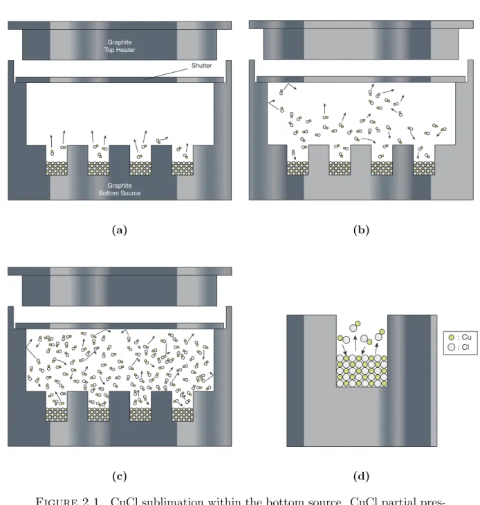
Figures 2.1a - 2.1d provide schematics of CuCl sublimation within the CSS chamber as the CuCl partial pressure increases to saturation within the source pocket geometry at a given source temperature Tsource. Sublimation begins with a few CuCl molecules having
enough thermal energy to break their solids bonds to become vapor (Figure 2.1a). Over time, a CuCl partial pressure continues to build within the pocket since the evaporation rate is greater than the condensation rate at the solid-gas interface (Figure 2.1b). At saturation (Figure 2.1c), equilibrium vapor pressure of CuCl is achieved since the evaporation rate is now equal to the condensation rate (Figure 2.1d). Therefore no further sublimation occurs in the pocket [17]. Once the substrate enters the source domain at temperature Tsubstrate
< Tsource, deposition will occur due to the CuCl gas molecules directly adjacent to the the
Graphite Bottom Source Graphite Top Heater Shutter (a) (b) (c) : Cu : Cl (d)
Figure 2.1. CuCl sublimation within the bottom source. CuCl partial pres-sure eventually reaches saturation as long as the surface temperatures within the pocket are equal and no leaks are present while the shutter is covering the source pocket. (d) is a zoomed representation of one of the bottom source wells from (c) when the evaporation rate is equal to the condensation rate at the solid-vapor interface.
equilibrium and thus sublimation is driven until the source sublimation rate, along with the deposition rate on the surface, again reaches equilibrium vapor pressure.
2.1.2. ADSORPTION. When the shutter is removed and the end-effector along with a substrate slides over the CuCl pocket, a thermal gradient is formed throughout the gaseous species (Figure 2.2). This is due to the substrate temperature Tsubstrate being less than the
temperature of the CuCl gas species monolayer directly adjacent to the substrate. The colder substrate surface acts as a thermal energy sink for these CuCl gas molecules, causing them to preferentially move toward it. As the CuCl vapor impinges on the surface, the gas molecule may lose enough kinetic energy during collision with the substrate in order to adhere to it, resulting in a process known as adsorption. Adsorption can either be a physical process that relies on Van Der Waals forces to hold the adsorbate gas species to the adsorbent bulk layer (a.k.a. physisorption) or a chemically activated process that combines both species with strong chemical bonds (a.k.a. chemisorption). The latter case creates a much stronger force and thus requires more energy to cause the gas molecule to desorb from the bulk layer. However, in this study physisorption is the dominant adsorption mechanism for CuCl on the FTO-coated substrate.
In order to fully understand how the adsorption rate is calculated, the rate of impingement by a gas on a particular surface must be determined. According to kinetic theory, the impingement rate is the amount of incoming molecules per second that hit a surface within a given area [18] and is expressed as follows:
(2.3) Φ = p P
2⇡M RT
where P = partial pressure of gas species impinging on the surface, M = gas species molar mass [kg/kg-mol], and T = temperature of the gas [K]. However, ANSYS!R
FLUENT tends to reformulate the impingement rate in terms of species concentration as oppose to
: Cu
Graphite Bottom Source (Tsource)
Graphite Top Heater
: Cl Substrate (Tsubstrate)
Tsubstrate < Tsource
Figure 2.2. CuCl adsorption occurring at the substrate. Adsorption is dic-tated by a sticking coefficient on a given surface that can be attributed to one of the three systematic growth mechanisms.
partial pressure. Therefore equation 2.3 can be rewritten as:
(2.4) Φ = CCuClg
r RT 2⇡M
where CCuClg is the CuCl molar concentration [kmol/m
3]. The impingement rate can be
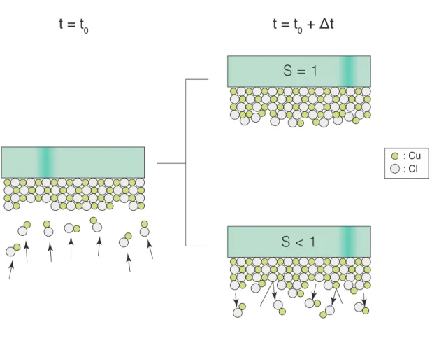
thought of as all incoming vapor molecules sticking to a surface. In reality, adsorption rates are typically much less than Φ due to imperfect surface conditions, preferred orientation, surface temperature, and ambient pressures. An overall representation of these complex limiting factors is known as the sticking coefficient S. This accommodating factor in its simplest form is written as:
(2.5) S = Radsorption
As depicted in Figure 2.3, an impingement flux of CuCl gas occurs at some initial time t0, after which some ∆t time passes, two possibilities are given: 1) all molecules impinging
on the substrate stick to it (S = 1), or 2) some molecules do not stick and are reflected back into the vapor species (S < 1). In most real-world cases, S is a value between 0 and 1. Since the sticking coefficient is associated with many varying conditions of a given system, it is difficult to obtain a general solution for S that encompasses a wide range of systematic processes. Nonetheless, its contribution to the adsorption rate is a key aspect in thin-film growth analysis. Within this research work the sticking coefficient is attempted to be generalized for a certain CuCl temperature regime and process condition. Calculating S as a function of temperature may lead to a quantifiable model of the CuCl adsorption rate, but a brief look at the types of possible growth mechanisms in thin-films will help assess what type of growth behavior CuCl exhibits.
2.1.3. GROWTH MECHANISMS. Three growth mechanisms are used to classify the growth behaviors of thin-films according to the type of substrate and overlayer used during deposition: i) Weber, ii) Frank-Van der Merwe, and iii) Stranski-Krastanov. Volmer-Weber growth occurs when clusters of the condensed species form islands on the substrate rather than a uniform layer. This is primarily due to the condensed species having a higher surface energy than the substrate to which it is adhering, making it more energetically favorable for island formation to occur. On the other hand, Frank-Van der Merwe is a layer-by-layer deposition phenomena in which the surface energy of the substrate is greater than the energy required to cluster the atoms together. The final mode known as Stranski-Krastanov growth is a combination of layered growth for the first few monolayers upon reaching a critical thickness where island growth becomes more favorable [18]. Previous studies have shown that the Stranski-Krastanov mode is prominent during CuCl heteroepitaxial growth on MgO
: Cu : Cl
t = t
0t = t
0+ Δt
S = 1
S < 1
Figure 2.3. Schematic demonstrating the significance of the CuCl sticking coefficient
substrates [19, 20]. It was not known if CuCl would display similiar growth characteristics within CSS as these studies, which is why the CuCl growth mechanism was investigated. Figure 2.4 illustrates the growth modes in various thin-film structures.
2.2. SPECIES MODELING THEORY ANSYS!R
FLUENT was the solver platform tool used for modeling the vaporization characteristics of CuCl during CSS. This engineering simulation program is geared toward computational fluid dynamics (CFD) as well as heat transfer/thermal modeling aspects. More specifically, FLUENT is capable of simulating finite-rate species transport and is most
Volmer-Weber Frank Van der Merwe Stranski-Krastanov t0 t0 + ∆ t t0 + 2 ∆ t
Figure 2.4. Primary growth modes displayed by various thin-films. Such modes are dependent on the surface energies of the substrate and adsorbed overlayer
applicable to this research work. For all simulations the species transport algorithm was en-abled for describing the CuCl volumetric and wall-adhering species governed by the following equation:
(2.6) @(⇢Yi)
@t + r · (⇢~uYi) = −r · (~Ji) + Ri+ Si
where ⇢ = density, ~u = momentum vector, Yi = local mass fraction, ~Ji = diffusion flux,
Ri = net rate production, and Si = source term of species i [21]. The first term on the
left-hand side of the equation is the rate of change of the species mass fraction while the second term is related to convection. On the right-hand side, the first term is the divergence of the diffusion flux, the second term is the rate of production of the gas species i, and the third term an additional species source expression. Since the CuCl simulation was defined to be a steady-state problem with negligible convection effects and no additional source terms,
FLUENT only needs to calculate the diffusion flux ~Ji as well as the net rate production
of species i. An important flow characteristic that affects how the divergence terms are calculated is known as the Knudsen number (Kn). This dimensionless value classifies the flow regime of species within the volume geometry based off of their mean free paths. In other words, Kn determines whether molecules interact with each other more or less often than the dimensional limits of the chamber that surrounds them. The typical expression for Kn is in the form of a ratio:
(2.7) Kn = λ
Lc
where λ is the mean free path of the gas molecule and Lc is the characteristic length
of the chamber. At low Kn < 0.1, a continuous flow regime due to the high number of gas-to-gas collisions ensures the validity of the Navier-Stokes equations. On the other hand, high Kn values > 10 are seen in the molecular flow regime where bulk properties of diffusion are no longer relevant [22]. In between such limits is the transition flow regime where the no slip condition on the wall boundaries is invalid and should be accommodated by enabling the low-pressure boundary slip condition in FLUENT. For this particular simulation, negligible change in the deposition rate is seen using this condition. Furthermore, previous research on the CdS/CdTe domains in the main deposition chamber revealed that Kn was not high enough to affect the Navier-Stokes equations [6]. Thus it is assumed to cause minimal effects to the fidelity of the CuCl simulation. In the laminar flow case, the diffusion flux can be described by:
(2.8) J~i = −⇢Di,mrYi− DT,irT
where Di,m= mass diffusion coefficient and DT,i = thermal diffusion coefficient for species
i. It is evident from equation 2.8 that the diffusion flux is dictated by both the concentration and thermal gradient across the CuCl vapor species and will consequently determine the deposition rate possible on a specified wall surface. Both the mass and thermal diffusion coefficients Di,m and DT,i were calculated using the available kinetic theory option under
mixture materials. Two inputs known as the Lennard-Jones (L-J) parameters were necessary for solving any material properties governed by kinetic theory. The L-J characteristic length σ is described as the equilibrium distance between two given atoms during which zero net energy (i.e. repulsive energy - attractive energy = 0) is acting on them. The energy parameter ✏/kb is attributed to the minimum potential energy well (i.e. highest attractive energy)
between two atoms that induce dipole moments in each other [23]. There are no readily available L-J parameters for CuCl within research literature, thus a simple calculation using data obtained from Monte Carlo simulations on Cu [24] and Cl [25] was performed via the Berthelot Mixing Rule:
σab = σaa+ σbb 2 (2.9) ✏ab =p✏aa✏bb (2.10)
where a and b refer to Cu and Cl, respectively. The calculated parameters for CuCl were σ = 2.789 ˚A and ✏ = 914.087 K.
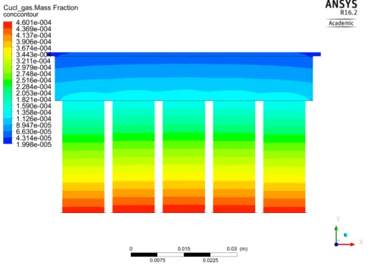
The Pressure-Based Coupled Solver used in this simulation initially solves for the mass and momentum equations, which is followed by the energy equation for each iteration. Such equations will compute the main domain properties such as temperature, density, enthalpy, velocity components, and pressure at each cell-center of the mesh. Thereafter equation 2.6
is calculated along with the aforementioned properties per iteration until their residuals con-verge to a steady-state condition. The final solution provides Yi cell-center values necessary
to describe the CuCl concentration gradient throughout the pocket (Figures 2.5a and 2.5b). The wall surface conversion process represented as CuCl species in the model is defined as:
b1
0
· CuClb + s1
0
· CuCls = s1”· CuCls+ g1”· CuClg
(2.11)
g2
0
· CuClg + s2
0
· CuCls = s2”· CuCls+ b2”· CuClb
(2.12)
where the g, s, and b subscripts respectively denote gas, site, and bulk species of CuCl. b1 0 , s1 0 , g2 0 , and s2 0
are the initial species stoichiometric coefficients while s1”, g1”, s2”, and
b2” are the final species stoichiometric coefficients of the kinetic processes. The subscripts 1
and 2 denote sublimation and impingement, respectively, and all stoichiometric coefficients are equal to 1. Since CuClg is assumed to be a non-dissociative molecule during the entire
simulation process, the equations are straightforward for converting species in both kinetic processes. Equation 2.11 states that the CuCl bulk species in combination with an available CuCl site will desorb from a wall surface in the form of a CuCl gas molecule at some rate constant kr. Similarly, equation 2.12 describes the wall surface kinetic rate for impingement,
during which the gas species CuClg cell-center values directly adjacent to the substrate wall
are converted into the CuClb bulk species values that are representative of the impingement
rate on the substrate (Figure 2.6). FLUENT interprets the process rate constants using the following Arrhenius expression:
(2.13) kr = Ar· Tβ· exp✓ −E
RT ◆
= Wall Boundary Face-Center = Gas Species Cell-Center (Unsolved) = Impingement Face-Center
= Gas Species Cell-Center (Solved) = Sublimation Face-Center
(a)
(b)
Figure 2.5. Schematic of species transport calculation throughout entire mesh domain. (a) Sublimation kinetic rate is enabled to allow FLUENT to compute and store the mass fraction Y for CuCl in the cell-centers that are compared to surrounding values that determine whether a solution for r~Ji = Ri has converged. (c) After convergence, the 1st adjacent cell-center
layer to the substrate impingement face-centers will influence the impingement rate calculated to obtain a simulated CuCl thickness.
It should be evident that equation 2.13 is a modified form of equation 2.2 with an ad-ditional temperature term raised to some β constant. Furthermore, the kr rate constant
Figure 2.6. Example of CuCl mass fraction calculated in simulation model based off of R1 (sublimation) at the bottom source and R2 (impingement) at
the substrate
sublimation and r = 2 for impingement, the final kinetic rates R1 and R2 may be expressed
as follows: R1 = −A1· exp ✓ −E RTsource ◆ + B1· CCuClg − C1 (2.14) R2 = A2· CCuClgpTsubstrate (2.15)
where A1 and A2 can be derived from calculating the constant terms in equations 2.2
and 2.4 respectively. B1 and C1 were included in equation 2.2 to provide additional
function-ality to the sublimation rate with respect to CuCl partial pressure if necessary. By activating these kinetic mechanisms on particular wall surfaces as well as applying the stoichiometric coefficients from equations 2.11 and 2.12, a net molar rate of production or consumption [kg-mol/m2-s] on a particular wall of the mesh domain can be calculated to determine the
gas, site, and bulk CuCl species. Equations 2.16 - 2.18 define these calculations for each respective term: ˆ Rg = ⇣ g1”− g1 0⌘ · R1 (2.16) ˆ Rs = 0 (2.17) ˆ Rb = ⇣ b2”− b2 0⌘ · R2 (2.18)
where g1” and b1” = 1 and g1
0
and b1
0
= 0. It should be noted that Rs = 0 means that
the CuCl site species is constant throughout the entire wall surface adsorption process. A reaction-diffusion balance is made at the wall during each iteration until steady-state con-vergence is achieved, during which the mass deposition rate on the wall surface is calculated:
(2.19) m˙dep = M · ˆRb
Again, M = CuCl molar mass [kg/kg-mol]. Converting the units of ˙mdep from [kg/m2-s]
to [nm/s] will ultimately lead to the simulated impingement rate Φ as shown by equation 2.20:
(2.20) Φ = m˙dep· 10
9
⇢
Multiplying the impingement rate Φ by the deposition time t provided a simulation thickness at each particular substrate and source temperature for further comparison to experimental thicknesses, which will be described in the next chapter.
CHAPTER 3
EXPERIMENTAL/SIMULATION METHODS
The experiments performed within this research were focused on quantifying both the sublimation and adsorption rates of CuCl during the CSS process. Since the simulation of CuCl thin-film growth rates required an accurate representation of sublimation within the CSS apparatus, CuCl mass-loss measurements were recorded and used for further sublimation rate calculations. This chapter will explain the method of measuring the CuCl sublimation rate and the obtained Arrhenius rate expression used within ANSYS!R
FLUENT. It will also elaborate on the multi-step technique developed to measure the CuCl thickness across the substrate at pre-determined locations. Finally a description of the mesh model, along with its boundary conditions obtained from theoretical aspects defined in Chapter 2, will be elaborated for CuCl thickness simulations. This chapter aims to bridge the gap between CuCl experimental and simulated growth rate results.
3.1. CSS TECHNIQUE IN CuCl THIN-FILM GROWTH
CuCl growth rates were varied by sweeping a range of thermal parameters for each deposition run using the Advanced Research Deposition System (ARDS). This versatile tool contains several CSS stations, each equipped with a graphite top heater and bottom heating source where the material powder, in this case CuCl, is sublimated. Both the top heater and bottom source temperatures are adjusted by electrically heating the Nickel-Chromium coil embedded in each graphite fixture and maintained via PID control. The heaters were kept at near steady-state conditions since temperature fluctuations (top heater: 1-2◦C, bottom
source: < 1◦C) occurred due to the PID control setup. Approximately 63.9 SCCM of mixed
of 40 mTorr using a Leybold D65 rotary vane mechanical pump and a Varian VHS-4 diffusion pump.
Pilkington TEC-12D glass substrates (78 x 90 mm2) were used during each deposition
run and were ordered with a TCO pre-layer consisting of FTO covering one side of the glass. The substrates were initially rinsed, sonicated, and N2 dried [11] to keep surface conditions
as clean as possible. All substrates were plasma-cleaned in a 200 mTorr N2 environment for
30 s before entering the main chamber. Initial CuCl experiments were performed at normal process of recipe (POR) conditions, which pertain to heating the substrate to > 400◦C prior
to thin-film deposition and depositing CuCl on the substrate for 110 s. However, thicknesses of the resulting CuCl thin-films were too inconsistent to be measured with any available instruments. Therefore, it was decided that all substrates were to directly enter the CuCl domain without pre-heating and deposit for one hour to obtain easily measurable CuCl thin-films as well as reach steady-state equilibrium conditions within the domain. As a result, CuCl films were produced with a thickness that could be measured consistently and accurately.
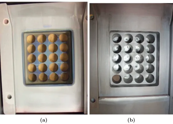
Two sets of experiments were ran in the ARDS: 1) full-well and 2) single-well deposition. Full-well deposition refers to all 20 wells in the graphite bottom source being 1/2 filled with CuCl powder, which is the typical POR setup for all sublimation sources. As the name implies, single-well deposition only used one well 1/2 filled with CuCl while leaving the other 19 source wells empty. Simulation models for both cases were also developed and compared to the experiments. The full-well deposition case was used to check the initial accuracy of the impingement rate obtained from the simulation and compare it to the actual adsorption rate given by experimental data. A sticking coefficient curve fit for each substrate and source temperature could then be obtained for later use with the single-well deposition model. The
full-well runs were also used to determine the growth mode exhibited by CuCl on the FTO layer via characterization analysis. The main goal for using the single-well deposition case was to verify the model’s accuracy in describing the physical processes associated with CSS during an extreme processing condition. Actual images of the full and single-well CuCl setups can be found in Figures 3.1a and 3.1b.
(a) (b)
Figure 3.1. (a) Full-well and (b) single-well depositions in the ARDS. Upon further analysis, the distinct color difference between experiments indicated whether the CuCl powder continuously sublimated (darker) or not (lighter) after completing all deposition runs.
Top heater and bottom source temperatures were systematically varied per substrate. It was necessary to determine the substrate temperature during each deposition run. However the Mikron-MI-N5/5+ series pyrometer installed at the CuCl chamber entry was unable to properly measure the substrate temperatures, either due to calibration error in emissivity, pyrometer positioning, or a combination of both. It was decided that substrate temperatures were to be calculated using a simplified radiation heat transfer expression dependent on the
top and bottom CuCl coil temperatures. The net radiation between two surfaces [26] is found by: (3.1) q12 = σ(T14− T24) 1−✏1 ✏1A1 + 1 A1F12 + 1−✏2 ✏2A2
where σ = Stefan-Boltzmann constant [5.67 ⇥ 10−8 W/m2·K4], F
12 = view factor, ✏1,
✏2 = emissivity, A1, A2 = surface area, and T1, T2 = surface temperatures for surface 1
and 2, respectively. The following assumptions were made during the substrate temperature calculation:
(1) Substrate glass emissivity is constant on the top surface (✏s,t = 0.8)
(2) TCO emissivity on the bottom of the substrate is constant (✏s,b= 0.2)
(3) Top heater, bottom source, and substrate surfaces considered to be parallel long plates since they are all in close enough proximity to each other
(4) All surfaces are isothermal
(5) Steady-state conditions have been reached
Such assumptions were reasonable considering the graphite heaters were uniform in tem-perature (±1◦C) and the deposition time (1 hr) was longer than necessary to reach
steady-state thermal conditions in the CuCl domain. Figure 3.2 illustrates the concept of the substrate temperature calculation. Using these assumptions and solving the energy balance by equaling the radiation heat transfer rates between the bottom source to the substrate (qbottom−substrate) and substrate to the top heater (qsubstrate−top), the substrate temperature
was expressed as:
qsubstrate-top
Tsubstrate TCuCl, top < Tsubstrate < TCuCl, bottom
TCuCl, top
TCuCl, bottom εs,t = 0.8
εs,b = 0.2
qbottom-substrate
Figure 3.2. Illustration of the substrate temperature calculation
where TCuCl,bottom and TCuCl,top were the respective bottom and top CuCl heater
temper-atures. All substrate depositions (full and single-well) were classified by their substrate and source temperatures as recorded in Tables 4.1 and 4.4 found in Chapter 4.
3.2. CuCl MASS-LOSS EXPERIMENT
Studies on CuCl vapor pressure [7, 27–29] during sublimation were analyzed to see if their vapor pressure curves embodied the standard kinetic rates found in the ARDS operation regime. However, CuCl sublimation rates at temperatures < 300◦C were not well defined in
previous literature and most studies performed experiments at different baseline pressures than the typical ARDS operating pressure (40 mTorr). Larger molecular vapor species such as Cu3Cl3 trimers are more prevalent at higher temperatures than the expected CuCl vapor
[7], further deviating from CSS conditions. It was not known if such sublimation rates were representative of that seen in CSS and was therefore imperative to obtain an empirical expression for the CuCl sublimation rate within the ARDS. This would ensure the data
used to calculate the sublimation rate were within the applicable temperature and pressure regimes and could be applied to the simulation model.
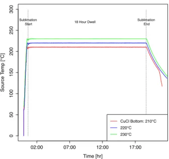
The CuCl mass-loss experiment was performed in the ARDS CuCl bottom source using four graphite crucibles machined to fit in the source wells. Each crucible was weighed five times before and after sublimating using a Mettler AE163 mass balance. The crucibles were filled with 1/4 tsp of CuCl powder and baked for approximately 18 hours to minimize the amount of water vapor accumulation in the materials and replicate typical CuCl powder conditions after an extended period of usage. The crucibles were sublimated at 210, 220, and 230◦C for 18 hours at each temperature to ensure steady-state sublimation. Previous
experiments revealed prolonged exposure to ambient conditions noticeably affected mass measurements. It is believed that water vapor was the main culprit to this detrimental factor. Each experiment run was performed immediately after measuring CuCl mass to prevent the crucibles and/or CuCl powder from collecting water vapor and resulting in misleading mass analyses. Temperature logs were recorded for the bottom source within the CuCl domain to determine whether thermal equilibrium was sustained throughout the entire sublimation process (Figure 3.3). After calculating the CuCl mass-loss at each particular source temperature and crucible, a log curve fit was applied to the entire data set to define the sublimation rate as an Antoine expression shown in equation 2.1:
(3.3) log(Rsublimation) = −6503.8
T + 4.8741
The Arrhenius rate expression derived from equation 3.3 is provided:
(3.4) Rsublimation = 74831.93 · exp
✓ -1.2451e8 RT
◆
02:00 07:00 12:00 17:00 0 50 100 150 200 250 300 Time [hr] Source T emp [°C] CuCl Bottom: 210°C 220°C 230°C 18 Hour Dwell Sublimation
End Sublimation
Start
Figure 3.3. Temperature plot of the 18-hr sublimation experiments ran at CuCl bottom source temperature = 210, 220, and 230◦C
As previously mentioned in Chapter 2, the temperature-dependent Arrhenius rate ex-pression was applied to the simulation model as the driving mechanism for sublimation in the CuCl source pocket. This would allow for the CuCl concentration to be calculated throughout the CuCl pocket domain and influence the impingement rate on the substrate. The fulfillment of the CuCl mass-loss experiment provided empirical data for the CuCl sub-limation rate within the CSS system operating at 40 mTorr and was implemented in the CuCl growth simulation model for further thin-film growth analysis.
3.3. CuCl THICKNESS MEASUREMENT TECHNIQUE
3.3.1. FORMER METHODS. A consistent method needed to be developed in order to compare experimental growth processes to simulated behaviors. However, many challenges were encountered in measuring CuCl thin-film thickness due to short deposition times and measurement techniques. In previous research of Cadmium Sulfide deposition within the ARDS [6], the primary method of measuring the thin-film thickness was to mask one side
of the diagonal of the substrate with etchant tape and etch away the unmasked side with Hydrochloric Acid (HCl). Doing so created a step height between the now bare TCO layer and the CdS overlayer that was measured across the entire substrate diagonal. Similar attempts were made to measure the CuCl thicknesses using this method while depositing CuCl near POR conditions (110 s). But since CuCl was much thinner than CdS at POR, etching one side of the CuCl layer would unexpectedly roughen the TCO below and lead to misleading thickness results.
The next attempt included dripping one or a combination of the three solutions, Iso-propanol (IPA), de-ionized water (DI), or Acetone, on the CuCl layer to create craters as the measured step heights. CuCl deposition was again done for 110 seconds. Unfortunately the craters formed by either solution migrated CuCl to their outer perimeters and caused erroneous delta steps that were not representative of the thickness as shown in Figures 3.4a and 3.4b. The same effect occurred when substrates were dipped in either IPA or DI. Fur-thermore, the 110 s CuCl depositions had very little CuCl on the substrates (< 5 nm), making measurements unfeasible with the available instruments.
3.3.2. CURRENT METHOD. A new multi-step method was implemented to measure the CuCl thicknesses accurately and consistently. The method is summarized into three sub-sequent steps: 1) Argon Ion Beam sputtering to form a crater deep enough into both the CuCl and TCO layers, 2) measuring the crater depth using scanning white light interferom-etry (SWLI), and 3) etching CuCl overlayer with HCl and remeasuring the crater depth to determine the overall step height difference.
3.3.2.1. Argon Ion Beam Sputtering. The Argon Ion Beam in the X-ray Photoelectron Spectroscopy (XPS) instrument was utilized to create 10 craters shaped like a rounded rectangle across the diagonal of each substrate. Micrometer dial positions were determined
(a)
(b)
Figure 3.4. (a) Contour representation and (b) thickness profile plot of CuCl after DI and Acetone was dripped on substrate. Generalizations of CuCl thin-film growth with respect to temperature could not be made using this inconsistent method, thus a new technique was devised for measuring CuCl thicknesses.
for each particular crater location to ensure coordinate consistency (Figures 3.5a, 3.5b). As shown in Figure 3.6, the Ion Gun propelled ionized Ar atoms toward the substrate with an accelerating voltage of 5 kV, using kinetic energy to collide with the exposed surface atoms and remove them. Over time a crater would develop within both the CuCl and TCO layer below so that a thickness step height could later be measured. Typical operating pressures within the XPS were 9⇥10−8−2⇥10−7 Torr over the duration of the Ar+sputtering process. Each process was timed for 5 minutes to form a crater deep enough in the CuCl and TCO layers1.
(a) (b)
Figure 3.5. (a) Expected CuCl crater locations and (b) typical crater loca-tions on a TEC-12D substrate. The substrate is divided into 3 x 3 samples that are labeled by position values 1-9. Only positions 3, 5, and 7 are used for crater etching Argon Ion Beam CuCl TEC-12D Glass TCO
Figure 3.6. Schematic of CuCl/TCO crater formation during Ar+sputtering
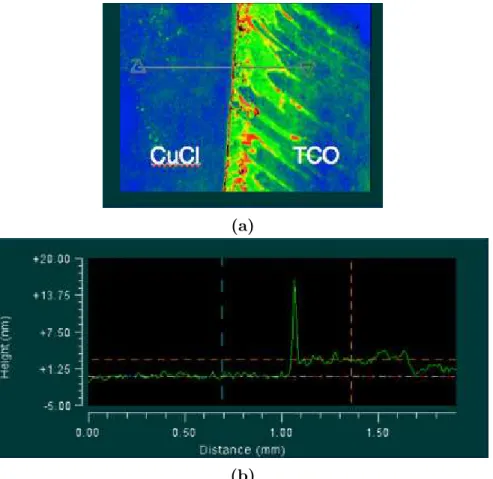
3.3.2.2. Scanning White Light Interferometry. The NewView 7300 instrument used for measuring the CuCl thicknesses is known as a Scanning White Light Interferometer (SWLI). This tool implements a nondestructive technique known as Coherence Scanning Interferom-etry [30] that evaluates the metrology of a sample using a broadband spectrum (white light) traveling toward the surface and reflects off of it, producing interference fringes at a cer-tain scan height. The instrument vertically scans the entire topology along its optical axis, obtaining contrast fringes throughout the entire scanning process. Frames at each height variation are acquired successively by a 640⇥480 pixel CCD camera and processed into an areal (3-D) representation of the surface (Figure 3.7a). For each small sample (26 x 30 mm2)
SWLI measured the crater depth before etching the CuCl thin-film with HCl. After the first measurement, the CuCl layer was removed with HCl and cleaned with DI and IPA to eliminate etchant residue and marks. A second measurement was performed on the etched samples to determine the remaining TCO crater depth. The difference between the first and second depth measurements resulted in a CuCl thickness at the crater location.
For all measurements, a gaussian spline low-pass filter with a filter high wavelength of 0.08 mm was included to reduce the surface noise due to CuCl roughness (3-5 nm) and establish a CuCl thickness measurement closer to the average step height difference. The instrument scanning distance was set at 40 µm to capture the entire topology on the substrate surface. As shown in Figure 3.7b, a reference and test mask were created as the crater depth displacement planes and all measurements were recorded using the evaluated peak-to-valley mean values. For the reference mask areas (longer rectangular areas), a best fit cylinder form was applied to remove the curvature within each sample due to thermal warping while in the ARDS chamber. As a result, the mean top plane was analyzed in place of the curved surface plane. Within the test mask (large square area) a high clipping parameter was specified to
(a) Reference Mask Test Mask
Reference
Test
(b)Figure 3.7. (a) Areal representation of a typical CuCl crater measured with SWLI. (b) Test and reference mask used within CuCl crater depth analysis, where the test mask is the entire area shaded in orange (purple) and the reference masks are the long rectangular boxes used as leveling planes for each data set.
remove any data > 2 nm above the deepest part of the crater. The average of the remaining several thousand data points within the deepest crater area was used to measure the mean CuCl step height to the top reference plane. The measurement process at each crater location was repeated across the substrate diagonal and compared to the CuCl thickness simulation results.
3.4. SIMULATION METHOD
The CuCl thin-film growth simulation model required an extensive study on material properties of CuCl from various literature sources [31–35] as well as experimental data ob-tained from this study. A CuCl materials database, along with any materials used within the ARDS, were compiled in order to properly develop the thermal and diffusional charac-teristics of CuCl amidst a N2-O2 bulk gas in the pocket mesh. As shown in Figure 3.8a and
3.8b, the 3D CuCl mesh model used during the CuCl growth rate simulation consisted of 45772 nodes with a minimum orthogonal quality of 0.49 and maximum skewness of 0.74.
These mesh property values were considered to be adequate for computationally accurate simulations of CSS. Only steady-state simulation analyses were conducted in this research study since the one hour deposition time used in the experiments was assumed to achieve steady-state thermal and kinetic conditions within the ARDS. Furthermore, using transient analysis did not improve the modeling accuracy and thus only extended the computational time necessary to reach convergence.
Certain mesh boundaries were specified as primary sublimation or impingement surfaces. The largest volume of the mesh geometry represented the CuCl bottom source pocket where the cylindrical wells contained the CuCl powder to be sublimated into a vapor species. The top mesh region composed of the smaller volume region encased by the end effector walls and the substrate surface adjacent to the pocket domain. Depending on whether a full-well or single-full-well simulation was performed, the bottom full-well sources were marked as walls separate from the other pocket geometry boundaries and assigned as sublimation sources defined by equation 3.4. The substrate face was classified as the impinged region with a rate described by equation 2.4 (Figure 3.8c). The inputs for each simulated case were the source and substrate temperature along with their respective kinetic mechanism (see Section 2.2 for more information on the species modeling theory). The entire bottom source wall boundaries were kept at a uniform temperature since thermocouple data showed only a ±1◦C difference
between the bottom source side walls (see Appendix B for more information).
CuCl sublimation and impingement was enabled after initializing and converging the ini-tial state inputs with regards to temperature on each wall (1000 iterations). Each simulation was ran until the residuals reached suitable convergence (approximately 3000 iterations per case). Using 150 points plotted across the substrate wall diagonal (Figure 3.9), the CuCl deposition rate was obtained at each point. The data was exported with columns of the
Substrate
CuCl
Source
Figure 3.8. CuCl (a) mesh model used during FLUENT simulation, and (b) contour example when kinetic rates were activated to determine the CuCl mass fraction throughout the pocket. This example was performed at a sub-strate and source temperature of 180.6◦C and 210◦C, respectively. (c)
Speci-fied kinetic rates R1 and R2 at the bottom well source and top substrate wall
boundaries, respectively.
deposition rate [nm/s] and location along the substrate diagonal [mm]. All deposition rates were multiplied by t = 3600 s to determine what the predicted thickness would be after one hour deposition and were compared to experimental results according to substrate and source temperature parameters.
Figure 3.9. Examples of full well and single well simulation deposition rates. Along the black dotted line are where 150 points were mapped across the sub-strate diagonal to measure the deposition rate profile from position 3 to 7 (referenced by Figure 3.5a) on the substrate for comparison to experimental results. These two examples were modeled at a substrate and source temper-ature of 191.7◦C and 210◦C, respectively.
CHAPTER 4
RESULTS/DISCUSSION
CuCl thicknesses were obtained for full-well CSS depositions as a function of substrate and source temperatures. Sticking coefficient values were calculated and plotted to develop curve fitting parameters that would improve the initial accuracy of the full-well simulation models. The converged model along with sticking coefficient curves for a given source tem-perature was later applied to single-well depositions to verify its computational accuracy at such a vastly different process condition. In order to gain a further understanding of the inherent growth mechanisms exhibited by CuCl during CSS process conditions, characteriza-tion via Scanning Electron Microscopy (SEM) and Electron Dispersion Spectroscopy (EDS) were performed on the full-well experiments. This chapter aims to provide the aforemen-tioned results while elaborating on their significance to CuCl thin-film deposition and growth analysis. A discussion on the various implications within the data will be made, which will be used to draw conclusions on the proposed CuCl growth mode as well as current modeling accuracy in representing the CuCl vaporization process and the resulting thin-film uniformity during CSS.
4.1. FULL-WELL DEPOSITION
As mentioned in Section 3.1, TEC-12D substrates initially entered the ARDS chamber without prior heating, during which CuCl was deposited for one hour. Substrates with a lower surface temperature during CSS deposition were visibly covered with a white-colored film on the TCO layer, which became more transparent as the temperature increased. All full-well depositions along with their average top heater, bottom source, and calculated substrate temperatures are listed in Table 4.1.
Table 4.1. Full-well CuCl CSS deposition runs in the ARDS
Bottom Source [◦C] Top Heater [◦C] Calculated Substrate [◦C] Sticking Coefficient S
210.0 171.0 180.6 0.9381 210.1 180.6 187.9 0.9623 210.1 186.0 191.7 0.8493 210.0 191.0 195.4 0.5598 210.0 210.9 210.7 1 0.0067 199.9 171.0 177.9 0.5929 200.1 175.1 181.0 0.5016 200.1 180.8 185.3 0.3645 190.1 166.5 172.1 0.3230 190.1 170.8 175.3 0.2486 190.1 176.2 179.4 0.2013
As explained in Section 3.4, 150 points were used to measure the CuCl impingement rate across the substrate wall boundary. The average impingement rate across position 5 (see Figure 3.5a) of the virtual substrate was determined for all simulations. It was noticed that there was minimal change to the value as the substrate temperature increased, therefore the impingement rates shown in Table 4.2 were those typically computed with respect to a given source temperature.
Table 4.2. Simulated CuCl impingment rate Φ [nm/s] at each source temperature Bottom Source [◦C] Φ [nm/s]
210 0.0347
200 0.0182
190 0.0093
CuCl simulated thicknesses observed from these impingement rates had larger magnitudes in comparison to the experimental values. This is due to the sticking coefficient on the substrate being less than unity, meaning that not all CuCl vapor molecules impinging on the surface adsorb to it. Therefore by dividing all experimental adsorption rates by the simulated impingement rates at a given bottom source temperature, a sticking coefficient as
1Experiment used to verify that no deposition would occur when all temperatures were approximately the same
a function of temperature was recorded in order to systematically converge the simulation model to the experimental results. Several logistic curve fits were computed using sticking coefficients found at each full-well deposition run (see Table 4.1). Equation 4.1 denotes the logistic S curve fit found for each source temperature:
(4.1) S(T ) = 1
1 + ↵ · exp⇣R(Tsubstrateβ−Tsource) ⌘
where ↵ and β are fitted parameters and the temperature variables are in Kelvin. Ta-ble 4.3 refers to the parameter values based off of the source temperature. The sticking coefficient values were grouped in this manner for clarity of the relationship between ther-mal conditions of the substrate and bottom source and how each of them affects CuCl growth. Although a detailed physical explanation has not yet been discovered for each of the curves, the general concept is that ↵ loosely defines the mechanism by which molecules accumulate or get rid of excess energy [36] while β is more closely related to the activation energy of the adsorbed CuCl molecules to the TCO surface. Tsource in the denominator of the exponential
function is included so that an asymptotic cutoff can be establish when the substrate tem-perature is greater than the bottom source temtem-perature. In essence, no sticking will occur (S = 0) on the substrate when Tsubstrate > Tsource. The simulation accuracy was improved by
applying the S curve fits in Figure 4.1 to the original simulated thicknesses. From a general perspective, the S curve fit plot as well as impingement rates found in Table 4.2 are beneficial tools that can be used in future deposition runs to determine the adsorption rate of CuCl at some given CSS thermal condition. They eliminate the need for costly trial and error experiments to find a suitable CuCl average thickness. The method for calculating S can be extended to virtually any material as long as enough experimental values are recorded to establish the appropriate ↵ and β fitting parameters.
Table 4.3. S curve fitted parameters used for each source temperature Bottom Source [◦C] ↵ β 210 4.886e-4 895633.7 200 0.1143 334909.5 190 0.8913 136154.0 400 420 440 460 480 500 0.0 0.2 0.4 0.6 0.8 1.0 Substrate Temperature [K] S Source: 190°C Experiment Fit Source: 200°C Experiment Fit Source: 210°C Experiment Fit
Figure 4.1. S curve fits at each source temperature using equation 4.1.
All full-well deposition runs and simulated thicknesses are shown in Figures 4.2a - 4.2c2. It
is worth noting that the scales for each plot are not the same to avoid any confusion between some conclusions on particular data sets. Analyzing only the experimental results, several descriptive qualities appear within the CuCl thickness. It is apparent that the thermal gradient between the substrate and bottom source will contribute to how thick the CuCl thin-film layers will become. However, there is a limitation to its effect on the adsorption
2Any error bars presented for CuCl thickness are summarized as follows: Horizontal = measurement error from expected crater location; Vertical = interpolated thickness error determined by shift in crater location
0 20 40 60 80 100 120 0 50 100 150 Substrate Position [mm] CuCl Thickness [nm] 180.6°C Exp Sim 187.9°C Exp Sim 191.7°C Exp Sim 195.4°C Exp Sim 210.7°C Exp Sim (a) 0 20 40 60 80 100 120 0 10 20 30 40 50 60 70 Substrate Position [mm] CuCl Thickness [nm] 177.9°C Exp Sim 181.0°C Exp Sim 185.3°C Exp Sim (b) 0 20 40 60 80 100 120 0 5 10 15 20 Substrate Position [mm] CuCl Thickness [nm] 172.1°C Exp Sim 175.3°C Exp Sim 179.4°C Exp Sim (c)
Figure 4.2. Full-well deposition experimental and simulated thicknesses at a source temperature of (a) 210, (b) 200, and (c) 190◦C
rate dictated by the sticking coefficient. This means that once the sticking coefficient S reaches unity, the adsorption rate will remain constant regardless of how large the thermal gradient becomes when the source temperature is unchanged. A much more influential parameter according to these plots is the source temperature. The CuCl thin-films become
much thicker when the source temperature increases from 190◦C to 210◦C due to an increase
in the sublimation rate. Because of the larger sublimation rate, a higher CuCl vapor pressure would exist near the exposed substrate face that promotes more CuCl to adsorb on it. This is further validated by noticing that the gas species concentration in equation 2.4 is linearly dependent to the overall impingement rate while the substrate temperature only has a square root dependence. It is evident that the source temperature, and thus the amount of CuCl gas in the pocket, is one of the major driving forces to CuCl growth.
Another notable characteristic in the results is the slightly thicker CuCl film on the left side of several substrates (15-35 mm range on the substrate position, or Position 3). Thermocouples placed on the bottom source and shielding surrounding the side of the CSS domain revealed two things: 1) the CuCl bottom source had a temperature gradient of 1◦C
and thus was assumed to be thermally uniform, and 2) a significantly larger thermal gradient of 13-15◦C was measured from the right face to the left face of the shielding. This gradient
was due to the overall temperatures in the domains directly adjacent to the CuCl domain. On the side where the CuCl film appeared to be thicker, an “open” domain sat next to the CuCl domain and contained no thermal sources that drove it to a specified temperature. On the other side, however, the “anneal” domain used for Cu annealing was maintained at 200◦C during deposition. The thermal gradient across the side shielding was initially
thought to explain why the substrate position adjacent to the open domain was thicker than the position closer to the anneal domain. An attempt to validate this proposition was made by running a FLUENT thermal simulation with the thermocouple data3and emissivity
specified for the shielding and source materials [37–39]. Despite this obvious difference in shielding temperatures, the simulation showed no significant thermal non-uniformity on the

![Figure 1.2. Original and modified CdS source contour plots demonstrating the improved deposition rate uniformity across the substrate (image taken with permission from [6])](https://thumb-eu.123doks.com/thumbv2/5dokorg/5522650.144089/16.918.120.791.720.1003/original-modified-demonstrating-improved-deposition-uniformity-substrate-permission.webp)