UPTEC ES 18 027
Examensarbete 30 hp
Juni 2018
Characterization of combinatorial
Cu
2
ZnSnS
4
thin films
Joakim Adolfsson
Teknisk- naturvetenskaplig fakultet UTH-enheten Besöksadress: Ångströmlaboratoriet Lägerhyddsvägen 1 Hus 4, Plan 0 Postadress: Box 536 751 21 Uppsala Telefon: 018 – 471 30 03 Telefax: 018 – 471 30 00 Hemsida: http://www.teknat.uu.se/student
Abstract
Characterization of combinatorial
Cu
2ZnSnS
4thin films
Joakim AdolfssonThe kesterite Cu2ZnSnS4 (CZTS) is considered as a possible absorber layer in future
photovoltaic (PV) applications. The abundance of its constituent elements along with the material being non-toxic and having a direct band gap of around 1.5 eV make it an attractive material for solar cell applications. So far, cells with an efficiency of 12.6 % have been achieved. The limiting factor is the finished cells' open circuit voltage (VOC) deficit which has been attributed to structural defects in the material.
Problems with sustaining a sulfur-enriched atmosphere during the annealing step of material production have been observed, and are thought to be partially responsible for the high density of structural defects. Elemental sulfur is commonly used for inducing a sulfur-enriched atmosphere in the anneal. In this study, four combinatorial and polycrystalline CZTS thin films were prepared and annealed in different
conditions with regards to time, sulfur source and amount. The samples were characterized using Energy dispersive-, Raman- and Photoluminescence spectroscopy. The effect of the anneal on the different composition regions were analyzed and secondary phases were identified. Introducing CuS as the sulfur source during the anneal reduced the decomposition of the CZTS phase, and lowered the density of the defect complex [ZnCu + CuZn], while enlarging the single phase region. Strictly and
highly Sn-rich compositions of CZTS was observed to yield both high cation order and photoluminescence intensity, and a link between the two parameters was observed.
Ämnesgranskare: Charlotte Platzer-Björkman Handledare: Katharina Rudisch
Populärvetenskaplig Sammanfattning
Den växande populationen och den fortsatta utvecklingen av moderna teknologier för med sig en förväntan på ett ökat energibehov i världen. Organisationen Inter-national Energy agency (IEA) förutspår att det år 2050 kommer att konsumeras cirka 33,000 TWh per år, globalt sett (IEA 2018). Att denna energi skall pro-duceras som den gör idag är otänkbart då vi redan nu ser hur vår användning av fossila energikällor, med deras tillhörande utsläpp av växthusgaser påverkar vår miljö och omgivning. Därför är det av yttersta vikt att andra, miljövänliga och förnybara alternativ utvecklas och vinner mark inom området energigenerering. Att bemästra tämjandet av solens energi har länge varit lockande för människan. Startskotten skedde i och med den franska fysikern, Antoine-César Becquerels upp-täckt av den fotovoltaiska effekten år 1839 (PVEducation 2018). Därefter, år 1883 producerade Charles Fritts vad som anses vara den första solcellen (ibid.). De tidiga solcellerna hade dock verkningsgrader under 1% (ibid.). Idag finns solceller (single junction) som kan konvertera uppemot 28.8% av den infallande solenergin till elektricitet (NREL 2018). Dock finns det flaskhalsar i en framtida utbyggnad av dagens kommersiella teknologier. Framförallt är materialtillgången ett problem, inte just den totala mängden tillgänglig utan snarare brytningstakten och konkur-rensen med andra marknader (Schmalensee et al. 2015). Av denna anledning är
materialet Cu2ZnSnS4 (CZTS) en stark kandidat för ett framtida
solcellsmate-rial, ty materialet består av endast vanligt förekommande grundämnen och är ofarligt för miljö och människa. I dagsläget har forskare lyckats producera sol-celler baserade på CZTS med en verkningsgrad på 12,6%, vilket är långt under de kommersiella teknologierna. Den största anledningen för materialets, i jämförelse
låga verkningsgrad är dess låga öppenkretsspänning (VOC). Detta tycks bero på
rekombination av elektron-hål par i materialets bulk till följd av ett överflöd av strukturella defekter i kristallstrukturen.
För att kunna öka verkningsgraden hos CZTS-solceller behövs en utökad förståelse av sambandet mellan CZTS-fasens sammansättning och förekomsten av struk-turella defekter och sekundära faser. Vidare behöver strategier inom produktionen utvecklas för att till viss mån kontrollera dessa materialdefekter. Idag använder man sig av en två-stegs process, innefattande en deposition av materialets bygg-stenar på ett substrat, vanligen glas följt av en re-kristalliserings process (härd-ning). I härdningsprocessen har det visats att materialet förlorar en del av sitt tenn- och svavelinnehåll genom avdunstning vid normala härdningstemperaturer
på 400 − 600.◦C (Ren 2017). Detta leder till nedbrytning av CZTS fasen till
svaveltryck i härdningsprocessen. Genom att skapa en svavelberikad atmosfär i processen kan man reducera avdunstningen. Vidare innehåller det härdade mate-rialet ett överflöd av strukturella defekter. En defekt av särskilt intresse involverar ett platsbyte i kristallstrukturen mellan koppar och zink atomer. Defektens låga formationsenergi gör den vanligt förekommande i materialet. Inom forskningsom-rådet tror man att denna defekt är delvis ansvarig för den låga öppna kretsspän-ningen i solceller baserade på CZTS (Malerba et al. 2017)(Timmo et al. 2017). Defektens förekomst har visats kunna reduceras genom en låg-tempererad termisk behandling efter härdningsprocessen. Detta har visats i åtskilliga forskningsrap-porter, däribland Scragg et al. (2014).
Detta projekt ämnar undersöka samspelet mellan materialets sammansättning och härdningsprocessens utförande. Betydelsen för det färdiga materialets kvalité un-dersöktes, med avseende på strukturella defekter samt formation av sekundära faser. Genom att förstå samspelet bättre kan man identifiera en lämplig härd-ningsprocess för CZTS tunnfilmer i syfte att användas till solceller. Undersöknin-gen har gjorts Undersöknin-genom att förbereda fyra CZTS tunnfilmer av kombinatorisk och polykristallin karaktär, vilket innebär att sammansättningen av CZTS fasen vari-erar över filmens yta. Dessa har sedan härdats med olika utföranden. Tiden i pro-cessen har varierats, såväl som tillvägagångssättet för att skapa en svavelberikad atmosfär. Filmerna har sedan karakteriserats med optiska metoder, mer bestämt energidispersiv röntgenspektroskopi för att fastställa deras sammansättning och Raman-, samt fotoluminiscens-spektroskopi. De två sistnämnda syftar till att un-dersöka CZTS fasens kvalité, identifiera sekundära faser, kvantifiera förekomsten av koppar-zinkdefekten samt undersöka filmernas radiativa rekombination.
Executive Summary
In this study, four combinatorial and polycrystalline Cu2ZnSnS4 (CZTS) thin films
were prepared and annealed in different conditions regarding time, sulfur source and amount. The samples were characterized using energy dispersive-, Raman-and photoluminescence spectroscopy. The effect of the anneal on the different composition regions were analyzed and secondary phases were identified. Intro-ducing CuS as the sulfur source during the anneal reduced the decomposition of
the CZTS phase, and lowered the density of the defect complex [ZnCu + CuZn],
while enlarging the single phase region. The sufficient amount of CuS for 13 min anneals seem to lie in the range 11 − 31.6 mg, more investigation of the range is needed. Strictly and highly Sn-rich compositions of CZTS was observed to yield both high cation order and photoluminescence intensity, and a link between the two parameters was observed. Therefore, this study suggest that CZTS devices with a highly Sn-rich composition should be investigated. The observed photo-luminescence peaks’ asymmetric shape indicate that the samples produced still have a high density of structural defects and the dominating recombination route is concluded to not be band to band.
Contents
1 Introduction 1
1.1 Scope of the Project . . . 3
2 Theory 4 2.1 The Kesterite CZTS . . . 4
2.1.1 Material requirements and availability for multi-terawatt de-ployment of CZTS solar cells . . . 4
2.1.2 The CZTS material . . . 5
2.2 Secondary phase formation in CZTS . . . 7
2.3 Analysis techniques . . . 8
2.3.1 Energy dispersive x-ray spectroscopy . . . 9
2.3.2 Photon-Crystal lattice interaction, Raman and photoluminescence . . . 9
3 Method 13 3.1 Preparation of samples . . . 13
3.1.1 Precursor deposition . . . 13
3.1.2 High temperature anneal . . . 14
3.1.3 Post-anneal ordering treatment . . . 15
3.2 Characterization of samples . . . 15
3.2.1 Elemental analysis . . . 16
3.2.2 Raman and photoluminescence spectroscopy setup . . . 16
4.1 Compositional analysis . . . 20
4.2 Components of a CZTS Raman spectrum . . . 20
4.3 Secondary phase identification . . . 21
4.4 Distribution of secondary phases . . . 27
4.5 Identification of the single phase region . . . 30
4.5.1 Influence of annealing conditions/partial sulfur pressure on SPR and secondary phase formation . . . 32
4.6 Investigation of the CZTS cation disorder . . . 32
4.7 Photoluminescence of CZTS . . . 36
4.7.1 The effect of composition and annealing conditions on PL intensity . . . 37
4.7.2 The effect of composition and annealing conditions on PL peak position . . . 39
4.7.3 The photoluminescence’s dependence on cation order . . . . 41
1
Introduction
With the growing world population and the continuous development of modern technology, the demand for energy is expected to increase rapidly worldwide. In combination with the ongoing climate changes, fueled by the steady release of green house gases into the atmosphere, the increased demand for energy will pose a big challenge for future energy generation. Not only does a sufficient amount of energy have to be produced, but it also has to be generated without releasing an untenable amount of green house gases in the process. With this in mind it becomes apparent that conventional energy generation via the use of fossil fuels cannot continue to
be a large part of the global energy system. It is imperative that efforts are
made to increase energy generation from renewable and sustainable sources to prevent further amplification of global warming. Regarding renewable sources for electricity generation, photovoltaic (PV) technologies show great promise to be a major player in the future energy system.
Among the various existing PV technologies, solar cells using Cu2ZnSnS4 (CZTS)
as an absorber layer are of great interest. This is due to the material being non-toxic, composed of abundant elements and having a direct band gap of about 1.5 eV. Although, to date a record efficiency of 12.6 % has been reported for PV devices based on the material (Wang et al. 2014). This efficiency is far below that of commercial technologies used today, such as single crystalline Si and CuInxGa(1−x)Se2 (CIGS) devices with record efficiencies of 26.6 % and 22.6 %
re-spectively (NREL 2018). The main shortcoming of CZTS solar cells is its large
open circuit voltage (VOC) deficit. The reasons behind the VOC deficit are yet
unclear. One possible cause for this deficit is recombination in the bulk of the material caused by an abundance of structural or electronic defects.
In order to increase the efficiency for CZTS based solar cells, better understanding of the relationship between the composition of the CZTS phase and the presence of structural defects and secondary phase formation needs to be achieved. Also, suitable production routes, able to control the presence of structural defects and secondary phases to some extent needs to be designed. To date, the most successful production route is a two stage process, including deposition of precursors followed by a recrystallization process (anneal). During the anneal, the CZTS material loses parts of its Sn and S content, due to the volatility of SnS and S2 at typical
annealing temperatures of 450 − 600◦C (Weber et al. 2010). The loss of Sn and S
leads to decomposition of the CZTS phase and formation of secondary phases. The
evaporation of SnS and S2 from the film has been shown to be heavily influenced
sulfur in the anneal one can minimize the loss of Sn and S from the film. The extra sulfur introduced in the process helps to keep the partial sulfur pressure high, but is still insufficient during annealing lasting longer than 5 min (Ren 2017). Furthermore, after the anneal the CZTS phase still has a high density of structural defects. One of particular interest is the Cu-Zn antisite defect, also called cation disorder, which has a low formation energy and exists in abundance in the annealed
film. It is believed that the cation order has an impact on the VOC deficit of
CZTS based PV devices. Several studies report positive effect of cation order
on the VOC deficit (Malerba et al. 2017)(Timmo et al. 2017). Also, theoretical
predictions of the cation orderings effect on potential fluctuations in the band gap further indicates that it might play a role in the VOC deficit (Huang et al. 2013).
The density of the Cu-Zn antisite defect in CZTS films can be decreased via a low temperature thermal treatment, as shown in several reports, i.e. Scragg et al. (Scragg et al. 2014). They concluded that the order-disorder transition takes place at a critical temperature, TC, of 265 ± 10◦C (ibid.).
In this study, four combinatorial and polycrystalline samples were prepared using different annealing conditions. With the word "combinatorial" one means that the material has a compositional gradient, i.e. the material has an inhomoge-neous composition. The annealing parameters investigated were sulfur content, sulfur source and annealing time. The samples were characterized by using energy dispersive spectroscopy (EDS) for composition analysis, Raman spectroscopy for phase and cation order analysis as well as investigation of the single phase region of CZTS, and photoluminescence (PL) spectroscopy for analysis of radiative re-combination behavior. This study suggests that the decomposition of the CZTS phase during the anneal can be reduced by introducing a sufficient amount of CuS in the process. The sufficient amount of CuS to be introduced in 13 min anneals, seems to lie somewhere in the range of 11 − 31.6 mg. This was observed to entail a broadening of the single phase region as well as a higher overall cation order across the sample. Furthermore, strictly and highly Sn-rich compositions of CZTS was observed to yield both high cation order and photoluminescence intensity, and a link between the two parameters was observed.
1.1
Scope of the Project
The aim of this thesis is to investigate one step in the production process of
CTZS absorber layers: the high temperature annealing step. The study uses
5×5 cm, combinatorial CZTS samples with a composition gradient present across the samples in order to see the impact of composition during different annealing conditions. In the end, the findings of this study contributes to the identification of a suitable annealing process for CZTS absorber layers.
My contributions to this study have been the annealing of the precursors and the ordering treatment of the annealed samples. Also, the investigation of the samples using Raman and photoluminescence spectroscopy, both measurements and analysis have been performed by me. The analysis was performed in Matlab using my own scripts. The preparation of precursors as well as the measuring of sample composition lies outside of the project boundaries and was performed by the supervisor, Katharina Rudisch. Precursors were made using pulsed DC co-sputtering and the composition was measured after the anneal using EDS. Also, the compositional analysis of EDS data was performed by Luciano Quaglia Casal, another master student in the department as part of his thesis project.
2
Theory
In this section theory important for this study is presented. Emphasis will be put on Raman and Photoluminescence spectroscopy as well as on the CZTS in its Kesterite phase.
2.1
The Kesterite CZTS
2.1.1 Material requirements and availability for multi-terawatt
deploy-ment of CZTS solar cells
The abundance of the elements that constitutes the CZTS material is one of its strongest selling points. The relatively rare elements of the absorber materials competing for market shares in the thin film market, In and Ga in CIGS and Te in CdTe make them unsuitable for multi-terawatt PV deployment. Further, the scarcity of them drive up the price of production, making the materials even less at-tractive for large scale PV deployment compared to CZTS solar cells (Schmalensee et al. 2015). Here, a brief discussion regarding the availability and price of the lim-iting element of the three mentioned materials and the implication for large scale PV deployment will be held.
Firstly, a premise for the discussion must be established. The report: "The Future of Solar Energy; An interdisciplinary MIT study" from 2015 will act as a founda-tion for discussion. In the study they estimate the installed peak capacity needed to cover 5 %, 50 % and 100 % of the electricity demand in 2050. Further, for their calculations they assumed cell efficiencies corresponding to the record cells pre-sented by the National Renewable Energy Laboratory (NREL) (NREL 2018) and used the International Energy Agency’s (IEA) projection from 2014, regarding the worldwide electricity demand in 2050 (IEA 2018). In their report, IEA predicts a
demand of 33000 TWh in 2050 in their 2◦C global warming scenario (ibid.).
Fur-thermore, for Schmalensee et al. (2015) calculations they also assumed an annual-and global PV capacity factor of 15 %.
The limiting elements with regards to abundance in the earth crust and price on the market are Sn, In and Te for CZTS-, CIGS- and CdTe absorber layers respectively
(ibid.). Out of the three, Sn is both the most abundant and the cheapest if
comparing ton/$. According to their data, Sn is roughly one order of magnitude more abundant than In and roughly three orders of magnitude more abundant
than Te (Schmalensee et al. 2015). With regards to price, Sn is roughly one order of magnitude cheaper than Te and roughly two orders of magnitude cheaper than In. Proceeding from the premise of PV covering 50 % of the global electricity demand in 2050, and assuming a constant rate of production, like the one today, for the limiting elements one can draw some conclusions regarding the different technologies suitability for multi-terawatt deployment. According to Schmalensee et al. (ibid.) it would take roughly 700 years to accumulate the necessary amount of Te to meet the goal with the CdTe technology and about 250 years to accumulate enough In to meet the goal with the CIGS technology. Compared with roughly 1 year to accumulate enough Sn to meet the goal with the CZTS technology. Here it becomes apparent that with today’s extraction rates, only the CZTS technology is suitable for such a large deployment. With this said, several other factors play a part in the technologies suitability for large deployment. For example, markets competing for the resources have not been accounted for. It has been assumed that all extracted resources are available for PV applications, which does not hold true. Furthermore, to state that one PV technology, single handedly would cover 50 % or more of the global electricity demand is unreasonable. Rather a combination of several PV technologies is more suitable, with them having different market shares as a result of the raw material availability. Also, other energy producing technologies need to be part of the global energy mix in order to achieve a global energy production based on renewables.
2.1.2 The CZTS material
The crystal structure of Cu2ZnSnS4, CZTS, in its ground-state can be seen in figure
1. It has a tetragonal kesterite structure where the S atom (anion) is surrounded by a Zn, a Sn and two Cu atoms (Dimitrievska 2015). The CZTS kesterite crystal is a quaternary compound with space group I4. Other possible configurations exist, like the stannite crystal structure where the cation order is different, with
alternating layers of ZnSn and Cu2 instead of CuSn and CuZn as in the kesterite
phase and with space group I42m (Ito 2014). Stoichiometric CZTS has been shown to have a direct band gap of 1.5 eV (ibid.).
Figure 1: A picture representing the tetragonal kesterite crystal structure of CZTS in its ground state. In orange: Cu, in blue: Sn, in gray: Zn and in yellow: S. Permission is granted to copy, distribute and/or modify this document under the terms of the GNU Free Documentation License, Version 1.2 or any later version published by the Free Software Foundation; with no Invariant Sections, no Front-Cover Texts, and no Back-Front-Cover Texts.
The to date most successful production route for CZTS thin films is a two stage process, including deposition of precursors and a recrystallization process (anneal). The formation of the CZTS phase during the anneal is described in reaction 1. In thin film solar cell applications, off-stoichiometric compositions have shown the highest performance. This introduces the possibility for different structural defects in the Kesterite structure as well as formation of secondary phases (Dimitrievska 2015). The structural defects come in pairs or triplets with a neutral net charge, called defect complexes. This allows an off-stoichiometric composition without the crystal structure falling apart (Davydova et al. i.m.).
Cu2ZnSnS4(s) −−*)−− Cu2S(s)+ ZnS(s)+ SnS2(s) (1)
One defect of particular interest in this study is the Cu-Zn cation disorder, CuZn
+ ZnCu which is present in high concentration in CZTS thin films (Ren 2017).
This is due to the similar size of the two cations and the anti-site defect’s low
formation energy, the ZuCu even having a negative formation energy (Ito 2014).
The concentration can be reduced via low temperature thermal treatment (Scragg et al. 2014). Supplying a sufficient amount of thermal energy allows the cations to distribute randomly between their respective lattice positions (Davydova et al. i.m.). Alignment into their correct lattice positions starts when the temperature
drops below the critical one, TC = 265 ±10◦C, theoretically reaching a perfect
unachievable and thus some cation disorder remains after the thermal treatment. It is plausible that reducing the amount of disorder can increase the effective band gap, Eg and improve the Voc deficit in finished CZTS solar devices (Scragg et al.
2014). This Cu-Zn disorder can be investigated using near-resonant (NR) Raman spectroscopy and be quantified with the use of the ordering parameters Q and Q’, as shown in Rudisch et al. (2016). Rudisch et al. (2018) concluded that the two mentioned ordering parameters convey the same information. Therefore, only the parameter Q will be used in this study for investigations regarding the cation disorder.
2.2
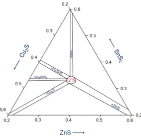
Secondary phase formation in CZTS
Secondary phases can arise from non-optimal film composition that lies outside the single phase region (SPR), as can be seen in figure 2. Based on the article by Siebentritt et al. (2012) a maximum deviation from stoichiometric composition of 1-2 at.-% allows the existence of a SPR. Secondary phases can also form during the annealing of CZTS precursors. The rather low stability of Sn (+IV oxidation state) makes the CZTS prone to decompose during the anneal due to reduction of Sn to oxidation state +II. The Sn-S bonds break and S atoms are extracted from
the CZTS leading to the formation of secondary phases such as Cu2S, SnS and
ZnS, as described in reaction 2 (Ren et al. 2017). The Sn-S phase decompose in steps from SnS2 to Sn2S3 to SnS via reaction 3. At the film surface the high vapor
pressure of sulfur at typical annealing temperatures drives the evaporation of S2(g)
and SnS(g), hence partial sulfur pressure in the process is an important parameter
to control the decomposition of the Sn-S phase and therefore also the CZTS phase (Ito 2014). At the back of the film, S reacts with the Mo back contact and forms
MoS2. The sulfur gets extracted from either the CTZS phase or the secondary
phase SnS2 (ibid.). Cu2ZnSnS4(s) −−*)−− Cu2S(s)+ ZnS(s)+ SnS(g)+ 1 2S2(g); SnS(s) −−*)−− SnS(g) (2) 2 SnS2(s) −−*)−− Sn2S3(s)+ 1 2S2(g); Sn2S3(s) −−*)−− 2 SnS(s)+ 1 2S2(g) (3)
The formation of the ZnS phase is driven by diffusion that occurs when the con-centration of Zn reaches beyond the limit of solubility in CZTS. It has been shown
to occur when the composition is Zn-rich, Zn/(Cu + Sn) > 13 suggesting that
the formation of ZnS is mainly dependent on composition (Just et al. 2016). It forms at the back contact during the first minute of annealing before formation also starts at the surface as shown in Ren (2017). The formation of ZnS on the films surface is promoted by the surface decomposition of CZTS due to insufficient
partial sulfur pressure (Ren et al. 2017). The formation of the CuxS phase has
also been linked to composition of the CZTS material with segregation starting at a Cu/Sn > 2 (Just et al. 2016).
Figure 2: Central part of the ternary phase diagram for CZTS. In the middle lies the SPR for CZTS and branching out are the compositional regions where secondary phases also are present.
2.3
Analysis techniques
The theory behind the chemical and optical characterization tools used in this study is presented in this section.
2.3.1 Energy dispersive x-ray spectroscopy
EDS relies on the interaction between charged particles, in this case electrons, and the samples atoms. Each unique atomic structure has a characteristic set of peaks in its electromagnetic emission spectrum. This fundamental principle is what allows identification of elements (Goldstein et al. 2017). In short, the incoming high energy particles have a possibility to excite electrons in the atom’s inner shells leaving an electron-hole behind. When that electron relaxes back to its original, unexcited state it releases a photon with energy depending on the difference in energy between the shells. This emitted photon yields a unique signal in the EDS spectrum depending on the atomic structure, much like a fingerprint (ibid.).
2.3.2 Photon-Crystal lattice interaction, Raman and
photoluminescence The Raman effect
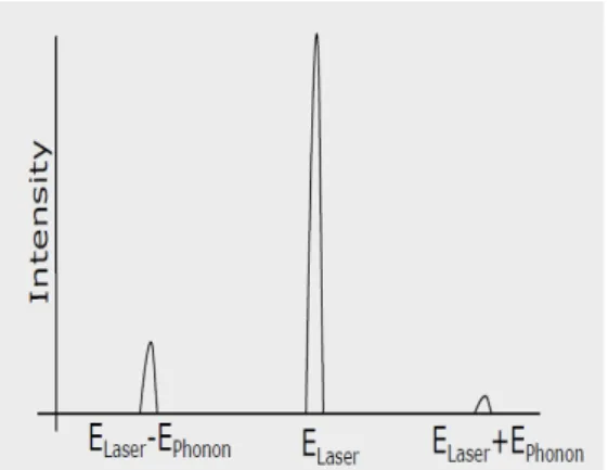
The Raman effect, named after its discoverer C.V. Raman, originate from the interaction between incoming photons from a light source and phonons in the material (Loudon 1964). When light gets scattered by a material it mainly contains the wavelengths that were incident on the sample but some other wavelengths are also present at very low intensities: a few parts per million or less compared to the main signal. This represents an interaction with the material and is what is called the Raman effect (Schroder 2006). In figure 3a basic scattering processes is shown and next to it in figure 3b the difference in energy shift for the mentioned scattering processes is shown. The Rayleigh scattering is an elastic process where the outgoing photon has the same wavelength as the incoming one. The Stokes scattering is an in-elastic process that imparts energy on the crystal lattice in the form of a phonon and in Anti-Stokes scattering a phonon from the lattice imparts its energy on an incoming photon (Rudisch 2016). It is possible for these in-elastic scattering processes to impart several phonons worth of energy on the crystal lattice or vice versa: with decreasing probability for each extra phonon. It is then called 1st order for one phonon and 2nd order for two and so on. These higher order scattered photons show up in the Raman spectrum as peaks at higher frequencies, exact position is dependent on the phonons imparted. The Anti-Stokes mode is much weaker than the Stokes mode, therefore it’s usually the Stokes scattering process that’s monitored in Raman spectroscopy by comparing the incoming light with the outgoing (Schroder 2006). The unique atomic structure of each compound
results in characteristic shifts in energy of the scattered light. This can be seen in a Raman spectrum obtained via Raman spectroscopy as Raman peaks characteristic to the compound, each compound having its own unique "fingerprint" (Schroder 2006). Some compounds have overlapping Raman peaks due to similar atomic structure, making differentiation more difficult.
(a) Basic scattering processes of light. The scattering can in short be described in three steps. 1: A photon excites an electron in the material. 2: The ex-cited electron interacts with the lattice structure and creates (Stokes) or ab-sorbs (Anti-Stokes) a phonon. 3: The electron recombines and releases a pho-ton.
(b) Intensity of energy shift of scattered light from the basic scattering processes seen in figure 3a. Starting from the left is the Stokes scattering, next is the Rayleigh scattering and last is the Anti-Stokes scattering.
Figure 3: Permission is granted by the copyright holder Katharina Rudisch to use and modify these pictures taken from her presentation on sub phase analysis of
Cu2MnSnS4 with multi-wavelength Raman spectroscopy from 2016 (Rudisch 2016).
The use of Raman spectroscopy serves as a powerful tool to characterize crystal structures and identifying the presence of secondary phases. The standard exci-tation wavelength in Raman spectroscopy is 514 or 532 nm. In investigation of kesterite phase CZTS it yields a large number of Raman peaks with relativity low intensities making it hard to determine the different peak positions and also identifying secondary phases. Instead, using an excitation wavelength of 785 nm results in a resonance effect for certain kesterite phase CZTS Raman modes, mak-ing them several magnitudes more intense than the modes of secondary phases possible present in the material (Dimitrievska 2015). The resonance effect occurs when the energy of the excitation source is near the required energy for electronic transition to the conduction band to take place (Strommen et al. 1977). A
com-pound’s conduction band structure can be composed of several energy states to which an electronic transition can occur, leading to it having several possible points of resonance (Dimitrievska 2015). For CZTS these points of resonance occur at the band gap and at an energy level of 3.50 eV. Identification of secondary phases, using the resonance effect, in kesterite phase CZTS requires the use of other
ex-citation wavelengths, with the exception of the Cu3SnS4 phase which also shows
a high intensity in Raman spectra when using 785 nm excitation wavelength due to the resonance effect (ibid.). Using UV excitation (325 nm) for example yields a near resonance effect for the compound ZnS which is a common secondary phase in off-stoichiometric CZTS materials. This makes identification of the phase rela-tively easy (ibid.).
The Raman spectra peak intensities and their corresponding position give valu-able information about the sample. The intensities give information about the material’s electronic properties, its band structure etc. and the peak position give information about the mechanical properties of the crystal like atomic masses, bond strengths, geometry etc. Analyzing the shift in observed peak position com-pared with the expected one can give information about strain and stress in the crystal structure. The width of the peak also contains information, giving a hint about the crystal quality of the material for example
Photoluminescence
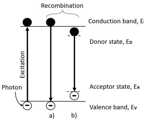
Photoluminescence occurs when a photo-excited electron relaxes back to its orig-inal state and emits a photon with wavelength corresponding to the difference in the excited and unexcited energy state (Schroder 2006). This is what is called ra-diative recombination. Non-rara-diative recombination can also occur in a material. The excitation energy then dissipates via other forms of energy, such as heat or by inducing lattice defects in the crystal structure (Pelant et al. 2012). A material’s photoluminescent behavior can give an indication of how well it is suited for PV applications by measuring its radiative recombination. In impure materials several radiative recombination routes are possible, the most common ones for kesterite CZTS are shown in figure 4 (Schroder 2006).
At room temperature the band to band recombination, figure 4(a) dominates
(ibid.). Recombination between the materials acceptor- and donor states,
fig-ure 4(b) originating from the materials impurities or defects occur as well but are weakly pronounced at room temperature. For kesterite phase CZTS the abundant
Figure 4: Observable radiative recombination routes with room temperature pho-toluminescence spectroscopy.
presence of structural defects and impurities seem to entail potential fluctuations in the band gap structure, altering its shape (Van Puyvelde et al. 2015). Therefore band to band recombination is seldom observed. Further, the high density of de-fects aggravate clear definition of donor- and acceptor energy states. In conclusion, what mode of recombination one observes in CZTS is hard to define. This topic is widely discussed in the research community, see for example the articles by Lang et al. (2017) and Van Puyvelde et al. (2015). Measuring photoluminescence is performed in the same way and with the same equipment as Raman spectroscopy, described in the section above. The obtained spectrum can be analyzed by iden-tifying the peak position and its intensity. Giving information about how much radiative recombination occurs in the material and comparing the peak position with the expected band gap for the investigated material can give information regarding the presence of defect states (Schroder 2006).
3
Method
Four combinatorial and polycrystalline samples were prepared with different an-nealing procedures and investigated using the optical characterization methods, Raman and photoluminescence spectroscopy. This optical characterization was then analyzed based on compositional data from EDS provided by the supervisor. The fabrication and characterization techniques used in the study are described in more detail in the following section.
3.1
Preparation of samples
As mentioned before, the to date most successful production route for CZTS thin films is a two-stage process. Starting with precursor deposition at low temperatures
(∼250◦C) followed by a high temperature (∼ 400−600◦C) anneal and thereafter a
low temperature thermal treatment, yields devices with as high as 12.6 % efficiency (Wang et al. 2014). A similar two stage production route is used in this study.
3.1.1 Precursor deposition
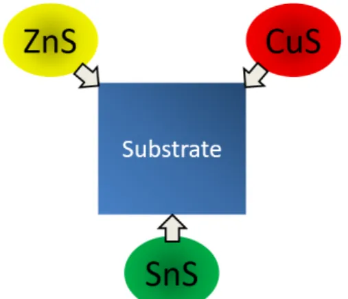
Substrate dimensions were 7×7 cm and precursors were produced using pulsed DC co-sputtering with compound targets. CuS, SnS and ZnS-targets were positioned in a triangular configuration pointing towards the center of the substrate holder with an angle of 45◦, see figure 5b. The sputtering progressed under 0.7 Pa pressure with a constant flow of argon at 50 sccm and at a substrate temperature of 225◦C. The target material was deposited on a soda-lime glass substrate coated with Molybdenum, a commonly used back contact material for thin film solar cells. A Kurt J. Lesker deposition chamber, see figure 5a, was used for sputtering and the time was set to 25 min, yielding a film of roughly 500 nm thickness. To be able to investigate a wide range of compositions the substrate holder was not rotating during the process. That way a compositional gradient could be obtained across the samples.
(a) Reactive co-sputter, Kurt J. Lesker system.
(b) Compound target configuration in the deposition chamber.
Figure 5: In a) one can see the Kurt J. Lesker system used in the deposition. In b) is a representation of the targets triangular configuration in the deposition chamber.
3.1.2 High temperature anneal
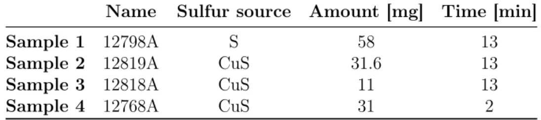
Before annealing in a tube furnace, 5×5 cm pieces were cut from the sample’s tin-rich side which was visually identified. This due to the limitation of size introduced by the coated graphite box used in the process. These boxes have a submerged area to load the sample on which is surrounded by a rim containing four small "pockets" placed in the middle of each side. In these an amount of a chosen sulfur source was placed to create a sulfur enriched atmosphere during the process. See table 1 for detailed information regarding the samples different annealing condi-tions.
The anneal, also called recrystallization process was performed under a stable argon atmosphere at a pressure of 350 torr. After loading the sample in the load lock, a standard cleaning procedure was performed to avoid air contamination in the system. Afterwards the sample plate was pushed into the cold zone using the so called transfer rod. Afterwards the sample was transferred from the cold zone
to the hot zone where the sample plate temperature rose from 35 − 550◦C during
a 70 − 80 s period. When the sample plate had reached a temperature of 550◦C
the annealing timer was started. After about 600 s the sample’s temperature had
stabilized at roughly 580◦C, which was the maximum achieved in the process. At
the end of the anneal the sample was transferred back to the cold zone to cool
system.
Table 1: Annealing conditions for investigated samples
Name Sulfur source Amount [mg] Time [min]
Sample 1 12798A S 58 13
Sample 2 12819A CuS 31.6 13
Sample 3 12818A CuS 11 13
Sample 4 12768A CuS 31 2
3.1.3 Post-anneal ordering treatment
To enhance the Cu-Zn ordering in the crystal structure, the samples were subjected to a low temperature thermal treatment after the high temperature anneal. The thermal treatment was performed in the same tube furnace, using the same kind of coated graphite box as the high temperature anneal, but at a pressure of 300 torr in a stable argon atmosphere. The graphite box was loaded with the sample as well as some elemental sulfur (37 − 50 mg) to sustain a sufficient partial sulfur pressure during the process. After transferring the sample to the hot zone, the
sample plate temperature ramped from 25 − 265◦C. When the sample plate had
reached a temperature of 265◦C a timer of 3 min was initiated, after which the
slow cooling of the sample begun at a rate of 0.1 K/min. The set temperature was
programmed to ramp down from 300 − 80◦C and at the given cooling rate this
ramp down took roughly 37 h.
3.2
Characterization of samples
To characterize the samples several methods were used. In all methods a mapping approach was chosen. The mapping was done as a raster on the samples surface, leaving a rim unmeasured. This was to avoid the edges to affect the measurements. In the EDS measurements an area of 4×4 cm was mapped and in the Raman and photoluminescence measurements an area of 3.8×3.85 cm was mapped. The difference originate from the two setups’ different configurations.
3.2.1 Elemental analysis
The samples’ elemental composition was determined using a Scanning Electron Microscope (SEM) setup with an incorporated EDS facility. The setup used was a LEO 1550 SEM. The measurements were performed by the project supervisor, Katharina Rudisch.
The composition was measured after the first anneal for all samples to make com-parison easier. The sample was placed in a vacuum chamber and aligned in such a way that the measurement points would correspond well with the optical char-acterization measurements described further down in the section optical tools. A step-size of 2.01 mm in x-direction and 1.51 mm in y-direction were used, resulting in 540 data points. Based on the overlap of Sn and Ca peaks in the electromag-netic emission spectrum, Ca was included along with Cu, Zn, Sn in the fitting of the emission peaks to enhance the fitting of the Sn peak. The setup used has been shown to overestimate the Zn content and underestimate the Cu content by 1 − 2 at.-% on average respectively. In Ericson (2013) a comparison between the setups measurement and a x-ray fluorescence (XRF) measurement is used to show this measurement error.
The data from the EDS mapping was then analyzed by Luciano Quaglia Casal, another master student at the department, as a part of his thesis project. His analysis results were used in this thesis project.
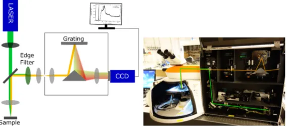
3.2.2 Raman and photoluminescence spectroscopy setup
To investigate the crystal structures of the samples, multi-wave Raman spec-troscopy and single-wave photoluminescence specspec-troscopy was performed using a Renishaw InVia Raman microscope equipped with four different lasers: a 325 nm (UV), a 532 nm (green), a 633 nm (red) and a 785 nm (infrared). The measure-ments were acquired on the same data points as in the compositional analysis to be able to correlate composition with the Raman and photoluminescence results. A step-size of 2.00 mm in x-direction and 1.50 mm in y-direction were used during mapping. To avoid damaging the samples and therefore changing its properties, precautions were taken regarding laser intensity, also exposure time was adjusted to acquire a signal of sufficient intensity.
The setup had a back-scattering Raman configuration, meaning that the scat-tered photons travel the same path as the incoming ones, the setup can be viewed
in figure 6. The excitation photons were focused on the sample’s surface by a microscope objective. For mapping purposes, the 5× objective was chosen and for identification of SnxSy phases, described in detail in the result section, the
50× magnification was used. The scattered photons were then reflected towards the photo detector, in this case a Charge-Coupled Device (CCD) camera. Before reaching the camera, the scattered photons were passed through an edge filter to cut off the wavelengths close to the one of the excitation source in order to protect the detector. Then the photons were reflected onto a diffraction grating in order to disperse the light before detection of individual wavelengths in the CCD cam-era. Depending on the excitation wavelength different edge filters and diffraction gratings had to be used. The resolution of the acquired spectrum was dependent on the excitation wavelength, the edge filter and the diffraction grating. In table 2 the different gratings used in this study are listed, also the different edge filters’ specific cut off frequencies and the resolutions of the particular setups are included in the table. The resolutions were approximated by looking at the Si peak in the calibration spectra along with discussions with the project supervisor. The ap-proximation was based on the assumption that the Si sample was of high purity and that the width of the peak was mostly dependent on the setups resolution.
(a) A sketch illustrating a Raman setup. (b) A picture of the Raman setup used in this study.
Figure 6: Permission is granted by the copyright holder Katharina Rudisch to use and modify these pictures taken from her presentation on sub phase analysis of
Table 2: Raman setup for different excitation wavelengths
Excitation Grating Edge filter Resolution
wavelength cut off
[nm] [lines/mm] [cm−1] [cm−1] 785 1200 ∼80 ∼2.0 633 1800 ∼90 ∼2.0 532 1800 ∼90 ∼2.0 325 2400 ∼200 ∼5.0 532 (PL)* 1200 ∼1.1e−2eV ∼5.0e−4eV
*It should be noted that the setup configuration is altered for PL measurements and that the unit is eV instead of cm −1.
Before analyzing the obtained Raman spectra, some operations needed to be done. Foremost the spectra were truncated, leaving only the parts containing information from the sample. The truncation interval chosen differed depending on the laser used to produce the spectra. Secondly, the cosmic rays contaminating the spectra were removed using the Windows-based Raman Environment (WiRE) software’s function to automatically identify cosmic rays as well as visual inspection. Lastly, the background was removed by fitting a polynomial of degree 11 to chosen points in the spectra and subtracting it from the signal.
Sample alignment
The samples were placed on a stage with possibilities to align it in all 3 space dimensions (X, Y and Z). Using screws to adjust the height alignment (Z-direction) and a rotatable section in the middle of the stage to adjust the planar alignment, in X and Y direction.
The planar alignment was done by visual estimates, setting the origin of the co-ordinate system in the reference corner and moving the stage 20000 µm in the X-direction while keeping the Y coordinate static. Then moving the camera’s (in-cluded in the Renishaw InVia Raman Microscope) cross hair in Y-direction to the sample edge in order to evaluate the deviation. A maximum deviation of ±100 µm was chosen as the limit. This alignment was performed in the beginning of each measuring session and also if changing the sample during a session.
The height was aligned by finding the optimal focus of the 532 nm laser on all four corners and comparing the values on the Z-axis. The Z-position yielding the
highest intensity was assumed to have the optimal height alignment. The laser dot was also inspected by visual estimates as an extra precaution since it was observed that the intensity also was dependent on the alignment of the laser itself, giving rise to false results. The maximum allowed discrepancy of the 4 corners was chosen to be ±50 µm with regards to the reference corner. This was done to avoid using the setup’s built-in focus tracker which proved not suited for some measurements, due to it also using the intensity of the signal to find the optimal focus.
Photoluminescence Spectroscopy
The method used to identify the samples’ photoluminescence were similar to the Raman measurements, also the sample alignment was the same. The acquisition time of photoluminescence spectra are longer than for Raman, in the range of 2.5 min for each data point. This brought the need to divide the mapping of an entire sample into two measurement sessions since the total time for one map would amount to roughly 22.5 h. The 532 nm laser, an edge filter with cut off
at ∼200 cm−1 and a diffraction grating with 1200 lines/mm were used to acquire
the photoluminescence spectra. Difficulties to find a combination of laser intensity and exposure time suitable for all data points on the samples led to overloading of the photo detector for some data points with strong PL signal. Complimentary measurements on these points using a lower laser intensity had to be made for easier identification of the PL peak position.
The raw spectra were analyzed using Matlab after cosmic ray removal and sub-traction of the background. Some data points lacked PL signal and the one with lowest intensity was assumed to be a good representation of the background signal. This spectrum was identified separately for each sample and subtracted from the data sets. In Matlab the background subtracted spectra were smoothed five times using a moving average filter with a span of five data points to remove some of the noise and make identification of peak positions simpler. The peak positions were identified by simply finding the position of the maximum value of intensity in the data set. This value was also used to represent the peak intensity of that measurement point. The smoothing may have introduced a shift in peak positions, this is further discussed in the result section.
4
Results and discussion
4.1
Compositional analysis
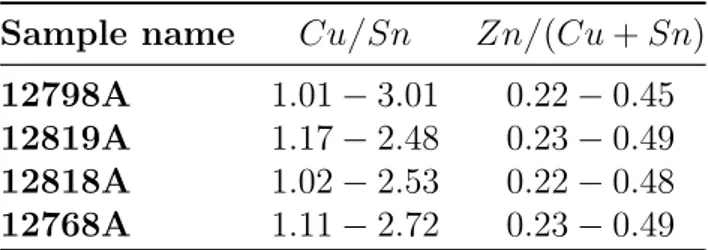
The compositions of the samples were investigated using EDS mapping, as de-scribed in more detail in previous sections. The raw data from the mapping was fitted by Luciano Quaglia Casal, another master student at the department, as a part of his thesis project. His fitting results are what I use in my analysis in order to connect sample composition and annealing conditions to changes in the samples. The fitting results and the method used to produce them will be shown in its entirety in his project report. In table 3, the acquired ranges of composition for the four samples investigated are presented.
Table 3: Composition ranges obtained via EDS analysis for all samples in the study.
Sample name Cu/Sn Zn/(Cu + Sn)
12798A 1.01 − 3.01 0.22 − 0.45
12819A 1.17 − 2.48 0.23 − 0.49
12818A 1.02 − 2.53 0.22 − 0.48
12768A 1.11 − 2.72 0.23 − 0.49
4.2
Components of a CZTS Raman spectrum
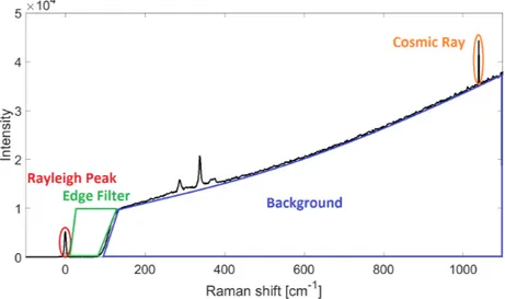
In figure 7 a CZTS Raman spectrum obtained with a 785 nm laser source is shown. One can observe what is left of the Rayleigh peak at 0 cm−1 after filtering, also the cut-off of the edge filter at around 90 cm−1 is clearly visible. Further, one can observe the background caused by the excitation source and the crystals’ photoluminescence. It should be noted that this photoluminescence is not present
in all Raman spectra. Also, note the sharp peak at about 1000 cm−1. This signal
originates from the cosmic background radiation and are best identified by looking at its small width compared to the other peaks present. They can be prevented by doing multiple accumulations and comparing the spectra to identify the presence of a cosmic ray or by removing them by hand after obtaining the spectrum. All Raman spectra, independent of excitation wavelength are composed of these four characteristic components.
Figure 7: Typical Raman spectrum for CZTS obtained with 785 nm laser source with its characteristic parts marked. Marked in red is the Rayleigh peak, in green the cut off by the edge filter, in blue the background and in orange a signal from the cosmic background radiation.
The CZTS material has 11 characteristic Raman modes in the interval 200-500 cm−1
(Khare et al. 2012). Their expected Raman shifts are pointed out in figure 8a. The
most intense ones are found at Raman shift 305 cm−1 and 339 cm−1. The
charac-teristic peaks are more or less visible depending on the wavelength of the incoming excitation source. They are most easily observed with the use of 785 nm excitation due to the resonance effect. Identification of secondary phases have been done by searching for Raman peaks distinguishable from the CZTS peaks.
4.3
Secondary phase identification
When investigating a combinatorial CZTS sample one expects a few secondary phases to be present. The ones expected and therefore searched for in this study are Cu3SnS4, Cu2SnS3, CuxS, SnS, SnS2, Sn2S3 and ZnS, based on the elements
present in the sample and earlier work about the material (Ito 2014). These
secondary phases along with the CZTS phase can be seen in table 4 with their
respective Raman peaks used to identify them. The CuxS phase has many stable
Cu/S-ratios which according to literature have overlapping Raman peaks (Munce et al. 2007). A brief investigation of the spectra available in the RRUFF database supported this claim (RRUFFProject 2018b)(RRUFFProject 2018a). Therefore no attempt to distinguish between them have been made in this study.
Table 4: Most common secondary phases in the CZTS-system and their respective Raman peaks. The most pronounced Raman peaks of the compounds are written in bold text.
Phase Raman peaks [cm−1]
Cu2ZnSnS4 [1] 252, 266, 278, 290, 305, 316, 332, 339, 353, 368, 377 Cu3SnS4 [2] 321 Cu2SnS3 [3] 297 CuxS [4] 264, 475 SnS [5] 163, 189, 220, 288 SnS2 [5] 215, 312 Sn2S3 [6] 234, 251, 307 ZnS [7] 351
[1](Khare et al. 2012), [2](Davydova et al. i.m.), [3](Lund et al. 2014), [4](Fernandes
et al. 2011),[5](Parkin et al. 2001) , [6](Price et al. 1999),[7](Ito 2014)
Cu3SnS4
To identify the Cu3SnS4 phase the spectra acquired with the 785 nm laser were
analyzed. The compound has a band gap of 1.60 eV (Fernandes et al. 2010). Figure
8b shows a spectrum with an apparent Cu3SnS4 peak. Just as the CZTS phase,
it shows a resonance behavior with the 785 nm laser. The presence of Cu3SnS4
was identified by integrating the intensity of the Raman signal in the window
316 − 327 cm−1. Although the Cu3SnS4 main peak is separable from the CZTS
(a) (b)
Figure 8: Raman spectra acquired from a combinatorial CZTS sample with a 785 nm laser. In a) one can see a Raman spectrum containing the positions of the 11 characteristic peaks of CZTS. In b) one can see a spectrum containing CZTS and the secondary phase Cu3SnS4 with a peak at 321 cm−1.
ZnS and CuxS
To identify the phases ZnS and CuxS, the spectra acquired using a 325 nm laser
were analyzed. ZnS and CuxS have a band gap of ∼ 3.7 eV and ∼ 1.2 eV
respec-tively (Ito 2014). The UV-light does not penetrate the material deeply, thus this method is surface sensitive (Zoubir 2012). The implication of this surface depen-dence will be discussed later in the report. The presence of CuxS was identified by
integrating the intensity of the Raman signal in the window 469-477 cm−1. And,
the presence of ZnS was identified by integrating the intensity of the Raman signal
in the window 685-705 cm−1, capturing the 2nd order peak which does not
over-lap severely with the CZTS peaks (Davydova et al. i.m.). In figure 9a a typical spectrum containing only the CTZS and the ZnS phase is shown. CZTS interacts poorly with 325 nm light while ZnS shows a resonance effect, this due to its band gap of about 3.88 eV (Ericson 2013)(Borah et al. 2008). In the spectrum, Raman peaks corresponding to 1st, 2nd and 3rd order phonons are visible. The visibility of at least the first two was used to underwrite the presence of ZnS. In figure 9b
both Raman peaks corresponding to CuxS are apparent alongside the ZnS peaks.
Also, a peak at around 780 cm−1is visible. This peak is system related and thus do
not contain information regarding the sample. The peak at 475 cm−1 was observed
to be the most pronounced one. Therefore, it was used as the main indicator of CuxS being present in the films.
(a) (b)
Figure 9: Raman spectra acquired from a combinatorial CZTS sample with a 325 nm laser. In a) one can see a Raman spectrum containing the ZnS peaks. In
b) one can see a spectrum containing ZnS and the secondary phase, CuxS with a
peaks at 264 cm−1 and 475 cm−1.
SnxSy
The SnS2 phase was observed on the different samples’ surfaces in the UV
Ra-man spectra, see figure 10. Nevertheless, the use of UV RaRa-man mapping is not suitable for accurate identification of the SnxSy phases since they have a tendency
to accumulate at the samples’ back contact (Ren et al. 2017). Therefore, another
approach was taken to identify the SnxSy phases. The approach is described in
more detail further down in the report. With this said, a comparison between
the SnS2 present at the surface and at the back contact may provide information
regarding the partial sulfur pressure during the anneal. The previous statement is
based on the fact that the loss of surface bound SnS2 through evaporation of SnS
and S during the anneal is influenced by the partial sulfur pressure, as shown in (ibid.). SnS2 has a band gap of ∼ 2.5 eV and SnS has a direct band gap of ∼ 1.3 eV
and an indirect one of ∼ 1.0 eV (Ito 2014).
As stated earlier SnS and SnS2are known to accumulate at the back contact, hence
this mapping method was not suitable to detect them (Ren et al. 2017). Instead
another approach was taken. As a last step of the optical measurements the
samples were scribed using a scalpel, exposing the back contact. The scribed lines were then examined using the Raman setup with a 50× magnification objective and the 532 nm laser. Through the naked eye, flakes that might be of interest were identified. In figure 11a one can see a few flakes of interest and in figure 11b one can see a flake, glowing slightly in a bluish color under the microscopes
Figure 10: Raman spectra acquired from a combinatorial CZTS sample with a 325 nm laser. In the figure one can see a spectrum containing ZnS and the secondary phase SnS2 with a peak at 312 cm−1
illumination. This glow was interpreted as an indication of the flake being a SnS crystal. The glow might originate from the crystals photoluminescence, although no report could be found to support this claim. Thus, this assumption is open for further debate and investigation. It may be that the glow simply originates from the setups illumination being reflected on the flakes surface. The colored rings on figure 11a encircle three flakes that measurements were performed on and the measurements respective names. Further, the size of the laser spot and
the penetration depth of the laser entailed the presence of MoS2 Raman peaks
in all measurements, which can be seen in figure 12 and 13. An investigation of
MoS2 Raman modes was performed by Sandoval et al. (1991). In the report it is
suggested that the MoS2 phase has 1st order Raman modes at 156, 226, 287, 333,
383, 408 cm−1. The authors also observed Raman peaks at 454 and 639 cm−1 which
were assumed to be 2nd order Raman peaks. A brief investigation of the available
MoS2 Raman spectra in the RRUFF database showed Raman peaks at the same
positions, in accordance with Sandoval et al. (ibid.) (RRUFFProject 2018c). In figure 12 the three above mentioned measurements on the flakes in figure 11a
are shown and certain peaks corresponding to SnxSy phases and MoS2 have been
marked out. The increased intensity in the range 270 − 370 cm−1 for the red
spectrum (R0477), compared to the others, may be explained with possible ZnS presence at the back contact. The presence of ZnS at the back contact has been shown in Ren et al. (2017). Also, the apparent peak at 333 cm−1 may be attributed to ZnS in its cubic phase. As suggested in Nilsen (1969) cubic phase ZnS has 1st
order Raman modes at 88, 110, 306 and 333 cm−1. ZnS in its cubic phase is
not expected to present in the samples. Hence, other explanations for the red spectrum’s appearance may be more valid. Nevertheless, with the two presented
(a) (b)
Figure 11: Pictures taken with the microscopes built-in camera. In a) a large number of flakes are visible. Measurements were taken on the encircled flakes. The picture was taken using 50× magnification. In b) a flake glowing in a bluish color is present. The glow was observed to be an indication of it being a SnS flake. The picture was taken using 5× magnification
studies in mind it is possible that measurement R0477, the red line in figure 12,
was performed on a flake composed of SnS, SnS2 and cubic phase ZnS. The other
two flakes were identified as being composed of both SnS and SnS2. The observed
shift in peak position of some Raman peaks in relation to the theoretical ones are attributed to the Raman setup’s resolution, see table 2 for information regarding the resolution of different measurement configurations.
Figure 12: Raman spectra of three different flakes, encircled in figure 11a obtained with an excitation wavelength of 532 nm.
In figure 13 the spectrum acquired on the flake (blue line) in figure 11b together with a spectrum acquired on the back contact (red line) next to it where no flakes were visible are shown. The small size of the flake and its location just on the edge of the scribing line entailed the presence of the CZTS main Raman peak at 338 cm−1. Further, the small size may be the cause of the weak SnS Raman signal.
Since the SnS Raman peaks at 220 cm−1 and 288 cm−1 overlap with the ones of
MoS2, the SnS Raman peak at 187 cm−1 was used as the main indicator for the
presence of the SnS phase.
Figure 13: Raman spectrum of the blue flake in figure 11b is presented in blue and a spectrum obtained on the back contact next to the flake is shown in red. No offset has been applied to accentuate the more intense background present for the blue flake.
4.4
Distribution of secondary phases
The distribution of secondary phases was investigated to identify the Single Phase Region (SPR) of the samples. The SPR is expected to be present around the stoichiometric point of CZTS, which is at Zn/(Cu + Sn) = 0.33 and Cu/Sn = 2. The CZTS phase itself was observed for all compositions across the samples. Maps such as shown in figure 14 were used as well as visual inspection of the spectra to determine the distribution. Larger drops of the heat map’s intensity were used as a first approximation of the distribution of the secondary phases before visual in-spection of the Raman spectra commenced for more accurate identification. Since
the approach was identical for all samples only maps representing the reference, 12798A will be shown here. The maps from samples 12819A, 12818A and 12768A can be found in the appendix 1. The maps were produced by integrating the intensity in narrow interval around the expected Raman peak position for each re-spective secondary phase and were correlated with the sample composition using the cation ratios, Zn/(Cu + Sn) and Cu/Sn.
The distribution of Cu3SnS4 was identified by integrating the intensity of the
Raman signal in the window 316 − 327 cm−1. In figure 14a one can see an area
of high intensity in the region of Zn-poor composition, approximately stretching between 1.20 < Cu/Sn < 2.15. The intensity variations across the rest of the map are related to changes in the intensities of the CZTS Raman peaks. This distri-bution of Cu3SnS4 is in accordance with Davydova et al. (i.m.) findings. Similar
distribution was observed for all samples in this study, see appendix 1. On sample 12819A the distribution was shifted slightly towards the region of Zn-poor com-position. This could be due to the overestimation of the sample’s Zn-content or due to the amount of sulfur in the anneal, sustaining a sufficient partial sulfur pressure during the process. The similarity of the distribution of Cu3SnS4 for the
samples can be an indication that the formation of this phase is not affected by the annealing conditions but rather by the composition.
The distribution of CuxS was identified by integrating the intensity of the
Ra-man signal in the window 469-477 cm−1. In figure 14b an area of high intensity in the region of Cu-rich composition is visible. The formation seems to start when the Cu/Sn ratio is above ∼2.1 and similar distributions were observed for the other
samples, see appendix 1. This indicates that the formation of CuxS is mostly
dependent on composition and not on the annealing conditions. The intensity variations across the rest of the map are attributed to the measurement’s signal to noise ratio.
The distribution of ZnS was identified by integrating the intensity of the Raman signal in the window 685-705 cm−1. In figure 14c an area of high intensity in the region of Zn-rich composition is visible. At 1.8 < Cu/Sn ≈ 2.0 the ZnS phase is observable for Zn/(Cu + Sn) ratio above 0.36. For lower or higher Cu/Sn ratios the ZnS phase is observable at Zn/(Cu + Sn) ratios below 0.36, as far as 0.3 in the region of Sn-rich composition. Similar distributions were observed in these lower or higher Cu/Sn ratios for the other samples. This might be an indication that the CZTS phase is unstable in these composition regions and that it partially decomposes into secondary phases. Regarding the presence of the ZnS phase at 1.8 < Cu/Sn ≈ 2.0 for the other samples, some differences can be seen. This
indi-cates that the formation of the ZnS phase in this composition region are affected by the annealing conditions. These will be discussed further in the upcoming SPR section. The intensity variations across the rest of the map are attributed to the measurement’s signal to noise ratio.
The distribution of SnS and SnS2 was determined using the scribing approach
described in the earlier sections. The distribution of SnS2 was determined to be
sufficient to identify the SPR for sample 12818A and 12819A since it stretched further towards the Cu-rich side than the SnS, hence the distribution of SnS was omitted from their respective SPR investigations. For sample 12798A only the
SnS phase was observed and on the contrary only the SnS2 phase was observed
on sample 12768A. This is due to the anneal times of 2 min. Since the decrease in partial sulfur pressure is key to the decomposition of SnS2 it can be concluded
that it was kept sufficient during the first 2 min of the anneal, in accordance with (Ren et al. 2017). In Ren (2017) they propose that the decomposition starts after 5 min of anneal for anneals using ∼40 mg elemental sulfur as the sulfur source.
(a) (b)
(c)
Figure 14: Intensity of Raman spectra in regions of typical Raman peaks for certain secondary phases on reference sample with respect to composition. Note that the scale of the heat map is logarithmic for the integration results. The inten-sity of the Cu3SnS4 peak, the CuxS peak and ZnS peak is shown in a), b) and c),
4.5
Identification of the single phase region
Via the investigation of the different secondary phases’ distribution across the sam-ples, an approximation of their respective SPRs’ could be defined. This was done by plotting lines on their respective composition maps, corresponding to where on the samples the different secondary phases could no longer be observed. The defining of the borders was done using the method mentioned in the previous sec-tion. That is, using heat maps such as in figure 14 for an approximation of the different phase borders. And afterwards, visually inspecting the Raman spectra around the approximation for observable Raman peaks corresponding to the differ-ent secondary phases. The samples’ respective secondary phase borders and SPRs can be viewed in figure 15. It should be noted that the accuracy of Raman spec-troscopy, used to identify the secondary phases, are limited by the resolution of the respective setup configuration used to identify the different secondary phases distributions as well as the depth sensitivity of them. Also, the signal to noise ratio limited the identification in spectra with overall low signal intensity. There it sometimes was hard to differentiate possible peaks from the noise. Further, small crystal grains or grains present deeper in the films bulk may not have been detected via these methods, thus the real SPR may in fact be smaller than what is presented here. Furthermore, the suspected overestimation of Zn and underes-timation of Cu in the composition analysis should result in a shift of all identified secondary phase borders. This could explain why the SPRs observed are not cov-ering the stoichiometric point at Zn/(Cu + Sn) = 0.33 and Cu/Sn = 2.0.
The "tail" of the SPR towards the Cu-rich side, apparent in figure 15c and 15d raises questions about the secondary phase identification. Here, I will suggest some possible explanations, note that other explanations than presented can be
possible. Firstly, the UV Raman spectroscopy used to detect the CuxS phase was
relatively surface sensitive and hence unable to detect possible presence of the phase in the films bulk. This follows from the strong absorption of UV-light in the material, leading to the penetration depth of the light being small (Zoubir 2012). Secondly, the CuxS grains present at the surface for a Cu/Sn ratio less than 2.1
could have been of such a small size that the Raman signal was too weak for de-tection. Both would result in the border being shifted towards the Cu-rich side. In Davydova et al. (i.m.) the CuxS phase was shown to be present just after a Cu/Sn
ratio of 2.0, which supports the above theory. An investigation, as in Davydova et al. (ibid.), using SEM combined with EDS point measurements could be used to investigate the phase further and possibly show that the CuxS border in fact is
shifted. The above mentioned method would not be able to detect CuxS present in
of CuxS, possible missed in the investigation using Raman spectroscopy. Thirdly,
the overlap between the Cu3SnS4 Raman peak and the CZTS Raman peaks, as
mentioned earlier might have concealed the presence of Cu3SnS4 at the border
where its Raman signal was relatively weak. Thus, leading to a shift of the border towards the Zn-poor side. A more extended investigation using curve fitting could possibly shed some light on the subject. As will be seen further down in the PL section, the lack of a PL signal above the Cu3SnS4 border might also be viewed as
an indication of it being shifted. This follows from the expectation of no PL signal
from regions with CZTS and Cu3SnS4 phase, due to non-radiative recombination.
(a) (b)
(c) (d)
Figure 15: Phase diagrams for all combinatorial samples. The secondary phase borders are shown with dashed lines and an arrow indicating in which direction the phases are present. The SPR is indicated by ?.
4.5.1 Influence of annealing conditions/partial sulfur pressure on SPR and secondary phase formation
The small size of the reference sample’s SPR, seen in figure 15a is due to insuffi-cient partial sulfur pressure during the anneal. The elemental sulfur grains used in the anneal change to gas phase easily and escape from the graphite box, leaving the atmosphere unsaturated. According to Ren (2017) the evaporation of S and SnS from the CZTS thin film starts at around 5 min into the anneal for elemental sulfur anneals. Seeing that they introduced 40 mg in the anneal and in this study 58 mg were used, it is apparent that this amount is also insufficient to stabilize the sulfur pressure in 13 min anneals. On the contrary, the anneals with CuS seem to be able to sustain a S-enriched atmosphere during 13 min anneals, judging by the size of 12818A’s and 12819A’s respective SPR. The similar size of the SPR in figure 15b and 15c may indicate that the adequate amount of CuS to be used in the anneal process lies between 11-31 mg or even below 11 mg. The samples also show similarity regarding their composition, which further supports this indication. The different lower limit of the Cu/Sn ratios towards the region of Sn-rich composition, ∼ 1.2 for sample 12819A compared to ∼1.0 for the other samples, may be due to composition fitting of the EDS data. It could also be due to different deposition rates in the deposition of the samples.
For the sample 12768A, the short anneal time of 2 min resulted in a quite large SPR although the crystalline quality is expected to be poor (Ren et al. 2017). Further, the sample showed a large presence of surface bound SnS2, in accordance
with Ren et al. (ibid.) findings. The SnS2 phase was also the only one observed
at the sample’s back contact with the scribing method. These two observations indicate that the sulfur pressure was sufficiently high in the anneal.
4.6
Investigation of the CZTS cation disorder
The Q parameter was analyzed for the different samples. The parameter is
de-fined as the intensity ratio of the CZTS Raman peaks at 289 cm−1 and 305 cm−1,
i.e. Q = I289/I305. As in Davydova et al. (Davydova et al. i.m.) an integration
approach is used here, defining Q as, Q =R280295Idx/R302308Idx.
In figure 16 maps showing the Q values for all samples with regard to compo-sition can be seen. Also, the previously identified secondary phase boundaries are plotted on top. Between a Cu/Sn ratio of 1.8 and 2.1 the values tend to be in-creasing towards the region of Cu-poor composition, while being rather constant