A Master Thesis Work in Electronics
Development of a Multi‐bus platform for automation testbed
By
Lukas Knapik and Mathias Isaksson
Examiner: Professor Lars Asplund, Mälardalens University
Supervisor: Martin Ekström, PhD Student in Electronics, Mälardalen University
Dan Olsson, M.SC Physics, Infotiv AB
ABSTRACT
The task for this thesis was to develop, construct and evaluate a multi‐bus communication system, connected to a PC via USB and capable of communicating in CAN, I2C and SPI and develop drivers for it in National Instruments LabVIEW.
In the beginning a study was made of the communication buses followed by an investigation of what type of hardware that could accomplish this task. A microcontroller unit was selected and programmed in MikroElektronika MikroC Pro v.3.2 to act as the interface between the communication busses and PC. A PCB prototype of the system was constructed by using Eagle Cad software v.5.6.0. General drivers for this system where created in LabVIEW v.8.6.1 so the end‐user simply can create their own applications and control the compatible hardware depending on their type of purposes. The system was tested on criteria’s such as: speed, power consumption, burst performance and transmission length depending on which communication bus was used.
Development of a Multi‐bus platform for automation testbed Master Thesis CEL505
ACKNOWLEDGEMENTS
We would like to thank Infotiv AB for giving us the opportunity to do this thesis. A special thanks to our supervisors Martin Ekström at Mälardalens University and Dan Olsson at Infotiv AB for all their help and time they have dedicated to us.
Table of Contents
1. Introduction ... 1 1.1 Infotiv AB ... 1 1.2 Background ... 1 1.3 Purpose ... 1 1.4 Why Infotiv and this thesis ... 1 1.5 Delimitations ... 2 1.6 Deliverables to Infotiv ... 2 1.7 University Requirements ... 2 1.8 Timetable ... 2 1.9 The report layout ... 3 2. Bus study and research ... 4 2.1 The Inter‐Integrated Circuit Bus ... 4 2.1.1 Arbitration ... 6 2.1.2 Clock synchronization ... 7 2.2 The Control Area Network bus ... 7 2.2.1 The CAN protocol ... 7 2.2.2 CAN messages ... 8 2.2.3 CAN Errors ... 11 2.3 The Serial Peripheral Interface Bus ... 13 2.3.1 Data Transmission ... 13 2.3.2 Multiple SPI slaves ... 14 2.3.3 SPI drawbacks ... 15 3. Pre‐design circuitry considerations ... 17 3.1 Selecting an appropriate operations controller ... 17 3.2 Selecting an appropriate ADC ... 17 3.3 Power supply ... 18 3.4 Selecting ground ... 18 3.5 Protection against high voltage peaks ... 18 3.6 Diagnostics ... 18 3.7 Bus connectors ... 18 3.8 Schematics and PCB software ... 19 4. Circuitry components and design ... 20 4.1 Converter card components ... 20 4.1.1 Microcontroller – Microchip PIC18F4680 ... 20 4.1.2 USB UART Interface – FTDI FT232 ... 21 4.1.3 I2C Switch – Texas Instruments PCA9548A ... 21 4.1.4 I2C Accelerator – Linear Technologies LTC4311 ... 21 4.1.5 CAN Transceiver MCP2550 ... 22 4.1.6 Voltage Regulator REG1117‐5.0 ... 22 4.1.7 TVS Diodes ... 22 4.2 Converter card design ... 23 4.2.1 Power supply and ground ... 23 4.2.2 Setting up the FTDI circuitry ... 24 4.2.3 Setting up the MCU circuitry ... 24 4.2.4 I2C Switch Setup ... 25 4.2.5 I2C Accelerator setup ... 26 4.2.6 SPI setup ... 26 4.2.7 CAN setup ... 27 4.2.8 Converter card schematics ... 28 4.2.9 Converter card PCB ... 29 4.3 ADC Card ... 30 4.3.1 ADC Converter – Linear Technologies LTC2309 ... 30
Development of a Multi‐bus platform for automation testbed Master Thesis CEL505 4.3.2 I2C Accelerator – Linear Technologies LTC4311 ... 30 4.3.3 Setting up the ADC circuitry ... 30 4.3.4 ADC card schematics ... 31 4.3.5 ADC card PCB ... 31 4.4 PCB manufacturer and results ... 32 5. Software design ... 35 5.1 Microcontroller software ... 35 5.1.1 Main Menu ... 35 5.1.2 I2C ... 36 5.1.3 SPI ... 39 5.1.4 CAN ... 42 5.2 LabView drivers ... 48 5.2.1 Common Drivers ... 48 5.2.2 General I2C drivers ... 50 5.2.3 Special I2C Drivers ... 58 5.2.4 I2C ADC LT2309 Burst Drivers ... 62 5.2.5 General SPI Drivers ... 64 5.2.6 General CAN drivers ... 70 6. Results ... 86 6.1 The circuit boards ... 86 6.2 The LabVIEW drivers palette ... 86 6.3 GUI examples ... 88 6.3.1 ADC reading in burst mode ... 88 6.3.2 Writing and reading to components ... 88 6.3.3 Monitoring ... 89 6.4 Power consumption ... 90 6.4.1 Converter card power consumption ... 90 6.4.2 ADC cards power consumption ... 90 6.5 Signal performance ... 90 7. Performance Evaluation ... 92 7.1 Command execution time ... 92 7.1.1 I2C drivers execution time ... 92 7.1.2 SPI drivers execution time ... 93 7.1.3 CAN drivers execution time ... 94 7.2 Sampling rate from ADC ... 94 7.3 Optimal data transmission via UART ... 95 8. Improvements Possibilities ... 97 8.1 Electronics construction improvements ... 97 8.2 FPGA instead of MCU ... 97 8.3 Software programming ... 97 8.4 LabVIEW drivers ... 97 9. Discussion ... 98 10. References ... 99 10.1 Figure references ... 101 11. Appendix ... 107 11.1 Partlist ADC card ... 107
Development of a Multi‐bus platform for automation testbed Master Thesis CEL505
1. Introduction
In this section the master thesis project will be described and the providing company´s purpose.
1.1 Infotiv AB
Infotiv AB is a consultant company, offering services primarily in the areas of embedded systems, information and design, manufacturing engineering and project management. Infotiv AB has approximately 250 people and has offices in Gothenburg and Västerås and a small office in Beijing China. Its annual revenue for 2008 is approx 170 MSKR and its foremost clients include such companies as Volvo, Saab, Scania and Bombardier.
1.2 Background
The embedded system branch at Infotiv AB has long wanted to develop a simple test and control system which they intend to use in their testcenter in different applications. The principle of the system is to be simple to install and use on any PC. It should not require any installation of internal PCI cards or peripherals like that, just connecting it simply and preferably by using USB. The system should be run and controlled by LabVIEW which should do the monitoring and controlling part.
The emphasis of the system is that it should use standard communication buses such as I2C which can communicate with different electronic components. Since the I2C communication bus architecture allows the user easy setup possibility to monitor and control most components with that technology interface.
1.3 Purpose
The first step of this thesis is to develop and construct the hardware for a multi‐bus converter which supports CAN, SPI and I2C. The converter should be connected to the PC via USB, and be able to run on any ordinary PC, for example a laptop. But the main focus on this project is to develop a LabVIEW drivers pack for the multi‐bus converter card and for each of the busses so it’s possible to set up your own systems and control different circuitry on each bus from LabVIEW.
At first, the only circuit connected to the busses will be a 12‐bit ADC and later Infotiv AB wants to put other circuits on the bus, for example a relay or DAC. It is up to the students to analyze and find a suitable way to solve these predicaments. The proposed design can be seen in figure 1.1.
Figure 1.1: A proposal of the design.
1.4 Why Infotiv and this thesis
In this thesis the students get to do an End‐to‐End product development, take under account the different steps in product development from proposal, design considerations, production, software
1.5 Delimitations
The students in this project will only have sufficient time to construct a testbed for this project. The emphasis here is to develop the circuitry and drivers to the different busses to work with LabVIEW and Windows. The enclosure for the circuits and circuit/component optimization is another level C thesis assignment for later coming students (e.g. for product innovation students). Infotiv AB also wants to develop its own software Top Application for this multi‐bus platform testbed system.1.6 Deliverables to Infotiv
The deliverables are for the electronics hardware: 1. A fully functional ADC circuit card (12‐bit ADC, 8 channels and I2C connection). 2. A multi‐bus converter card. 3. Schematics and board for both cards 4. A description (manual) for both cards. 5. BOM (Bill of Materials) for the both cards (part list). For the software the deliverables are: 1. A driver’s pack for I2C to be used in NI LabVIEW. 2. Creating a LabVIEW palette with the driver Virtual Instrument (VI’s).3. A simple demonstrative Graphical User Interface (GUI) application for the drivers in LabVIEW.
4. A describing manual for the drivers.
5. A general description for the entire system.
1.7 University Requirements
In order for this thesis to reach the appropriate Master Thesis level and requirements, a theoretical study or analysis for this thesis must be conducted. A decision was made that the students should initially do a theoretical study of the different buses used in this project. Later on after constructing the system a performance evaluation analysis should be conducted. The additional deliverables to Mälardalens University are subsequently as followed:
1. A theoretical study of the I2C, SPI and CAN communications bus.
2. A physical comparison study of the different communication buses including in this system. 3. A system performance, analysis and evaluation study. 4. A drivers pack for NI LabVIEW for the SPI and CAN buses.
1.8 Timetable
The 20 weeks assigned to this project was divided up into four phases of work.Phase 1 (3 weeks): In the initial phase multiple studies need to be performed to gather knowledge and information about the system that is about to be constructed. A study needs to be done on the different bus‐types that the system will be using.
Phase 2 (2 weeks): Dependent on the results from the studies in phase 1 a construction of the hardware for the system at Mälardalens University Research lab and Infotivs Västerås office will be done.
Development of a Multi‐bus platform for automation testbed Master Thesis CEL505 Phase 3 (10 weeks): This is the programming phase of the project where we develop and type the OS for the selected operations controller and developing the drivers for LabVIEW. Phase 4 (5 weeks): In the final phase we will do a system performance evaluation.
1.9 The report layout
The layout of this report is as following: Phase 1: Chapter 2: Theoretical study of the different bus types. Phase 2: Chapter 3‐4: Electronic circuitry design. Phase 3: Chapter 5: Programming the operations controller and designing the LabVIEW drivers. Phase 4: Chapter 6: Presenting the results of our development processPhase 5: Chapter 7‐9: Evaluation of the system with discussion of the results, problems and possible improvements.
2. Bus study and research
Before a circuit construction or any sort of programming can start there are several key elements and factors that need to be taken in consideration to ensure the best optimal circuitry design. The foremost key issues that needs to be resolved and discussed before any work on developing a circuit board can be done are: 1. Understanding the different bus types, bus‐layers and protocols and knowing how they work. Therefore it is appropriate to make a theoretical communications bus study (this chapter). 2. Discussion and considerations of circuitry construction (chapter 3). 3. Selecting key components and designing the circuitry (chapter 4).
2.1 The InterIntegrated Circuit Bus
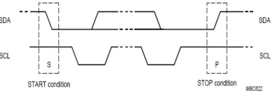
The inter‐integrated circuit bus or more commonly known as I2C is a 2‐wire communication bus developed by Philips in the early 80’s. It is a very simple but effective bus consisting of two lines, a serial data (SDA) and a serial clock line (SCL) which carries information between the devices connected to the bus. I2C supports three different standard speed modes (standard 100kbits/s, fast 400kbits/s and high 3.4Mbit/s) and the lower speed components are not upward compatible. I2C has two different address register, either 7 bits or 12 bits enabling 112 or 1024 devices to be connected to the same bus with each device having its own unique address and can operate as either a transmitter or receiver. A master device initiates a data transfer on the bus and generates the clock signal to permit a transfer. At this time, any device addressed is considered a slave. An example and overview of how a system is built up around I2C can be illustrated in the figure 2.1 below [2.1]. Figure 2.1: an example of a system build round the I2C bus Data is transferred over the I2C bus while the SDA line is stable during the HIGH period of the clock. The HIGH or LOW state of the data line can only change when the clock signal on the SCL line is LOW as illustrated in figure 2.2.
Development of a Multi‐bus platform for automation testbed Master Thesis CEL505 Figure 2.2: shows a valid data transfer on the I2C bus. The start conditions are unique and defined as the following two cases: A HIGH to LOW transition on the SDA line while SCL is HIGH. This situation indicates a START condition. A LOW to HIGH transition on the SDA line while SCL is HIGH defines a STOP condition. An illustration shows the start and stop conditions in figure 2.3.
Figure 2.3: illustrates the valid start and stop conditions on the I2C bus.
The I2C bus protocol has the following appearance (see figure 2.4). Every byte put on the SDA line must be 8 bits long, followed by a acknowledge bit (ACK) generated by the master. During this acknowledgement bit clock pulse the transmitter releases the SDA line which must be pulled down by the receiver in order to confirm the transfer. If the slave does not acknowledge then it leaves the SDA high which gives the master the opportunity to either generate a stop condition or a repeated start command to initiate a new transfer. An illustration of this process can be seen below in figure 2.4. Figure 2.4: A basic I2C protocol appearance. A data transfer is conducted in the following way: After a start condition is initiated, a slave address is sent. This address is seven bits long which is followed by an eight bit which is a data direction bit (Read = 1, Write = 0). When an address is sent, each device in a system compares the first seven bits after the start condition with its address. If they match then the device considers itself addressed as a slave‐
Thereafter data is transferred by the same procedure as described above until the master issues a stop condition. If the master still wishes to communicate with the bus then it can generate a repeated start condition and address another slave address without first generating a stop condition. Various combinations of read and write formats are then possible within such a transfer. An example of a transfer can be seen in figure 2.5. Figure 2.5: an overview of a typical data transfer cycle
2.1.1 Arbitration
The I2C bus was originally developed as a multi‐master bus. This means that more than one device initiating transfers can be active in the system. When using only one master on the bus there is no real risk of corrupted data, with the except of a slave device is malfunctioning or if there is a fault condition involving the SDA / SCL bus lines. This situation changes with 2 MCUs. [2.2]
Assume that one of the MCU's missed the START condition and still assumes that the bus is idle, or that it just started up after a reset and wants to start talking on the bus. This could lead to problems, fortunately, the physical bus setup helps out since the bus structure is a wired AND (if one device pulls a line low it stays low). When a master changes the state of a line to HIGH, it must always check that the line really has gone to HIGH. If it stays low then this is an indication that the bus is occupied and some other device is pulling the line low. Therefore the general rule of thumb is: If a master can’t get a certain line to go HIGH, it lost arbitration and needs to back off and wait until a stop condition is seen before making another attempt to start transmitting. This kind of back‐off condition will only occur if the two levels transmitted by the two masters are not the same. Therefore, let's have a look at the following figure, where two MCUs start transmitting at the same time as shown in figure 2.6. Figure 2.6: An example of arbitration on the I2C bus
The two MCU's are accessing a slave in write mode at address b’1111001’. The slave acknowledges this. So far, both masters are under the impression that they "own" the bus. MCU1 wants to transmit b’01010101 to the slave, while MCU2 wants to transmit b’01100110’ to the slave. The moment the data bits do not match anymore (because what the MCU sends is different than what is present on the bus) one of them loses arbitration and backs off. Obviously, this is the MCU which did not get its data on the bus. For as long as there has been no STOP present on the bus, it won't touch the bus and leave
Development of a Multi‐bus platform for automation testbed Master Thesis CEL505 the SDA and SCL lines alone (yellow zone). The moment a STOP was detected; MCU2 can attempt to transmit again.
From the example above it can be concluded that the master is pulling the line LOW in an arbitration situation that always wins the arbitration. The master which wanted the line to be HIGH when it is being pulled low by the other master loses the bus. This is called a loss of arbitration or a back‐off condition.
2.1.2 Clock synchronization
All masters generate their own clock on the SCL line to transfer messages on the I2C‐bus. Data is only valid during the HIGH period of the clock. A defined clock is therefore needed for the bit‐by‐bit arbitration procedure to take place. [2.1]
Clock synchronization is performed using the wired AND‐gate connection of I2C interfaces to the SCL line. This means that a HIGH to LOW transition on the SCL line will cause the devices concerned to start counting off their LOW period and, once a device clock has gone LOW, it will hold the SCL line in that state until the clock HIGH state is reached. However, the LOW to HIGH transition of this clock may not change the state of the SCL line if another clock is still within its LOW period. The SCL line will therefore be held LOW by the device with the longest LOW period. Devices with shorter LOW periods enter a HIGH wait‐state during this time (see figure 2.7). Figure 2.7: An illustration of clock synchronization When all devices concerned have counted off their LOW period, the clock line will be released and go HIGH. There will then be no difference between the device clocks and the state of the SCL line, and all the devices will start counting their HIGH periods. The first device to complete its HIGH period will again pull the SCL line LOW. In this way, a synchronized SCL clock is generated with its LOW period determined by the device with the longest clock LOW period, and its HIGH period determined by the one with the shortest clock HIGH period.
2.2 The Control Area Network bus
CAN (Controller Area Network) protocol was developed by Robert Bosch, GmbH. CAN is an international standard (ISO 11898) and it was developed for the automotive industry but is now used in many other industrial automation and control applications. CAN is a high‐integrity serial bus system for real‐time control applications and with multi‐master capabilities which means that several CAN nodes can request the bus and all nodes are able to transmit data. The error detecting and error handling mechanism for CAN is sophisticated. The CAN bus can operate up to 1 Mbit/s data this applies on networks up to 40 meters, for longer distance the data rate will be reduced. In figure 2.8 a illustration is shown on how a CAN system can be built. [2.3‐2.4]
bus is to all nodes on the bus and the message does not contain addresses of the transmitting node or the intended receiving nodes instead the message contains a message identifier and it defines content and priority of the message which makes it unique within the whole network. [2.5‐2.8] Figure 2.8: shows how a CAN system is built up The CSMA/CD protocol is when a period of no activity occurs on the bus, every node on the network must monitor the bus for a period before trying to broadcast a message on the bus (Carrier Sense) and every node has equal opportunity to transmit its message on the bus (Multiple Access). When nodes are able to broadcast it can occur that two or more nodes start to broadcast at the same time and the nodes can detect it and take the appropriate action (Collision Detection). Figure 2.9: illustrates how node 3 wins arbitration The CAN protocol utilize a non‐destructive bitwise arbitration method so that a message with higher priority will remain intact and without a delay after arbitration is completed even if collisions are detected (figure 2.9). The node with the highest priority message will be at the end the only transmitter on the bus and the rest of the nodes with lower priority messages will become receiver and wait until the bus becomes available to retransmit its message again. It is important that no two nodes may transmit the same Arbitration Field which determines the priority of the message otherwise the non‐destructive bitwise arbitration method will not succeed, but there is one exception for that rule that is when the message has no data then any node may transmit that message.
2.2.2 CAN messages
The CAN‐bus has four different frames (types of messages), Data Frame, Remote Frame, Error Frame, and the Overload Frame which will be explained later in this chapter. Interframe spacing separates Data Frames and Remote Frames from the previous frames whatever type they are.
Figure 2.10: shows where the Interframe separation is located on the CAN bus
Development of a Multi‐bus platform for automation testbed Master Thesis CEL505 The Interframe spacing consists of a two bit fields: Intermission that is at least three recessive bits and Bus Idle which is a bit field with arbitrary length and for nodes that are in Error Passive Sate has also a bit field called Suspend Transmission (figure 2.10) which is made of eight recessive bits. The intermission allows nodes time for internal processing before the start of the next frame. After the Intermission, the recessive state (Bus Idle) on the bus line continues until the next transmission for Error Active nodes. For Error Passive node after sending a message it sends eight recessive bits (Suspend Mode) following Intermission before starting to send any more messages or recognize the bus line to be idle.
2.2.2.1 Data Frame
The Data Frame (figure 2.11) is the most common message type and it basically consists of: Arbitration Field which determines the priority of the message on the bus it is either 12‐bits or 32‐bits depending on whether Standard Frames or Extended Frames are utilized. The higher priority the lower the Arbitration Field number is. The Arbitration field consists of an identifier (11‐bits or 29‐bits) and of one RTR‐bit (Remote Transmit Request) and if Extended Frames is used then one SRR‐bit (Substitute Remote Request) and one IDE‐bit (Identifier Extension) exists. The IDE‐bit is used to define the messages as an Extended Data Frame and the RTR‐bit is used by a node that request information from another node. Data Field can hold up to eight bytes of data. CRC Field is a 15‐bits checksum which is used for error detection. Acknowledge Field which is used to check that the message received correctly.
Figure 2.11: Data Frame
2.2.2.2 Remote Frame
The Remote Frame (figure 2.12) is just like a Data Frame, but the RTR‐bit is recessive instead of dominant as it is for a Data Frame message, and the Remote Frame do not have a data field. A node that wants to receive information can send a Remote Frame message on the CAN‐bus, and the message can be picked up by another node that responds with a Data Frame with the same Arbitration Field as the Remote Frame had (figure 2.13). The problem with Remote Frame is that the arbitration will not work if the Data Length Code is not set to the length of the expected response message. Figure 2.12: Remote Frame Figure 2.13: example of Remote Frame works
2.2.2.3 Error Frame
The error frame is transmitted when a node detects a fault on the bus to other nodes and they will also transmit error frames. The transmitting nod will try to retransmit the message again automatically. A node is prevented to take all the bandwidth by repeatedly sending Error Frames by elaborate scheme of error counters. Fault Confinement guarantees that bandwidth exits for critical systems because faults will be confined to the faulty nodes and these nodes will be shut down before they can bring down the network. The Error Frame consists of an Error Flag and an Error Delimiter, the Error Flag is 6 bits of same value, and the Error Delimiter is 8 recessive bits. The Error Flag has two forms; an Active Error Flag (figure 2.14) which has all 6 bits dominant, and a Passive Error Flag (figure 2.15) which has all 6 bits recessive unless it is not overwritten by dominant bits from other nodes. The Error Delimiter allows the nodes to restart the communications on the bus cleanly after an error. Figure 2.14: an active Error Frame Figure 2.15: a passive Error Frame The Error Flag depends on the Error state of the node and there are three different error states: Active Error State, Passive Error State, and Bus‐Of Sate (figure 2.16). Initial state of a CAN bus node is Active Error State, when the node is in Active Error State it can take part of the bus communication and when an error has been detected the node sends an Active Error Flag. When the node is in Passive Error State it takes part of the bus communication but it will not actively destroy the bus traffic when it detects an error it sends a Passive Error Flag only. If a node is in a Bus‐Off State it will not transmit anything on the bus. Each node has two counters: Receive Error Counter (REC) and Transmit Error Counter (TEC). There are several rules deciding how the counters are incremented and/or decremented. To simplify, when a transmitting node detects an error then it increment its TEC and receiving nodes increments their REC. The transmitting node increment its counter with 8 and the receiving nodes increments their counter with 1 because it is a good chance that it is the transmitting node that is the faulty node. The counters will be decremented when receiving and/or transmitting a correct message. When one or both counters are above 126 the node will change from Active Error State to Passive Error State and when TEC passes 255 the node will go to Bus‐Of state. To go back to Active Error State from the Bus‐Of the node has to reinitialize without the fault. Figure 2.16: illustrates how the Error Frame works
Development of a Multi‐bus platform for automation testbed Master Thesis CEL505
Five different errors can be detected which will be described after the last message frame which is the Overload Frame described in chapter 2.2.2.4 and depicted in figure 2.17.
2.2.2.4 Overload Frame
The Overload Frame is made of two bit fields Overload Flag that consists of six dominant bits and Overload Delimiter consists of eight recessive bits. An Overload Frame is generated and put out on the network when the receiving node is not ready to receive any additional message due to internal condition of the receiver or if during intermission detection of a dominant bit. Every node may send up to two consecutively Overload Frames. The Overload Frame is identical to an Active Error Frame, and the only difference between these frames is that Overload Frame does not increase the error counters and does not causes a retransmission of a frame. Figure 2.17: shows an Overload Frame
2.2.3 CAN Errors
As described in 2.2.2.3 there are five types of errors that can be detected on the CAN system and they are: CRC Error, Acknowledge Error, Form Error, Bit Error, and Stuff Error. These will be described in detail in the following sections.2.2.3.1 CRC Error
Cyclic Redundancy Check (CRC) is a 15 bit check sum is calculated by the transmitter and it is transmitted in the CRC field (figure 2.18). All nodes receives the messages and do the same calculations to get their own check sum and then compare the check sums received with its own check sum. If the comparison between the check sums does not match each other a CRC‐Error occurs and an Error Frame is generated and after a proper intermission time the original message is retransmitted. Figure 2.18: shows the CRC area on with the checksum is calculated upon
2.2.3.2 Acknowledge Error
The Acknowledge slot in the Acknowledge Field (figure 2.19)is checked if it contains a dominant bit by the transmitting node because the Acknowledge slot was set as a recessive bit. If the transmitter does not find a dominant bit then no node has received the frame correctly and an Acknowledge Error has occurred. An Error Frame is generated and the original message has to be resent after a proper intermission time.
Figure 2.19: shows the ACK Field
2.2.3.3 Form Error
When an illegal bit is detected in a fixed form bit field as CRC Delimiter, Acknowledge Delimiter, End of Frame, or Interframe Space, then there is a form violation and an Error Frame is sent. The original message will be repeated after a proper intermission time. See figure 2.20 below
Figure 2.20: shows us a Form Error in a CAN message
2.2.3.4 Bit Error
The bus is monitored by all nodes, so a transmitting node sends a bit and monitors the bus, if the transmitter detects that the bit that just has been sent differ from the actual bus level then a Bit Error (figure 2.21) occurs and an Error Frame is transmitted and the original message will be retransmitted. An exception when no Bit Error occurs is when the transmitting node is sending a recessive bit during Arbitration Field or during Acknowledge Slot and monitors a dominant bit on the bus because Arbitration Field and Acknowledge Filed must be able to be overwritten by a dominant bit otherwise arbitration and acknowledge functionality will not be achieved. Figure 2.21: illustrates a Bit Error
2.2.3.5 Stuff Error
Non Return to Zero (NRZ) transmission method is used by the CAN protocol and it means that the bit level on the bus is placed the entire bit time. When 5 consecutive bits with the same polarity is sent then a bit with opposite polarity is sent and the receiving nodes will use it for synchronization, but will ignore it for data purpose. If six consecutive bits with the same polarity are detected between the Start of Frame and CRC Delimiter then the bit stuffing rule has been violated and a Stuff Error (figure 2.22) has occurred. An Error Frame is generated and the original message is repeated.
Development of a Multi‐bus platform for automation testbed Master Thesis CEL505
2.3 The Serial Peripheral Interface Bus
The Serial Peripheral Interface bus or SPI as its shortened is the final bus that will be studied in this project. SPI is a serial bus standard established by Motorola and supported in silicon products from various manufacturers. It is a synchronous serial data link that operates in full duplex (signals carrying data go in both directions simultaneously). [2.11]
When comparing the SPI and I2C then both provide good support for communication with slow peripheral devices that are accessed intermittently but SPI is better suited than I2C for applications that are naturally thought of as data streams (as opposed to reading and writing addressed locations in a slave device). An example of a "stream" application is data communication between microprocessors or digital signal processors or a higher rate ADC. [2.11] SPI can achieve significantly higher data rates than I2C. SPI‐compatible interfaces often range into the tens of megahertz (1‐70MHz is a common range). SPI really gains efficiency in applications that take advantage of its duplex capability, such as the communication between a "codec" (coder‐decoder) and a digital signal processor, which consists of simultaneously sending samples in and out. SPI specifies four signals and a connection example in figure 2.23: [2.9] • SCLK — Serial Clock output from master • MOSI/SIMO — Master Output, Slave Input • MISO/SOMI — Master Input, Slave Output • SS — Slave Select, active low, output from master Alternative naming conventions are also widely used: • SCK, CLK — Serial Clock, output from master • SDI, DI, SI — Serial Data In, Data In, Serial In • SDO, DO, SO — Serial Data Out, Data Out, Serial Out • nCS, CS, CSB, nSS, STE — Chip Select, Slave Transmit Enable (active low, output from master) Figure 2.23: A SPI single master and single slave connection example
SPI devices communicate using a master‐slave relationship. Due to its lack of built‐in device addressing, SPI requires more effort and more hardware resources than I2C when more than one slave is involved. But SPI tends to be simpler and more efficient than I2C in point‐to‐point (single master, single slave) applications for the very same reason because the lack of device addressing means less overhead.
2.3.1 Data Transmission
for the de master m During ea • th • th • th • th Not all tra Transmiss the maste significant has been that value the shift r Transmiss the maste Transmiss wishes/ne controller must disr only one s
2.3.2 Mu
If multiple for each s esired chip. I ust wait for ch SPI clock he master se he slave read he slave send he master re ansmissions sions norma er and one in t bit first, w shifted out, e and does so registers are sions may inv er stops togg sions often c eeds. Howev rs or audio c regard the in slave at a timultiple SPI
e slave devic slave. These If a waiting p at least that cycle, a full d ends a bit on ds it from tha ds a bit on th ads it from t require all fo lly involve tw n the slave; t hile shifting , the master omething wi loaded with volve any nu gling its clock consist of 8‐ ver, other w odecs. Every nput clock a me.I slaves
ces exist, the relationships period is req period of tim duplex data the MOSI lin at same line he MISO line that same lin Figu our of these wo shift regi they are con a new least r and slave h ith it, such a h new data an umber of clo k. Normally, i bit words, a word sizes ar y slave on th nd MOSI sig e master ge s are illustra quired (such me before st transmission ne ne ure 2.24: A SPI d operations t isters of som nected in a r significant b have exchan s writing it to nd the proce ck cycles. W it then desel nd a master re also comme bus that ha gnals, and m nerates a se ted in Figure as for analo tarting to iss n occurs: data transfer to be meanin me given wo ring. Data is bit into the s nged register o memory. If ess repeats (s When there is lects the slav r can initiate mon, such a asn't been a ust not driv
eparate slave e 2.25 [2.10] og‐to‐digital ue clock cycl ngful but the rd size, such usually shift same registe r values. The f there is mo see figure 2. no more da ve. e multiple su as 16‐bit wo ctivated usin ve MISO. The
e select sign conversion) les. [2.11] ey do happen h as eight bit ed out with er. After that en each dev ore data to e 24). ata to be tran uch transmiss rds for touc ng its slave s e master mu al (SS1, SS2 then the n. ts, one in the most t register vice takes exchange, nsmitted, sions if it ch screen elect line ust select and SS3)
Developm Some pro configura SPI port o what it re shift regis through S line for ea
2.3.3 SP
SPI does communi offers no SPI. [2.11] Slaves ca higher‐lev needed a ment of a Mu oducts with tion (Figure of each slave eceived durin ster; daisy ch SPI. Such a fe ach slave. [2.PI drawbac
not have an cation proto flow contro ] n be though vel protocol nd only raw ulti‐bus platfo SPI bus ar 2.26), the fi is designed ng the first g haining is of eature only .10]cks
n acknowled ocol, the SPIl. If you need
ht of as inp for master w data are e orm for auto Figure 2.25: A re designed rst slave out to send out group of cloc ften done wi requires a s Figure 2.26 dgement me master has d hardware f ut/output d r‐slave dialog exchanged. A omation test A multi slave SP
to be cap tput being co during the s ck pulses. Th ith shift regi single SS line 6: A Daisy‐chain echanism to s no knowled flow control evices of th g. In some An example bed PI connection
able of bei onnected to second group he whole cha isters to pro e from the m ned SPI bus confirm rec dge of whet
, you might
he master. S applications of this is an
M ng connecte o the second p of clock pu ain acts as a vide a bank master, rathe
ceipt of dat ther a slave need to do s
SPI does not s, a higher‐l n interface t
Master Thesis
ed in a dai slave input, ulses an exac n SPI commu
of inputs or er than a sep
a. In fact, w even exists. something o
t specify a p evel protoc o a simple c
CEL505 isy chain , etc. The ct copy of unication r outputs parate SS without a . SPI also outside of particular ol is not codec. In
• Requires more pins on IC packages than I²C. • No in‐band addressing; out‐of‐band chip select signals are required on shared buses. • No hardware flow control. • No hardware slave acknowledgment (the master could be "talking" to nothing and not know it). • Supports only one master device. • Without a formal standard, validating conformance is not possible. • Only handles short distances compared to RS‐232, RS‐485, or CAN‐bus. [2.10]
Development of a Multi‐bus platform for automation testbed Master Thesis CEL505
3. Predesign circuitry considerations
In this chapter we discuss the electronic parts and peripherals of the circuit boards that we will construct and requirements that Infotiv supervisors have requested.
3.1 Selecting an appropriate operations controller
The primary requirements here are that the operations controller needs to have I2C, SPI and CAN functionality available so the functionality doesn’t have to be programmed from scratch. The secondary is that the software development tools needed to be cheap, if possible free due to budget restrictions. To select the appropriate operations controller we had to investigate what technologies where available and possible to use in this sort of project.
An FPGA would have been the best choice since it has the option to operate parallelism which would enable measurements and control over several communication ports simultaneously and operate several block functions in the FPGA at the same time. There is also the option of having a MPU, thus these require an OS and would be too complicated to implement and use in this project. The final option was to have a microcontroller unit (MCU), as they are widely available at low cost and very easy to program using a variety of different compilers available on the market. The disadvantage with the MCU is of course that they only operate serially. After a discussion with supervisor and acceptance from Infotiv, a decision was made to go with a MCU. Microchip is one of the leading developers and producers of MCU and has a very wide variety of MCU units. A search on the Microchip website revealed that the MCU family PIC18Fxx80 had built in I2C, SPI, CAN and UART, ideal for our purpose and was therefore selected. One problem was thus that the MCU lacked a direct USB port. This could thus be solved by a company FTDI which specializes in IC chips with an UART USB interface. After a search on their website we found that they had several components which could be used in our system.
3.2 Selecting an appropriate ADC
The requirements of the ADC where that it had to have 8 channels, 12‐bit resolution and of course an I2C interface. After a slight search on the internet we found several different ADC which met this requirement. We selected two primary candidates of whom one was the Analog Devices AD7997/AD7998 (same ADC, different specs/settings) and the second the Linear Technologies LTC2309. In table 3.1 below some specifications and selection criterions can be seen of the two ADC’s:
Table 3.1 Difference between the two different ADCs
ADC: AD7997 (10‐bit) AD7998 (12‐bit) LTC2309 (12‐bit)
Max I2C speed ‐0: 400kHz ‐1: 3.4MHz@5V ‐0: 400kHz ‐1: 3.4MHz@5V 400kHz ‐ Num of HW adr per ADC 3 3 9
Uni‐/bipolar Yes/ Yes/ Yes/Yes
Measuring range 0‐5 V ±2.5 V Supply voltage 2,7 – 5,5V 2,7 – 5,5V 4,75 – 5,25 V Conversion time 2µs 2µs 1.3µs Max data rate 79Kbps 79Kbps n/a Sampling rate (Max) 21kSPS@400kHz 21kSPS@400kHz 14kSPS@400kHz
As shown the Analog Device (AD7998) is overall better performance compared to the Linear Technologies (LTC2309) but the AD7998 is difficult to set up when it comes to addresses. The AD7997/AD7998 has only one addressing pin which enables 3 possible addresses per chip, thus you can select four chip types of the ADC (AD7997‐0, ‐1, AD7998‐0, ‐1) which enabled the possibility to connect 10 AD7997/AD7998 to the same I2C bus. The float I2C address b’010 0000’ on the AD7997 and AD7998 is also the same which would lead to address conflicts if connected wrongly. Since the obvious factor is that the AD7997 is only a 10‐bit ADC.
Overall we decided that the performance requirements where not that strict and setting up the Analog Devices ADC would be too complicated, so the LTC ADC was selected due to its simplicity! Simplicity is also a key factor when designing the system.
3.3 Power supply
The power supply source to the system should be an external one and power both the converter and ADC card.
A consideration was taken whether to use the USB as a supply source. USB 2.0 is specified to support a maximum amount of 500mA output current at +5V on a high‐power bus. The problem is that not every USB port on computers is a high‐power bus thus when connecting to a low‐power bus, the USB can only output 100mA which would be (without having made any power consumption measurements) an insufficient amount of current to power the converter card and attached nodes. It’s better to be safe than sorry.
3.4 Selecting ground
Thus not using the USB power supply, we connect the ground plane to the USB ground I/O. The computer has several voltage regulators and transistors which can regulate and produce a pretty solid virtual ground plane. This virtual ground plane will later be used over the entire system, including to the ADC nodes, enabling the end user the possibility to interconnect their measuring objects ground to the systems virtual ground.
3.5 Protection against high voltage peaks
To protect the circuitry from unexpected ESD discharges a suitable protection system should be implemented to the system.
3.6 Diagnostics
To have a visual aid and confirmation whether an I2C bus channel actually is actively transmitting or not on a channel, a requirement of some diagnostic led’s was made.3.7 Bus connectors
For the I2C bus RJ11 connectors where selected. The RJ11 connector and cable are 4‐wire (telephone cables), perfect for our system thus enabling the wires to contain: 5V supply, ground, SCL and SDA. The foremost reason for this is first of all that the system can be easily mechanical connected and set up. The cables are also cheap and widely available and can be cut to appropriate lengths using a special RJ11 clamp with RJ11 modules.Since no connectors where specified by Mälardalen University, simple 2.54mm pins where used. The user can later simply connect their desired connectors to these pins when developing an enclosure for the board. [3.1] [3.2]
Development of a Multi‐bus platform for automation testbed Master Thesis CEL505
Image 3.1: An RJ11 connector with a RJ11 cable
3.8 Schematics and PCB software
To draw the schematics and design the PCB, the software CadSoft Eagle CAD 5.6.0 Light version (freeware) was used. The freeware version limits the PCB design to a dual layer and maximum size of 100x80mm. [3.3]
4. Circuitry components and design
Next step after the theoretical analysis is to focus on the selection of the key electrical components and designing the schematics and board of the system. In the following chapter describes the selected electrical components as well as schematics for the circuits and the final PCB board. We will start of by describing the converter card, followed by the ADC card and finally say a few words about the external peripherals. Since the converter card is more complex than the ADC card the section has been divided into two parts, the first part where the components are described and second part covering the circuitry and interaction between the components is described.4.1 Converter card components
The converter card is built around a couple of key components. The comprehensive system layout is illustrated in the figure below. Afterwards a more detailed description will follow of each of the main components. Figure 4.1 System overview of the converter card4.1.1 Microcontroller – Microchip PIC18F4680
The purpose of the MCU is to act as an interface to the different bus technologies via LabView. It should firstly obtain instructions and data from LabView and convert them into appropriate command instructions and send them out on the different buses. The MCU should also intake data from the different busses, convert it and send it to LabView for further interpretation and processing.
The Microchip PIC18Fxx80 family MCU’s comes in several models, thus the PIC18F4680 model was selected for this task since it comes with more pins (40 ports). These pins can be used for chip enabling on the SPI bus or as an ADC on the converter card if necessary or for future development or expansion of the converter card. As mentioned before the drawback with the PIC18F4680 is that it does not have a direct USB port, only UART hence a USB UART interface would have to be implemented. Here are some other key features of the PIC18F4680. [4.1] • Wide operating voltage range: 2.0V to 5.5V • High current sink/source 25mA/25mA • Single‐Supply 5V In‐Circuit Serial • Programming™ (ICSP™) via two pins. • 10‐bit, up to 11‐channel Analog‐to‐Digital • Converter module (A/D), up to 100 Ksps o Auto‐acquisition capability
Development of a Multi‐bus platform for automation testbed Master Thesis CEL505 o Conversion available during Sleep • Flexible Oscillator Structure: o Four Crystal modes, up to 40 MHz o Internal oscillator block: 8 user selectable frequencies, from 31 kHz to 8 MHz Provides a complete range of clock speeds, o from 31 kHz to 32 MHz when used with PLL • Enhanced CAN (ECAN): o Message bit rates up to 1 Mbps o Automatic remote frame handling o Advanced error management features
4.1.2 USB UART Interface – FTDI FT232
Since the microcontroller lacks a direct USB connection then a UART USB interface was created using the FTDI FT232 chip. The FT232R is a USB to serial UART interface with optional clock generator output. In addition, asynchronous and synchronous bit bang interface modes are available. USB to serial designs using the FT232R have been further simplified by fully integrating the external EEPROM, clock circuit and USB resistors onto the device. The FT232R adds two new functions compared with its predecessors, effectively making it a “3‐in‐1” chip for some application areas. The internally generated clock (6MHz, 12MHz, 24MHz, and 48MHz) can be brought out of the device and used to drive a microcontroller or external logic. Among other key features are e.g.: • 3.3V to 5.25V single supply operation. • Entire USB protocol handled on the chip. No USB specific firmware programming required. • Data transfer rates from 300 baud to 3 Mbaud (RS422, RS485 and RS232) at TTL levels. • 128 byte receive buffer and 256 byte transmit buffer utilising buffer smoothing technology to allow for high data throughput. • Fully integrated clock generation with no external crystal required plus optional clock output selection enabling a glue‐less interface to external MCU or FPGA. • Transmit and receive LED drive signals.
• FTDI’s royalty‐free Virtual Com Port (VCP) and Direct (D2XX) drivers eliminate the
requirement for USB driver development in most cases. [4.2]
4.1.3 I
2C Switch – Texas Instruments PCA9548A
The Texas Instruments PCA9548A has eight bidirectional translating switches that is controlled via the I2C bus. The SCL/SDA upstream pair fans out to eight downstream pairs, or channels. Any individual SC (x)/SD (x) channel or combination of channels can be selected, determined by the contents of the programmable control register. The switch has three addressing pins which can enable the use of up to 8 switches. The switch supports I2C fast mode (400kHz) and has also implemented ESD protection. [4.3]
4.1.4 I
2C Accelerator – Linear Technologies LTC4311
To ensure that the I2C works sufficiently over a longer distance cable, a accelerator was implemented in the system. When sending on the I2C bus with the frequency of 400kHz, the raise time of the signal significantly increases when compared to a regular pull‐up resistor.
The LTC4311 allows multiple device connections or a longer, more capacitive interconnect, without compromising slew rates or bus performance, by using two slew limited pull‐up currents. During positive bus transitions, the LTC4311 provides slew limited pull‐up currents to quickly slew the I2C lines to the bus pull‐up voltage. During negative transitions or steady DC levels, the currents are disabled to improve negative slew rate, and improve low state noise margins. An auto detect standby mode reduces supply current if both SCL and SDA are high. When disabled, the LTC4311 goes into low (<5μA) current shutdown. An illustration of how it works can be seen in the chart 4.1 below. [4.4] Chart 4.1: illustrates how an accelerator works
4.1.5 CAN Transceiver MCP2550
The Microchip MCP2551 is a high‐speed CAN, fault‐tolerant device that serves as the interface between a CAN protocol controller and the physical bus. The MCP2551 provides differential transmit and receive capability for the CAN protocol controller and is fully compatible with the ISO‐11898 standard, including 24V requirements. It will operate at speeds of up to 1 Mb/s. Typically, each node in a CAN system must have a device to convert the digital signals generated by a CAN controller to signals suitable for transmission over the bus cabling (differential output). It also provides a buffer between the CAN controller and the high‐voltage spikes that can be generated on the CAN bus by outside sources (EMI, ESD, electrical transients, etc.).
The MCP2551 CAN outputs will drive a minimum load of 45ohm, allowing a maximum of 112 nodes to be connected (given a minimum differential input resistance of 20kohm and a nominal termination resistor value of 120ohm). [4.5]
4.1.6 Voltage Regulator REG1117-5.0
This is a standard surface mounted Low Drop Out (LDO) voltage regulator (SOT‐233) developed by several electronic component makers. It delivers a maximum output range of 5V/800mA (4VA) which is sufficient to power the key components in the system. The REG1117‐5.0 can handle an input voltage range of about 15V‐6,5V, dependent on manufacture of the REG1117 you select.
This component was chosen because of its wide input voltage range (allowing the users to use a numerous different AC/DC adapters) and high and stable output current allowing the usage of multiple nodes without suffering power‐loss failure due to insufficient VA. [4.6]
4.1.7 TVS Diodes
The Transient Voltage Suppression (TVS) diodes is an electronic component used to protect sensitive electronics from voltage spikes induced on connected wires. The device operates by shunting excess current when the induced voltage exceeds the avalanche breakdown potential. It is a clamping device, suppressing all overvoltage’s above its breakdown voltage. Like all clamping devices, it automaticallyDevelopment of a Multi‐bus platform for automation testbed Master Thesis CEL505 resets when the overvoltage goes away, but absorbs much more of the transient energy internally than a similarly rated crowbar device.
One TVS diode was put on the converter card supply line in case of any unexpected ESD discharges. The diodes that we selected for this circuitry was the bidirectional STMICROELECTRONICS SM6T7V5CA (VBR at 7.5V, 600W). An illustration of the TVS diodes characteristics can be seen in the figure 4.2
below. [3.4‐3.5] Figure 4.2: the characteristics of a TVS diode
4.2 Converter card design
In this section a description will be made of how the components where connected to each other and their setup.4.2.1 Power supply and ground
This power circuit is used to make sure that the supply voltage for the rest of the circuitry is stable at 5V and gives the circuit also a stable ground. The ground is also connected to the USB ground cable and DC jack re‐connector to ensure its stability. A dual pole slide switch acts as on/off toggle for the circuitry. A 7.5V 600W bidirectional TVS diode was connected between 5V and ground to protect the system of any unexpected ESD discharges. All capacitor values were selected from the datasheet. The power supply circuitry is shown in figure 4.3 below. Figure 4.3: shows the regulator schematics (Block R)
4.2.2 Setting up the FTDI circuitry
The FTDI FT232 USB UART chip is connected to the USB via USBDP and USBDM. Even though a built in internal resistors in the FTDI, a 22ohm resistor was put in series with the USB connector to lower the current. The FTDI is connected to the MCU with the TXD, RXD, RTS, CTS, DTR and DSR pins. The TXD and RXD is connected to MCU’s Rx and Tx (UART) while the RTS, CTS, DTR and DSR pins are connected to regular digital IO pins on the MCU which if needed could be set and programmed later on for additional error handling. OSCI and OSCO are connected to the external 12MHz crystal which is both connected to the FTDI and MCU for better synchronization of their operations. The CBUS0 and CBUS1 go low when active, creating a current through the led’s and resistor, indicating that a transmission (CBUS0) or reception (CBUS1) is being conducted over the USB bus. The FTDI setup circuitry is shown in the figure 4.4 below Figure 4.4: FTDI schematics (Block F)4.2.3 Setting up the MCU circuitry
In the MCU, port Rx and Tx are connected to the FTDI (pin 25, 26) while the RD4 to RD7 ports are set in the MCU as digital IOs and connected to the CTS, RTS, DTR and DSR. The MCLR port (pin 1) is connected to a “push button switch” and is used to reset the MCU while the PGD and PGC (pin 39, 40) are connected to a 5x2 pin header which is used with the MikroElektronika PicFlash2 programmer to write the hex‐file to the MCU.
The I2C bus consisting of the CLK and SDA (pin 18, 23) which are connected to the TI PCA9548A I2C Switch together with RC0, RC1 and RC2 (pin 15, 16, 17) which are the address control pins for the switch and the RD1 (pin 20) which finally is the reset control port for the switch.
The SPI uses the SCK, SDI, SDA and SS ports (pin 18, 23, 24, 7) which are the standard set ports of the SPI. Note that thus the SS port (pin 7) is specified to be the chip enable port thus any other digital IO pins on the MCU can be set for that operation.
Note also that the SPI and I2C bus share two ports, the same CLK/SCK and SDA/SDI (pin 18, 23) so when the I2C or SPI bus are running, they come in conflict with each other. Thus this then no addition
Development of a Multi‐bus platform for automation testbed Master Thesis CEL505 circuits come in conflict thus because in the SPI the SS (or any other specified digital IO) must be enabled to run the chip and while using the SPI, the I2C switch can be closed thus not
Finally 8 ports, RA0‐4 and RE0‐2 (pin 2‐6, 7‐9) are connected to an 8x1 pin header which can be programmed and used either used as a digital I/O to perhaps enable or control SPI circuits using a Daisy chain connection (mentioned in chapter 2.3), as a 10‐bit built in ADC or any other optional function programmed by the user. An illustration of the MCU circuitry is shown in figure 4.5 below.
Figure 4.5: The MCU schematics (Block M)
4.2.4 I
2C Switch Setup
The A0, A1, A2 input ports (pin 1, 2, 21) to the switch are both connected from the MCU and from there set to high. This gives the switch the global I2C address: 0xEE. The switch can be reset in the event of a timeout or other improper operation by asserting a low in the RESET input (pin 3). The I2C
input from the MCU is connected to the SCL and SDA ports (pin 22, 23) with pull‐up resistors connected between the MCU and switch on the SPI bus. The remaining I2C ports are bidirectional and each connected to an RJ11 output port and an accelerator. The switch circuitry is illustrated in figure 4.6 below.
Figure4.6: I2C switch schematics (Block S)
4.2.5 I
2C Accelerator setup
The accelerator was connected to the I2C bus as depicted in the figure 4.7 below. One accelerator was connected to each of the eight I2C outputs on the converter card. 10kohm pull up resistors where used with the accelerator. Figure 4.7: Accelerator schematics (Block A)4.2.6 SPI setup
The SPI bus output consists of simple a 6x1 2,54mm header pins with a 10kohm pull‐up resistor connected to the four bus wires (SDI, SDO, SS and CLK). The last two remaining pins are a +5V supply pin and GND and where placed on the outer side of the pin header. The circuitry for the SPI setup is shown in figure 4.8. Figure 4.8: SPI IO port (Block P)
Development of a Multi‐bus platform for automation testbed Master Thesis CEL505
4.2.7 CAN setup
The CAN high and low output where also like the SPI connected to a 4x1 pin header with the outer pins being the supply and ground pins. A 60kohm resistor was connected to the Rs pin giving the transceiver a slew rate of approx 7V/us. Schematics can be seen in figure 4.9
Figure 4.9: CAN schematics (Block C)
4.2.8 Converter card schematics
A comprehensive view of the whole converter card schematics can be seen in figure 4.10 below.