Sigma-Delta Based Techniques For
Future Multi-Standard Wireless Radios
S t e f f e n A l b r e c h t
Stockholm 2005
Laboratory of Electronics and Computer Systems Department of Microelectronics and Information Technology
Royal Institute of Technology, Stockholm, Sweden
Thesis submitted to Royal Institute of Technology in partial fulfilment of the requirements for the degree of Doctor of Technology
Steffen Albrecht
Sigma-Delta Based Techniques For Future Multi-Standard Wireless Radios
ISBN 91-7178-170-6 ISSN 1651-4076
ISRN KTH/IMIT/LECS/AVH-05/07--SE TRITA-IMIT-LECS AVH 05:07
Steffen Albrecht, 2005
Royal Institute of Technology
Department of Microelectronics and Information Technology Laboratory of Electronics and Computer Systems
Isafjordsgatan 39
iii
v
Contents
Abstract vii Acknowledgements ix
Relevant Publications xi
List of Abbreviations xiii
1. Introduction 1
1.1 A Brief History of Communication 1
1.2 Motivation of this work 3
1.3 Wireless Radio Principles & Standards 4
1.3.1 Modulation 4
1.3.2 Access Techniques 9
1.3.3 Wireless Communication Standards 12
1.4 Radio Receiver Architectures 16
2. Sigma-Delta Modulation 23
2.1 The Modulation Principle 23
2.2 Modulator Topologies 27
3. Frequency-Locked Loop 35
3.1 Frequency Synthesizer Concepts 35
3.2 Frequency-Locked Loop 42
3.2.1 Synthesizer Architecture and Principle 42
3.2.2 Detection Process 45
3.2.3 Conversion Process 53
3.2.4 Settling Time Limit 57
3.3 Simulations and Results 61
4. Multi-Standard ADC 69
4.1 Data Converter Introduction 69
4.2 Dual-Standard ADC 71
4.2.1 ADC Performance Specifications 72
4.2.2 Converter Architecture 73
4.2.3 Decimation filter 76
4.3 Simulations Results 77
5. Summary and Conclusion 81
vii
Abstract
Improvements in process technology and design innovations have resulted in com-pact and cost effective digital baseband solutions. The radio part, however, has re-mained a bottleneck in terms of chip area and power consumption as the feature size of analog devices does not directly benefit from scaling. With the addition of yet more standards into emerging products, the requirements of future radios will extend over characteristic performance features into demands of programmable and reconfigurable hardware for radios covering multiple frequency bands. Hence, a guideline in the de-sign of such radios is a large degree of hardware sharing.
The thesis investigates the application of sigma-delta modulation to arising multi-standard wireless radios. First, it reviews principles in wireless radios, such as selected modulation and access techniques. It also examines several communication standards of personal wireless radios as well as common receiver architectures for their imple-mentation. This is followed by general considerations and background information about sigma-delta modulators. In the third and fourth chapter, implementations to two blocks of a wireless radio receiver system are suggested: An architecture for a frequen-cy synthesizer and an implementation of an analog-to-digital converter.
In the first contribution, the thesis develops a novel concept for frequency synthesis that is more suitable for multi-band, multi-standard radio architectures, achieving a large amount of hardware sharing among different wireless standards. As a second pil-lar, the thesis contributes with the design of a dual-standard sigma-delta modulator for data conversion within a radio receiver. Parts of the work concerning the dual-standard modulator are embodied in a granted swedish patent.
ix
Acknowledgements
The studies presented in this thesis would naturally not have been achievable with-out the help of many, both from university and industry. I therefore would like to ex-press my sincere gratitude and thanks to everybody who helped me with advice, discussions and directions in the pursuit of my studies.
In particular, I am thankful to my supervisors Prof. Mohammed Ismail and Prof. Hannu Tenhunen. They gave me the opportunity to carry out the presented studies and provided guidance though instructions and consultation. I very much appreciate their encouragement and advice in the process of the last few years.
Significant additions to my studies also came from outside KTH. Here, I like to mention Prof. Yasuaki Sumi from Tottori Kankyo University in Japan. His expertise and background in the field of frequency synthesizers helped in the conduct of my re-search. I am thankful for the twofold opportunity to visit his department and university for several months as a visiting scholar. Noticeable contribution also came from Michael Wang, with St. Jude Medical AB. His insight and understanding of circuit de-sign and RF background was an important contribution. He helped to find solutions to overcome seemingly unmanageable problems.
I furthermore would like to thank all my colleagues at Royal Institute of Technology who contributed in one or another way with discussion, questions and ideas towards new and different thoughts and perspectives. Representative for them all, I would like to highlight the names of a few in alphabetical order: Jad Atallah, Abhijit Kumar Deb, Xinzhong Duo, Andreas Gothenberg, Jinliang Huang, René Krenz, Bingxin Li, Wim Michielsen, Costantino Pala, Dinesh Pamunuwa, Delia Rodríguez de Llera González, Ana Rusu, Saúl Rodríguez, Adam Strak, Yiran Sun, Nil Tarim, and Li-Rong Zheng.
Undoubtedly, I am indebted to my family and friends for their continued support and for their sacrifice due to my absence from home throughout the years of my stud-ies. And last, but not least, I would like to thank the Swedish Foundation for Strategic Research (SSF) for funding my studies.
xi
Relevant Publications
[1] Steffen Albrecht, Adam Strak, Yasuaki Sumi and Mohammed Ismail; "Fre-quency Detector Analysis for a Wireless LAN Fre"Fre-quency Synthesizer"; IEEJ Analog International VLSI Workshop, Macao; 2004
[2] Steffen Albrecht, "A Frequency-Locked Loop Using Sigma-Delta Modula-tion", Conference for Design Automation & Test in Europe (DAC), Ph.D.-Forum, Germany; 2003
[3] Steffen Albrecht, Yasuaki Sumi, Mohammed Ismail, and Hannu Tenhunen, "A Frequency Synthesizer Using Frequency Difference Detection", 46th IEEE Midwest Symposium on Circuits and Systems, Cairo, Egypt; 2003
[4] Steffen Albrecht, and Hannu Tenhunen, "A Frequency Synthesizer Architec-ture for RF Applications", Proceedings of Norchip conference, Riga, Latvia; 2003
[5] Steffen Albrecht, Andreas Gothenberg, Yasuaki Sumi, and Hannu Tenhunen, "A Study of Nonlinearities For a Frequency-Locked Loop Principle", South-West Symposium for Mixed Signal Design (SSMSD), Las Vegas, USA; 2003
[6] Steffen Albrecht, Yasuaki Sumi and Hannu Tenhunen, "A Frequency Synthe-sizer Principle with Sigma-Delta Loop Filtering", IEEJ International Analog VLSI Workshop, Singapore; 2002
[7] Steffen Albrecht et al., "A Dual-Standard GSM/DECT Baseband Sigma-Delta ADC", NorChip conference, Turku, Finland; 2000
[8] Steffen Albrecht et al., "A Front-End Receiver Sigma-Delta Modulator", Swedish Patent SE0002065-1, Stockholm; 2000
[9] Steffen Albrecht, Xiaopeng Li, Bingxin Li, Costantino Pala, Yonghong Gao, Mohammed Ismail and Hannu Tenhunen, "A Sigma-Delta A/D Based Archi-tecture for Multi-Standard Front-End Radio Receivers", IEEJ International Analog VLSI Workshop, Stockholm, Sweden; 2000
xiii
List of Abbreviations
AC Alternating Current
ADC Analogue-to-Digital Converter
AM Amplitude Modulation
AMPS Advanced Mobile Phone Service
ASK Amplitude Shift Keying
BPSK Binary Phase Shift Keying
CCK Complementary Code Keying
CDMA Code Division Multiple Access
CT Continuous Time
DAC Digital-to-Analog Converter
DC Direct Current
DECT Digital Enhanced Cordless Telecommunications
DNL Differential Nonlinearity
DR Dynamic Range
DSP Digital Signal Processor
DT Discrete Time
EDGE Enhanced Data for Global Evolution
ETSI European Telecommunications Standards Institute
F Noise Factor
FCC Federal Communications Commission
FDMA Frequency Division Multiple Access
fFB frequency of feedback signal
FHSS Frequency Hopping Spread Spectrum
FM Frequency Modulation
fs sampling frequency
FS Frequency Synthesizer
FSK Frequency Shift Keying
GFSK Gaussian Frequency Shift Keying
GMSK Gaussian minimum Shift Keying
GSM Global System for Mobile communication
IF Intermediate Frequency
IMT-2000 International Mobile Communications at 2000 MHz
INL Integral Nonlinearity
ISM Industrial, Scientific and Medical (frequency band)
ITU International Telecommunication Union
MASH Multi-stAge noise SHaping
NF Noise Figure
NMT Nordic Mobile Telephone
NTF Noise Transfer Function
OFDM Orthogonal Frequency Division Multiple access
OSR OverSampling Ratio
OTA Operational Transconductance Amplifier
PA Power Amplifier
PDC Personal Digital Cellular
PHS Personal Handyphone System
PM Phase Modulation
PSK Phase Shift Keying
QAM Quadrature Amplitude Modulation
QPSK Quaternary Phase Shift Keying
RF Radio Frequency
xv
Σ∆ Sigma-Delta
SC Switched Capacitor
SNDR Signal-to-Noise plus Distortion Ratio
SNR Signal-to-Noise Ratio
SOI Silicon On Insulator
SQNR Signal-to-Quantization Noise Ratio
STF Signal Transfer Function
TACS Total Access Communication System
TDMA Time Division Multiple Access
UMTS Universal Mobile Telecommunications System
WCDMA Wideband Code Division Multiple Access
1. Introduction
This chapter will first give a brief historical review on wireless communications and mention the motivation for this work. Then, principles of selected modulation and access techniques em-ployed in today’s radio communication are examined. The impact of modulation schemes on the requirements of utilized hardware is viewed upon. Secondly, several communication standards are compared with respect to application area and performance parameters. The third section describes radio architectures, typically found in today’s radio communication.
1.1 A Brief History of Communication
Before stepping into principles and standards of radio communication, this section will glance over a few important milestones in the development of information trans-mission. This review is of course by no means complete, as this is not the scope of this thesis, nor is it intended to be encyclopaedically. Maythe inventors of past and present excuse, if they have been left out here.
Today’s accessibility of communication around the globe using telephones, fax, ra-dio and television, internet connections, mobile phones at relatively low costs is a mat-ter of course. However, this development has been a long process. Transmission of information, i.e. the desired data, over distance to a receiving instance has always played a large role in human life. Without it, human interaction and coordination or im-parting of knowledge would not have be possible. Before an automated procedure for a transmission was invented, messages had to be carried from a sender to the destina-tion: Afoot or mounted, oral or written, crypted or plain; using letters, smoke, trumpets or flags. Limits in number of symbols, transmission distance and speed made these transmissions time consuming or complicated.
In the beginning of the 18th century, during the French revolution, Claude Chappe, a former priest, built a mechanical-optical communication device, a so called sema-phore telegraph (figure 1.1). It was first used in 1794 and consisted of 15 repeating sta-tions in a line of sight, linking the cities Lille and Paris [Chapp1794]. The distance of about 200 km could be covered in a few minutes what used to be many hours for a mounted courier. A technology that proved critical for an aspiring France. Other tele-graph systems had also been tested before, but Chappe was presumably the first who constructed an applicable and mechanical, wireless communication system.
The invention of the galvanometer by Johann Schweigger and the work on electro-magnetism by people like Hans Christian Oerstedt, André Marie Ampère, William Sturgon andMichael Faraday in the 1820’s laid the basics for Joseph Henry’s principle of telegraphing [Henry1831]. This principle was later used in the development of a long distance telegraph communication system like the ones by Wheatstone and Cooke [Wheat1837] and by Samuel F.B. Morse [Morse1840]. In 1876, Elisha Gray and Al-exander Graham Bell developed a device that transmitted speech electrically [Bell1876]; the telephone was invented. Although communication was bound to wires, both telephone and telegraph provided fast and reliable means of communication of both text and sounds, and their technological successors are still in use today.
The physicist Heinrich Rudolf Hertz extended Maxwells ideas on electromagnetic waves. He proved the physical existence of radio waves experimentally [Hertz1892]. The path was open for the wireless telegraph and the radio. Physicist Nikola Tesla is credited with the invention of modern radio [Tesla1897]. He obtained more than 100 patents in the areas of motors/generators, transformers, lightning, radio, engines and other areas. In the dawn of a new century, Guglielmo Marconi, an italian inventor, built a first practical radio communication link in England [Marco1900]. The first transat-lantic wireless transmission of Morse code followed in 1901. With the development of the audion tube by De’Forest [DeFor1906], radio waves could be amplified, which en-abled the advance of wireless telephony. Military and enterprise interests pushed for improvements in radio communications. Commercial radio and first television broad-casting started in the 1920’s, radar detection was fit for service in 1936. With the in-vention of the transistor by Shockley, Brattain and Bardeen in 1947 and the advance into integrated circuits, [Kilby1959] and [Noyce1959], the area of smaller, lighter and more powerful radios began. Mobile, hand held terminals became available and
Motivation of this work 3
lar radio communication systems were developed. The first commercial cellular phone system was in operation in Tokyo in 1979.
1.2 Motivation of this work
With communication technology developing in different parts of the world and driv-en by differdriv-ent economic interests, naturally, a large variety of communication meth-ods matured. Today’s frequency spectrum is crowded by a large number of applications. The same method might occupy different bands in different countries. With numerous standards defined for wireless communication, the need for interoper-ability between various technologies arises. Mobile terminals such as phones, PDAs or notebooks gain seamless access to a multitude of available services. This in turn reduc-es the number of devicreduc-es and increasreduc-es user-friendlinreduc-ess. But interoperability comreduc-es at the expense of added complexity. Powerful signal processing is accomplished using programmable DSPs. However, radio interface specifications vary considerably and transceiver hardware is typically optimised for a specific standard.
An evolutionary trend for transceivers is therefore not only towards higher data rates. Also integration of several radio interfaces into one programmable and reconfig-urable hardware supporting multiple standards and multiple frequency bands becomes important. Although accommodating several individual, optimised transceivers into one terminal already enables multi-standard operation, it would cause larger imple-mentation costs, higher power consumption and bulkier terminal size.
Due to advances in manufacturing, feature size, speed and area usage of integrated structures improve continuously. An estimation for this development was first given by Gorden Moore in [Moore1965]. The advance of recent processes can be followed from the International Technology Roadmap for Semiconductors [ITRS04] or relevant internet publications from manufacturing companies. However, the mentioned im-provements mainly benefit digital processing. Area, size and power reduction of ana-log circuits is limited by different noise sources.
The work presented in this thesis targets the above mentioned objective of increased flexibility to reduce implementation costs and to add functionality. Multi-standard and multi-band operation is achieved by making use of digital processing and configura-bility.
1.3 Wireless Radio Principles & Standards
A wireless transmission does not necessarily have to be a radio connection. For in-stance, Chappes telegraph system [Chapp1794] used a combination of optical and me-chanical means, a connection without wires. Also, capacitive or inductive crosstalk is a wireless connection, but does not constitute radio communication. For the scope of this thesis, radio communication is referred to as the transmission, emission and recep-tion of informarecep-tion (signs, symbols, images, sound or data) by means of modulated electromagnetic waves. A generalized block diagram of a wireless radio communica-tion system is shown in figure 1.2. Informacommunica-tion from the source, e.g. a baseband signal, is modulated with and frequency translated onto electromagnetic carrier waves in the transmitter prior to emission from an antenna. These waves travel through the channel medium and are then received at another antenna. The receiver detects and demodu-lates the information before handing it over to its destination. During transmission, propagation loss, multipath fading, delay differences and interferences from other communications affect the quality of the signal depending on the used frequency band and the application environment. More details on disturbances of radio communication channels can be found in e.g. [Rappa1996].
1.3.1 Modulation
Modulation and demodulation are essential functions in wireless radio communica-tion systems. Modulacommunica-tion improves transmission, recepcommunica-tion and deteccommunica-tion properties in the presence of noise within the transmission channel. It also adds to security of data transmission. Important attributes of modulation and demodulation are signal trans-mission quality, spectral efficiency and power efficiency. Local and international au-thorities regulate and limit frequency bands for communication. Hence, the same application might occupy different bands in other countries, i.e. requiring a different carrier signal. Different communication standards employ different modulation
tech-Transmitter
Source Receiver Destination
Figure 1.2: Block diagram of a general radio communication system.
Wireless Radio Principles & Standards 5
niques, for reasons of required bit rate, application area or noise impact to the air inter-face.
The transmission quality can be quantified with parameters like Signal-to-Noise Ra-tio (SNR) for analog or audible applicaRa-tions, or with the Bit Error Rate (BER) for dig-ital and data transmission. SNR expresses the ratio of signal power to noise power that is present during communication. The BER, on the other hand, states the ratio of bits that were received erroneously to the total number of transmitted bits within a certain time frame. Hence, it is a measure of how many bits have to be resent to complete the information transfer. A higher transmission quality allows to lower the transmission energy for the same distance and increases battery life. Alternatively, the signals could be transferred over larger distances. Spectral efficiency expresses the ratio of channel throughput to the required radio spectrum. More complex modulation techniques com-bine several bits into symbols that are transmitted within the same or a smaller spec-trum. If the amplitude envelope of a signal becomes variable due to modulation, then the power amplifier (PA) needs to provide amplification with higher linearity. Other-wise, the signal will experience spectral regrowth, causing lower spectral efficiency and energy leakage into adjacent channels [Morai1980], [Sevic1996]. However, highly linear PAs have considerably lower power efficiency. Hence, modulation scheme re-quirements for spectral efficiency and power efficiency have to be traded off.
The basis of modulation is the variation of a carrier by a baseband signal. This car-rier, e.g. a sinusoid, can be modulated by both, amplitude and phase. This converts the baseband signal to the passband. A passband signal can be described as
(1.1) where ωc is the carrier frequency and a(t) and φ(t) are the amplitude and phase of the carrier signal, that vary proportionally with the baseband signal. In analog modu-lation, the carrier is modulated by an analog baseband signal. When varying a(t), φ(t), or dφ/dt, the scheme is called amplitude (AM), phase (PM), or frequency modulation (FM), respectively. AM is more susceptible to noise and interferences and requires lin-ear power amplifiers. PM and FM carry the baseband information in the phase or fre-quency instead. Hence, the carrier envelope is constant, leading to lower linearity requirements for the PA.
Modern modulation schemes employ digital baseband signals for carrier alteration. Digital modulation offers higher resilience to noise or multi-path effects, increases quality of communication and spectral efficiency, and brings better compatibility with digital services. Data security is improved and modern, powerful digital signal proces-sors (DSPs) can be employed for complex modulation schemes. Similar to analog
modulation, the schemes are called Amplitude Shift Keying (ASK), Phase Shift Key-ing (PSK) and Frequency Shift KeyKey-ing (FSK). Their principles are depicted in figure 1.3(a-c) for the case of binary modulation. A general expression of the digital baseband signal x
bb(t) is
(1.2)
with bn being the bit values and Π(t-nTb) the pulse function of interval Tb. The number of discrete values of bn defines the levels of modulation, for instance [-1, 1] or [0, 1] for binary modulation. Each digitally modulated waveform x(t) can be expressed as a linear combination of basis functions:
(1.3) where the Ψj are the orthogonal basis functions and the α
j are their parameters that
were modified by xbb(t), respectively. For m = {1, 2, 3}, the symbols of x(t) in equa-tion (1.3) can be represented graphically. Such representaequa-tions are called signal con-stellations. The larger the geometrical distance between the symbols, the lower the probability of detecting a wrong symbol.
ASK encodes information in the amplitude of one carrier. In binary signalling, the carrier can simply be switched either on or off. ASK offers low circuit complexity, but suffers from signal quality loss due to higher sensitivity to amplitude noise during transmission than PSK and FSK. It is therefore not often used in digital radio commu-nications [Razav1998]. Since there is only one basis function, Ψ1, the signal constel-lation is one dimensional, as shown in figure 1.4a. The modulated signal x(t) of equation (1.3) is described with α1= {0, Ac} and Ψ1= cos(ωct), with Ac being the
car-xbb t( ) bnΠ(t–nTb) n
∑
= x t( ) = α1⋅Ψ1+α2⋅Ψ2+… α+ m⋅Ψm t t t a) ASK b) BPSK c) BFSKFigure 1.3: (a) Amplitude, (b) Phase, and (c) Frequency shift keying for modulation with binary base band signals (shown above)
Wireless Radio Principles & Standards 7
rier amplitude and ωc the carrier frequency, respectively. Phase and frequency shift mechanisms are much less susceptible to amplitude variations, and are hence most of-ten used for wireless radio transmission. In PSK, information is coded in the phase of the carrier. Figure 1.3b and figure 1.4b show the time domain diagram and signal con-stellation for the binary case, i.e. BPSK. The modulated signal x(t) can be described with x(t) = Ac·cos(ωct +φ), where the phase φ can take the values 0 or 180 degree. The constellation now comprises a single carrier, Ψ1= cos(ωct ), and two amplitudes
α1= {-Ac, Ac}. The symbol distance is now twice as large as for binary ASK, which
means lower detection error probability. When using coherent detection, phase syn-chronisation is required between the received carrier and the receiver oscillator.
In frequency shift keying, different symbols are encrypted with frequencies. This principle is illustrated in figure 1.3c. In binary FSK (BFSK), the baseband signal se-lects one of two carriers with equal amplitudes. Hence, the signal x(t) has two basis functions: Ψ1= cos(ωc1t) and Ψ2= cos(ωc2t). The two carrier frequencies are ωc1 and
ωc2, and [α1α2] = {[0 Ac], [Ac 0]} are the amplitude values. The constellation of BFSK is shown in figure 1.4c. It can be seen that the symbol distance is reduced by a factor of √2 with respect to BPSK. Hence, the probability of detecting a symbol erro-neously is increased. Also in frequency shift keying modulation, phase synchroniza-tion is required if coherent detecsynchroniza-tion is used. Despite the higher error probability, BFSK enables simpler detection schemes and better power efficiency [Razav1998].
In binary modulation, one symbol representing a binary value is modulated onto one carrier signal. Higher data rates can be obtained by multiplexing more symbols onto a single carrier. For instance, pairs of two bits [b0 b1] = {[00], [01], [10], [11]} can be mapped to one out of four symbols, say [a b c d]. This requires x(t) of equation (1.3) to have two basis functions, Ψ1 and Ψ2, that are orthogonal with respect to each other. Such modulation scheme is called quadrature modulation. If the phase of the basis sig-nals is modulated, the scheme is called quadrature phase shift keying (QPSK). Equa-tion (1.3) becomes x(t) =α1·cos(ωct) +α2·sin(ωct), with [α1α2] = [±Ac ±Ac]. As two bits comprise one new symbol, the symbol rate is half the bit data rate. Hence, the re-quired bandwidth for the same data stream is reduced by a factor of two with respect to BPSK. Alternatively, twice as much data could be send. The signal constellation for QPSK is shown in figure 1.4d. Variations of quadrature modulation are for instance offset-QPSK (O-QPSK), π/4-QPSK and Mean Shift Keying (MSK). These techniques introduce time offsets, phase rotation, or smooth phase transitions to improve spectral or power efficiency. The higher data rate of QPSK comes at the expense of higher de-tection complexity.
The signal amplitudes in PSK modulation schemes are constant. A combination of phase shifts and amplitude variations allows for a higher level of modulation, for
in-stance in Quadrature Amplitude Modulation (QAM). Each out of M possible symbols represents m bits, with m = log2(M). When modulated with QAM, the signal of equa-tion (1.3) becomes x(t) =α1·cos(ωct) +α2·sin(ωct), where α1= [±A1,…, ±Ak] and
α2= [±A1,…, ±Ak] are the k amplitudes of each basis function.
The constellation of 16-QAM is shown in figure 1.4e. The modulation accuracy and quality of the transmitted QAM signal can be expressed with the error vector magni-tude (EVM). EVM represents the vector distance between ideal and measured symbol in a QAM constellation. As with the techniques mentioned above, more symbols give higher data rates, and hence, better spectral efficiency. But it also increases amplitude and phase noise performance requirements of the (de)modulating circuitry. Increased symbol energy can only partly improve transmission quality, as regulations on maxi-mum transmit power limit this option. Therefore, power and bandwidth efficiency need to be traded off. More detailed discussions on digital modulation schemes can be found e.g. in [Couch1993], [Feher1995], [Proak1989], and [Rappa1996].
Ψ1 0 Αc Ψ1 0 Αc Ψ2 Αc Ψ1 0 +Αc −Αc Ψ1 Ψ2 Αc −Αc −Αc Αc a) ASK b) BPSK c) BFSK d) QPSK Ψ1 Ψ2 e) 16-QAM 0000 0001 0010 0010 0110 0111 0101 0100 1100 1101 1111 1110 1010 1011 1001 1000 Figure 1.4: Signal constellation for (a) ASK; (b) BPSK; (c) BFSK; (d) QPSK; and (e) 16-QAM. The digital numerals represent the modulated symbols.
00 01 11 10 0 1 0 1 1 0 Α1 Α2 −Α2 −Α1 −Α1 −Α2 Α1 Α2
Wireless Radio Principles & Standards 9
Coherent detection requires phase synchronization between transmitter and receiv-er. This phase information is usually obtained from training sequences carried in pilot signals. However, in the presence of strong interferences and low signal levels, phase recovery becomes difficult. Alternatively, noncoherent detection schemes can be em-ployed. For instance, differential phase shift keying (DPSK) does not require phase alignments, as information lies within the phase change from one symbol relative to the previous one, not in absolute phase values. Only an extra starting bit prior to the first transmitted symbol is required for correct interpretation of the symbol sequence. Symbols modulated with noncoherent FSK are detected with bandpass filters (to de-termine if the wanted frequency component is present) and envelope detectors instead of correlation filters. The error performance of noncoherent modulation is slightly worse than for coherent systems. However, reduced complexity and robustness to in-terference make these modulation schemes attractive [Burr1992], [Colav1999], [Razav1998].
1.3.2 Access Techniques
Access techniques regulate the management of available communication channels and allocate connections to the users. Multiple access techniques permit that many us-ers simultaneously access the same fixed bandwidth. A selection of methods employed in todays radio communications are described here.
In Time Division Multiple Access (TDMA), a time frame is split into several frac-tions, so called slots [figure 1.5(a)]. Signals are transmitted for the duration of one time slot within the frame. Hence, the number of physical channels corresponds to the number of time slots. Different users can be assigned to these slots which makes it
pos-Frequency Time Carrier bandwidth 1 2 3 4 m m-1 .. . Communication duration fc
Figure 1.5: Channel definitions for (a) TDMA for n channels, and (b) FDMA for m channels
(a) (b) Frequency Time Frame B a nd w idt h Slot 1 2 3 4 ... n 1 2 3 4 ... n
sible to transmit signals from several users within one time frame. The data is buffered and transmitted at a high rate. Each time slot uses the whole assigned frequency band. The receiver decompresses the signal to its original timing schedule, so that its output is a seemingly continuous stream. Due to buffering and synchronisation, TDMA can-not send analog data directly and is used only for digital communication.
In Frequency Division Multiple Access (FDMA), the available spectrum is divided into several narrower bands [figure 1.5(b)]. A physical channel is now such narrow band, e.g. 30 kHz, with a carrier frequency, fc, at the channel centre. The transmission is continuous, i.e. is suitable for analog signals. Each user is assigned to one carrier for receiving and for transmission to achieve simultaneous access. Hence, the number of signals that can be transmitted corresponds to the number of carriers, and no additional synchronisation data is needed. To increase the number of users, the available spec-trum can be divided into more, narrower bands. However, the modulation technique defines the minimum carrier spacing. In a hybrid FDMA/TDMA system, both access methods are combined. For each carrier with its bandwidth, the time frame is separated into several slots. A physical channel corresponds to a time slot within one carrier.
Code Division Multiple Access (CDMA) is a technique where many users use the whole assigned spectrum and transmit simultaneously. Two different techniques to spread the bandwidth of the original data signal are used. In Direct Sequence Spread Spectrum, DSSS or DS-CDMA, each data signal is assigned a pseudo random noise code (thereof the name ‘code’ division). This canalization or spreading code is a se-quence of binary symbols (chips) and each code corresponds to a physical channel. For each successive connection, the spreading code changes. The required bandwidth for transmission is much larger than the bandwidth of the original signal. To send one bit of information, e.g. a “1”, the whole code sequence is sent. To send a “0”, the comple-ment of the code is sent. After spreading, the signal is modulated to the RF band. Since
Time 1 1 1 1 1 1 5 5 5 5 5 5 2 2 2 2 2 2 3 3 3 3 3 3 4 4 4 4 4 4 6 6 6 6 6 6 Frequency Channel 6 Channel 5 Channel 4 Channel 3 Channel 2 Channel 1 Sub-carrier bandwidth
Figure 1.6: Channel definitions for spread spectrum applications: (a) DSSS, and (b) FHSS
(a) (b)
Time Spreading Codes
Wireless Radio Principles & Standards 11
the signal is coded, the receiver cannot distinguish certain time slots or carriers. The receiver input contains small parts of all signals at each instant of time. The received signal is first down-converted from RF before it is recovered by correlation with the same spreading code as in the transmitter. A second technique used to spread the data bandwidth is Frequency Hopping Spread Spectrum, FHSS or FH-CDMA. The RF spectrum is divided into a larger number of sub-carriers and the transmitted signal switches rapidly between different carriers in a predetermined, pseudo random se-quence. The receiver has to know beforehand where to find the signal at any given time. To cause interference, another transmitter has to send at the same time at the same sub-carrier. The channel definitions are depicted in figure 1.6.
CDMA offers a high immunity to interferences during transmission because the sig-nal energy is spread over a large bandwidth. The effect of band spreading is depicted in figure 1.7. The larger the processing gain, i.e. the ratio of the spread bandwidth to the original data bandwidth, the higher the interference immunity. Longer spreading codes increase the processing gain and improve the system transmission rate. If too many signals are sent out simultaneously by different stations, the bit error rate increas-es due to intersymbol interference. Hence, the channel capacity in DS-CDMA is de-fined as the highest number of codes that are used simultaneously while keeping a defined bit error rate of the receiver.
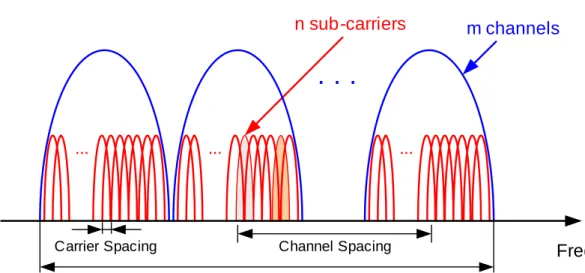
Orthogonal Frequency Division Multiplexing (OFDM) resembles FDMA, but pro-vides several sub-carriers for each channel in the band [figure 1.8]. The sub-carriers are orthogonal to one another, so they can be placed close together in the band without causing interference. A high data rate bit stream is converted into n parallel low rate bit streams. Each parallel bit stream is then modulated on a sub-carrier, where each car-rier modulation can be different (BPSK, QPSK or QAM). To get a higher bandwidth
Figure 1.7: CDMA spectra: (a) original data, (b) spread spectrum after modulation with PN code, (c) received spectrum containing noise and interference, and (d) de-spread signal.
a b c d
Transmitter Receiver
. . .
. . .
efficiency, the sub-carriers are overlapping. The symbol rate in each carrier is low, so intersymbol interference occurs only for large delay spreads. This gives higher toler-ance to multipath delay spread and fading. However, challenges of OFDM are for in-stance sensitivity to frequency offsets, oscillator phase noise and the more complicated design of (de)modulation circuitry.
1.3.3 Wireless Communication Standards
For any wireless communication to function, both transmitter and receiver shown in figure 1.2 have to comply to the same frequency band, method of modulation, and ac-cess technique. For this reason, communication standards are defined. The standards mentioned below represent only a small selection of the range of existing radio com-munication systems.
Since the spectra for wireless services are limited, frequency resources have to be shared to ensure service to a large number of customers. Here, radio communication lends a principle from radio and TV broadcast. If two senders are positioned at a suf-ficiently long distance from each other, their signals have only negligible interference. Hence, they can use the same frequency band for transmission. This frequency reuse principle is commonly extended into a cellular system, as depicted in figure 1.9 for the example with 7 adjacent cells. Each neighbouring cell operates in a different frequency band. Users within a cell are served by one base station until leaving the cell. Then, communication is handed off to the nearest base station with the help of a mobile tel-ephone switching office (MTSO).
. . .
Frequency m channels n sub-carriers ... ... ... Channel Spacing Carrier Spacing Communication BandWireless Radio Principles & Standards 13
Technologies that make extensive use of this cellular approach are for instance per-sonal wireless phone systems. Though already available in the 1940’s, technical and administrative restrictions delayed its advance until the late 1970’s and early 1980’s. Today termed as analog, or first generation wireless telephone, systems like the scan-dinavian Nordic Mobile Telephone (NMT) and the german C-Netz commenced oper-ation in 1981.
Also, the Advanced Mobile Phone Service (AMPS) and Total Access Communica-tion System (TACS) were operaCommunica-tional in 1983 and 1985, respectively. Second genera-tion systems employing digital modulagenera-tion schemes offered increased data rates, better quality and new types of communication. The Global System for Mobile communica-tion (GSM) became a unified standard for Europe and many other countries. Corre-sponding systems in the US are based on standards IS-54/IS-136 and IS-95. In either case, the number of subscribers quickly exceeded channel capabilities, so that addi-tional frequency bands were needed. Whereas first generation systems allowed roam-ing only on a national or bilateral basis, communication standards are largely unified for second generation on a more continental basis. However, roaming with one device on different continents requires multiple transceiver interfaces to be included in the mobile terminal, increasing costs and weight. Wireless communication of the third generation aims for wider roaming services as well as new applications due to higher data rates and more effective use of the available spectrum. Besides improved voice communication, third generation services include transmission of data, video, and in-ternet access, all at reduced costs for subscribers. The standard International Mobile Telecommunications-2000 (IMT-2000) comprises several individual standards, e.g.
MTSO
4
1
2
6
7
53
Universal Mobile Telecommunication System (UMTS), CDMA2000, Enhanced Data rate for Global Evolution (EDGE), and Digital Enhanced Cordless Telecommunica-tions (DECT). Though IMT-2000 greatly improves roaming capabilities, there is yet no single worldwide standard.
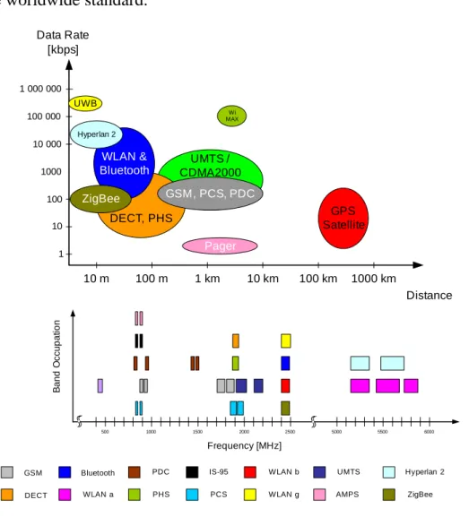
Whereas wireless phone systems aim for long distance connections with relatively low data rate, other applications like wireless local area network (WLAN) services, Ul-tra Wide Band (UWB) or HiperLan target Ul-transmission of large amount of data over shorter distances. Additionally, short distance, low data rate applications for very low costs (e.g. ZigBee) and large data rate, long distance (e.g. WiMAX) systems are avail-able. Figure 1.10 shows an overview of selected standards with relevant data rates ver-sus applicable cell sizes as well as their band occupation. Table 1 compares access
UMTS / CDMA2000 DECT, PHS Data Rate [kbps] Distance WLAN & Bluetooth GSM, PCS, PDC 10 1 100 10 000 1000 100 000 1 000 000 10 m 100 m 1 km 10 km 100 km 1000 km ZigBee UWB Pager GPS Satellite Wi MAX Hyperlan 2 Frequency [MHz] 500 1000 1500 2000 2500 5000 5500 6000 B and O c c u p a ti o n PDC PHS DECT GSM Bluetooth WLAN a WLAN b WLAN g Hyperlan 2 ZigBee UMTS IS-95 PCS AMPS
Figure 1.10: (a) Data rate versus cell size for selected wireless standards; (b) Band occupation for selected standards of Table .
(a)
Wireless Radio Principles & Standards 15
technologies, modulation schemes and other parameters of radio interfaces for various mobile communication standards.
Table 1: Overview for selected mobile communication standardsa
a. References: [IEEE1999a], [IEEE1999b], [IEEE2003a], [IEEE2003b], [IEEE2003c], [Holma2001], [ETSI2001], [MBOA2004], [Goodm1997]
Standard
Frequency Bands
(MHz)b
b. The lower bands correspond to uplink, higher bands to downlink connections.
Data Rate
(air interface) Access Modulation
No. of Channels No. of Carriers Spacing AMPS 824 - 849 869 - 894 10 kbps FDD FM 1 832 30 kHz PCS (IS-54 / IS-136) 824 - 849 869 - 894 1850-1910 1930-1990 48 kbps TDMA/ FDD DQPSK 3 832 30 kHz IS-95 824-849 869-894 1.2288 Mbps DS-CDMA QPSK, O-QPSK 256 1 1.25 MHz GSM 890-915 935-960 1710-1785 1805-1880 270 kbps FDMA/TDMA FDD GMSK 8 124 200 kHz PDC 810-826 940-956 1429-1453 1477-1501 42 kbps TDMA DQPSK 3 640 25 kHz DECT 1880-1930 1.152 Mbps TDMA/TDD GFSK 12 10 1.728 MHz PHS 1895-1918.1 384 kbps TDMA/TDD DQPSK 4 77 300 kHz Bluetooth 2400-2483.5 1 Mbps FH-CDMA TDD GFSK 79 79 1 MHz UMTS/WCDMAc
c. Spectrum according to IMT-2000, including bands for satellite, licensed and nonlicended bands. 1900 - 2025 2110 - 2200 3.84 Mbps DS-CDMA QPSK 4...256 1 5 MHz CDMA-2000 422.5-457.475 462.5-467.475 1.2288 Mbps 3.6864 Mbps DS-CDMA QPSK/BPSK 4...128 4...256 1 3 1.25 MHz WLAN 802.11a 5150-5350 5425-5675 5725-5875 54 Mbps OFDM BPSK, QPSK, 16/64 QAM 12 52 20 MHz WLAN 802.11b 2400-2484 11 Mbps DS-CDMA CCK 13 13 5 MHz WLAN 802.11g 2400-2497 54 Mbps OFDM BPSK/QPSK CCK 12 52 30 MHz Hiperlan 2 5150-5350 5470-5725 54 Mbps OFDM BPSK/QPSK 16/64 QAM 5 52 20 MHz 802.15.4 (ZigBee) 868.0-868.6 902.0-928.0 2400-2483.5 20 kbps 40 kbps 250 kbps DS-CDMA BPSK BPSK OQPSK 1 10 16 3 _ 2 MHz 5 MHz UWBd d. Standardization in progress. 3100-10600 480 Mbps OFDM QPSK 255 3 528 MHz
1.4 Radio Receiver Architectures
In wireless radio communication, all signals are transmitted as electromagnetic waves, occupying the same transmission medium. Receiver and transmitter shown in figure 1.2 perform different tasks. Receivers need to select a desired, narrow channel from a broad spectrum that is supplied by the antenna. The task of a transmitter is to convert a given baseband signal of limited bandwidth to RF and transmit it to the an-tenna with adequate output power without disturbing neighbouring channels. Hence, design challenges for both parts differ. The most important characteristics of a receiver are its sensitivity and selectivity. Sensitivity expresses the level of the smallest possible input signal that can still be detected correctly (i.e. within a given BER). Selectivity, on the other hand, describes the receivers ability to detect a weak desired signal in the presence of strong adjacent channels, so called interferers. These interferers are some-times also called blockers that desensitize the receiver. Important characteristics of transmitters are power efficiency, antenna insertion loss and linearity, as nonlinear products create interferers in neighbouring channels. The following section reviews re-ceiver architectures that are commonly employed in modern radio communication sys-tems.
Radio communication systems operate typically with carrier frequencies at many hundreds of MHz to several GHz. Directly converting the antenna signals to digital form in an integrated ADC would require prohibitively large sensitivity, selectivity, linearity, and very high conversion speed. As of today, such analog-to-digital convert-ers do not exist. Therefore, the received RF signals have to be converted to lower fre-quencies, for signal processing steps like channels selection and amplification. This conversion is accomplished in a mixing process, producing a downconverted (used in receiver) and an upconverted (used in transmitter) component. Low- or high-pass fil-tering then selects the desired band. However, mixing includes two inherent sources of problems. First, nonlinearities generate many other signal components, e.g. harmonics and intermodulation products, which distort desired information. The second problem is that of images. Interferers that are present at frequencies symmetrical from the de-sired band to the local oscillator (LO) are mixed into the same target band as the dede-sired channel. This corrupts the signal and degrades the receiver sensitivity. A larger differ-ence between RF and LO signal allows for a simpler image rejection filter. But it also raises the intermediate frequency (IF), making channel selection with practical on-chip filters more difficult. Hence, there is a design trade-off between sensitivity and selec-tivity. The architectures described below display different design challenges, e.g. ca-pability for monolithic integration, sensitivity/selectivity trade-off, linearity, and power consumption.
Radio Receiver Architectures 17
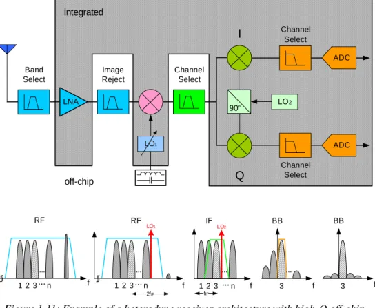
Heterodyne Receiver
Conventional radio transceivers utilize the so called heterodyne architecture (hetero = different, dyne = mix). This architecture, introduced first by [Armst1918], usually has two or more stages for frequency conversion. An example is shown in figure 1.11. A passive bandpass filter limits the input spectrum provided by the anten-na. Due to noise introduced in the mixer, the signal is first amplified in a low noise am-plifier (LNA). Interferers at frequencies symmetrically with fIF to the local oscillator (LO) signal will create images during mixing. Hence, these bands have to be removed by an image reject filter first. For that, the signal goes off-chip into an image rejection (IR) filter using passives with high quality factor. Then, mixing with a tunable LO sig-nal at RF downconverts the selected channel to IF. This LO1 output needs to be varia-ble in small frequency steps for narrow band selection. To alleviate the aforementioned sensitivity-selectivity trade-off in image rejection, an off-chip, high-Q bandpass filter performs partial channel filtering at a relatively high intermediate frequency. A second downconversion mixing step translates the signal down to baseband and further reduc-es the requirements for the final, integrated channel selection filter.
LO2 Band Select LNA 90° I Q integrated off-chip Image Reject Channel Select LO1 Channel Select ADC ADC Channel Select BB f 3 f fIF ... 1 23 ... n IF LO2 f 2fIF RF ... n 1 23... LO1 f RF ... n 1 23... f BB 3 ...
Figure 1.11: Example of a heterodyne receiver architecture with high-Q off-chip filters.Channel selection is done partly at IF and partly at baseband.
Digital modulation schemes, like those presented in section 1.3.1, use both in-phase and quadrature elements of a signal. Both components can be generated in the second mixing stage, as shown in figure 1.11. Since the channel of interest is already selected by the first mixer, the frequency of the second LO is fixed.
Off-chip passive components provide filters with a high Q-factor. This results in good performance for both sensitivity and selectivity and makes the heterodyne archi-tecture a common choice. Furthermore, noise introduced by the local oscillator is less problematic, as it is filtered by subsequent channel selection. The filters can be manu-factured in different technologies, e.g. bipolar and CMOS. However, off-chip filtering comes to the price of extra signal buffering (driving typically 50 Ohm loads), increased complexity, higher power consumption and larger size. Drawbacks that are contradict-ing the goals of increased portability. Examples uscontradict-ing a heterodyne architecture can be found for instance in [Stetz1995], [Fenk1997], [Razav2001], and [Ahola2004].
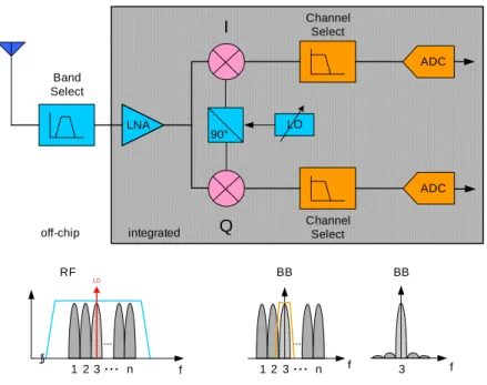
Homodyne Receiver
The homodyne (homo = same, dyne = mix) architecture uses a single frequency translation step to convert the RF channel directly to baseband without operations at intermediate frequencies.
It is therefore also called zero-IF or direct conversion architecture. Figure 1.12 shows this architecture for the case of quadrature downconversion. As in the
hetero-LNA 90° I Q ADC ADC f ... 1 23... n BB f 3 BB integrated off-chip LO Band Select Channel Select Channel Select f ... 1 23... n RF LO
Radio Receiver Architectures 19
dyne case, an off-chip RF filter first performs band limitation, before the received sig-nal is amplified by an integrated LNA. Channel selection is done by tuning the RF frequency of the LO to the centre of the desired channel, making the image equal to the desired channel. Hence, the problem of images is not present, and the off-chip IR filter can be omitted. A subsequent channel selection low-pass filter (LPF) then removes nearby channels or interferers prior to A/D conversion. Channel filtering is now possi-ble entirely on-chip. But since neither image rejection filter nor channel select filtering is done prior mixing, all adjacent channel energy is untreated. This requires the LPF and ADC to have a sharp cutoff profile and high linearity, respectively. In the view of low-Q values of integrated components this implies tougher design challenges.
A severe problem in homodyne receivers are DC offsets. If one mixer input contains signal components from the second input, then mixing will generate a DC component. Caused by leakage from the local oscillator to the LNA (or vice versa), self-mixing will corrupt the baseband signal at DC and saturate subsequent processing blocks. If the re-ceiver moves spatially, it receives reflected LO signals at the antenna which generates time varying offsets. These DC offsets need to be compensated. One technique is to disregard a small part of the signal band close to DC and employ a high-pass filter with very sharp cutoff profile at low corner frequencies. This requires large time constants, and hence, large capacitors, i.e. area. It is only practical for wide-band applications, where the loss of a few tens of hertz bandwidth at DC does not degrade the receiver performance significantly. For narrow band applications, this would cause large per-formance losses. Alternatively, in non-continuous transmission schemes, e.g. TDMA access, the DC offset can be periodically sensed and compensated by the receiver dur-ing the quiescent time intervals. Compensation is either carried out prior to the ADC, or in the digital domain using digital-to-analog conversion in a feedback path.
Due to direct conversion to DC, homodyne receivers are more susceptible to distur-bances arising from I/Q phase mismatches, nonlinearities and flicker noise than hetero-dyne designs. To control the performance loss, additional circuitry and design efforts are required. However, there is no need for image rejection or other off-chip filters, saving power and total receiver volume. Its monolithic integration capabilities make the homodyne architecture an attractive alternative for wireless receivers. More infor-mation regarding cancellation of offset and other limitations, can be found e.g. in [Abidi1995], [Yoshi1998], [Razav1997], [Matin2000], [Namgo2001], [Cheun2001], [Faulk2002], [Sohn2002], and [Cao2004]. If the RF signal is downconverted in a sin-gle step to a low (but not to DC) frequency, then limitations at DC have less impact on the receiver performance. This approach is followed in low-IF architectures.
Low-IF
In a low-IF architecture, example shown in figure 1.13, an off-chip bandpass filter performs band selection prior to amplification by an LNA. In order to overcome the drawbacks associated with the homodyne architecture, the RF signal is downconverted to a frequency close to the baseband, but not including DC (typically between a several 100 kHz and few MHz). Hence, the problem of DC-offset is eliminated, and the effects of flicker noise and distortion are notably reduced. Furthermore, the conversion is done in a single step and all subsequent filtering can be performed on-chip. This improves integration capabilities. Similar to zero-IF, a tuneable local oscillator selects the de-sired RF channel. However, the image from downconversion is now different from the wanted signal and it has to be taken care of after the mixing stage. This can be achieved with integrated complex bandpass filters or in the digital domain using DSPs. Howev-er, gain and phase errors originating from mismatches in the quadrature mixing limit the image suppression. Compared to the homodyne architecture, power consumption is increased (due to analog-to-digital conversion at IF). Moreover, bandpass filter and ADC have to deal with double as wide bandwidth. Further details on low-IF receiver architectures can be found for instance in [Seven1994], [Gray1995], [Crols1995], [Crols1998], [Adise2002], and [Fang2005].
Band Select 90° I ADC ADC LO Q f 3 BB integrated off-chip Channel Select Channel Select LNA f ... 1 23... n BB f ... 1 23... n RF LO
Radio Receiver Architectures 21
Wideband-IF
An alternative to the designs above is the wideband-IF architecture shown in figure 1.14. Signals that passed the off-chip band selecting filter are amplified in the LNA and are then downconverted to IF. In contrast to the previous architectures, the first local oscillator frequency is fixed. All available channels are converted to inter-mediate frequency, resulting in a wide bandwidth at IF. Upconverted frequency com-ponents are removed by a simple low-pass filter. Channel selection and filtering are done at IF. The requirements for the tuneable LO and low-pass filter in the second downconversion stage are relaxed due to the lower operation frequency. Hence, a nar-row channel can be selected and filtered without off-chip components. Furthermore, filtering can be performed partly in the digital domain, which adds to multi-standard operation capabilities of this architecture. This flexibility comes to the expense of higher linearity requirements of the ADC.
Since the first local oscillator output is fixed and different from the channel frequen-cies, the problem of DC offset is alleviated in the wideband-IF architecture. The still existing self-mixing in LO1 or LO2 results in constant DC offsets that can be removed either in analog or digital domain. Isolation from the channel selection oscillator (LO2) to the antenna is much larger than in the heterodyne case. This greatly reduces prob-lems associated with time varying offsets. Using a fixed frequency at LO1 allows for
Band Select LNA 90° I Q integrated off-chip Channel Select LO1 LPF ADC ADC Channel Select LO1 f RF ... n 1 23... LO2 f ... 1 23... n BB f 3 BB f IF ... n 1 23... LO2
phase noise optimization for this oscillator [Rudel1997]. Frequency conversion to IF introduces images again. These can be removed using a Weaver architecture [Weave1956], but mismatches between the I and Q paths limit the image suppression. Also, additional components from the second conversion stage inevitably result in larger power consumption. These problems are balanced by good monolithic integra-tion capabilities and improved multi-standard prospects due to programmable filtering in the DSP. Further information on wideband-IF architectures can be found for in-stance in [Rudel1997] and [Bernd2003].
2. Sigma-Delta Modulation
This chapter reviews the principle of sigma-delta modulation and characterizes different noise shaping topologies, e.g. low and higher order modulators, single and multi-bit quantiza-tion, as well as continuous time modulation. At the end, design challenges are presented.
2.1 The Modulation Principle
Digital signal processing relies on discrete samples of data. According to the Nyquist theorem, [Nyqui1928] and [Shann1949], the sampling (or processing) fre-quency, fs, has to be at least twice as large as the bandwidth of the input signal, fB, to obtain an unambiguous reproduction of the signal. If this theorem is not fulfilled, alias-ing will occur and information is lost. Data converters usalias-ing fs= fNy= 2·fB are hence called Nyquist converters. However, for reasons of noise margin and filter design com-plexity, a sampling speed of fs> fNy is usually applied.
As has been shown in literature, e.g. [Johns1997], the process of quantization can be modelled a process where the output y(n) is determined from the input sample x(n) plus an additive noise component e(n) as shown in figure 2.1. With the assumption that the additive quantization noise is independent and has white distribution, its power Pe is derived to equal ∆2 /12, where ∆ corresponds to the quantization step size. Therefore, the spectral density of the quantization noise, Se(f) is constant for a certain ∆.
+
e(n)
x(n)
y(n)
x(n)
y(n)
=
Sampling at a frequency much higher than the Nyquist rate is called oversampling and the rate by which fs exceeds fNy is called the oversampling ratio, OSR
(2.1)
Due to the white noise assumption, a larger sampling frequency causes the constant quantization noise power to be distributed over a larger spectrum. This reduces the noise power in the band of interest, fB. A filter that limits the band to fB cuts off all noise components for f > fB reducing the remaining quantization noise power, Pe0, within DC and fB. It can be shown [Norsw1997] that the quantization noise power is decrease by a factor OSR. Each doubling of the oversampling ratio decreases the quan-tization noise power by a factor of two.
(2.2)
The technique of sigma-delta (or delta-sigma) modulation originates from the 1960‘s [Inose1963] and 70‘s [Candy1974]. Its name is derived from the difference and summing nodes in a loop configuration. Additional to oversampling, sigma-delta (Σ∆) modulators modify the spectral properties of the quantization noise. They are said to shape the noise spectral density, Se(f), such that it is low in the band of interest and high elsewhere. This spectral shaping results from a negative feedback loop system as shown in figure 2.2. Here, the linear quantizer model from figure 2.1 is employed. Sig-nal input x(n) and quantization noise contribution e(n) are assumed to be independent, leading to an examination using the superposition principle. With the help of the z-transform, the output is described as
OSR fs fNy --- fs 2fB ---= = Pe0 ∆ 2 12 --- 1 OSR ---⋅ =
+
E(z)
X(z)
+
H(z)
Y(z)
-Figure 2.2: Linear model of sigma-delta modulator (1st order) with injection of quantization noise E(z) in the quantizer.
The Modulation Principle 25
(2.3) where H(z) denominates a generic filter function. Two transfer functions can be de-rived: A Signal Transfer Function (STF) and a Noise Transfer Function (NTF):
(2.4)
(2.5)
With equations (2.4) and (2.5), the loop output is determined as:
(2.6) In order to minimize the effect of quantization noise at the output, the NTF(z) should reach its minimum in the band of interest. That is achieved when H(z) reaches its max-imum, i.e. has a pole. However, STF(z) would be close to unity for a maximum of H(z), leaving the input signal almost unchanged.
First order noise shaping can be obtained by choosing the pole of H(z) to be located at DC. A straightforward integrator satisfies this requirement having
(2.7) A possible implementation of a first order sigma-delta modulator is shown in figure 2.3. It is also called a single-loop, first order modulator architecture. With equa-tion (2.7), the signal transfer funcequa-tions becomes a simple delay
Y z( ) = (X z( )–Y z( ))⋅H z( )+E z( ) STF z( ) Y z( ) X z( ) ---≡ H z( ) 1+H z( ) ---= NTF z( ) Y z( ) E z( ) ---≡ 1 1+H z( ) ---= Y z( ) = SFT z( )⋅X z( )+NTF z( )⋅E z( )
+
e(n)
x(n)
+
z
-1y(n)
-
+
Figure 2.3: First order sigma-delta modulator with discrete time integrator.
H z( ) 1
z–1 ---=
(2.8)
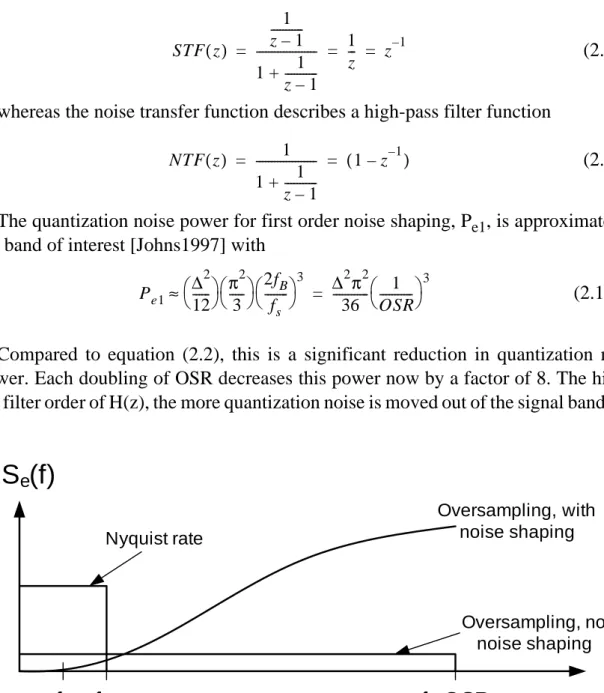
whereas the noise transfer function describes a high-pass filter function
(2.9)
The quantization noise power for first order noise shaping, Pe1, is approximated in the band of interest [Johns1997] with
(2.10)
Compared to equation (2.2), this is a significant reduction in quantization noise power. Each doubling of OSR decreases this power now by a factor of 8. The higher the filter order of H(z), the more quantization noise is moved out of the signal band fB.
It should be noted, however, that sigma-delta modulation only alters the spectral properties of the quantization noise. The noise power is shifted to higher frequencies and still needs to be removed from the signal by means of low-pass filtering. In fact, the total amount of quantization noise increases for higher modulation orders. The
fil-STF z( ) 1 z–1 ---1 1 z–1 ---+ --- 1 z --- z–1 = = = NTF z( ) 1 1 1 z–1 ---+ --- (1–z–1) = = Pe1 ∆ 2 12 --- π2 3 --- 2fB fs --- 3 ≈ ∆2π2 36 --- 1 OSR --- 3 =
f
Bf
Nyf
B·OSR
f
S
e(f)
Nyquist rate Oversampling, no noise shaping Oversampling, with noise shapingFigure 2.4: Noise density of sigma-delta modulation for 1st and 2nd order noise shaping compared to Nyquist rate and oversampling.
Modulator Topologies 27
tering is achieved by means of a decimation filter which also reduces the sampling rate and thereby the number of samples to be processed in DSPs.
2.2 Modulator Topologies
Sigma-delta modulators find a wide range of applications in data conversion sys-tems, especially where high signal-to-noise ratios (SNR) are required. As indicated in equation (2.10), the reduction in noise power comes at the expense of a high sampling speed. This inherently limits the application range of this modulation technique. For instance, employing an oversampling ratio of OSR = 128 for a 20 kHz input signal, quires a sampling speed of 5.12 MHz. This relatively low sampling speed does not re-sult in implementation difficulties. However, if the input is a wideband signal, of say 5 MHz, a sampling rate of fs= 1280 MHz is needed. A high sampling rate naturally has a negative effect on power consumption. Also, some circuit technologies, e.g. CMOS switched capacitor designs, are not suitable for high speed operation in the GHz range. Hence, sigma-delta modulation has long been used in audio and narrow band applications. In recent years however, modulators with input bandwidth extending into the MHz range have been reported, e.g. [Fujim2000], [Geert2000a], [Tabat2000], [Burge2001], [Salo2001], [Vleug2001], [Dezza2003], [Veldh2002], [Veldh2003].
To maintain a reasonable power consumption, the oversampling rate must be re-duced for wideband applications, resulting in insufficient removal of quantization noise. Thus, a different approach than brute force sampling rate increase must be taken. Some options to expand the signal bandwidth while maintaining a high signal-to-quan-tization noise ratio (SNDR) are summarized below.
Higher Order Modulation
In a first order modulator, the quantization error from the previous sample is sub-tracted from the present sample. Higher order modulation is achieved by adding more integration stages. This results in a sharper high-pass filter transfer function H(z) and shapes the quantization noise more aggressively out of the input signal band. In gener-al, a modulator of Mth order exhibits an M times better noise shaping property com-pared to a first order modulator, whereas the input is only delayed by a factor of M. The SQNR improves by about (6·M+3) dB per octave of fs [Johns1997]. Equation (2.11) presents a general modulator transfer function for an Mth order sigma-delta modulator.
(2.11) The single loop topology in figure 2.5(a) is a straightforward extension of the simple first order architecture presented in figure 2.3. Several integration stages are accom-modated in a single loop. The gain stages in the feedback path adjust signal amplitudes. Local feedback (or local resonators), introduced in [Fergu1991], can be added to shift the NTF zeros away from DC to further reduce the inband noise power. A one bit quan-tizer reduces the DAC implementation in the feedback path to a simple switch with good linearity.
An architecture using feed forward of the input signal, figure 2.5(b), has been pro-posed in [Steen1998] and [Silva2001] and was further developed in [Gothe2003]. It ap-proaches the problem of integrator nonidealities such as finite slew rate and gain for wideband applications at low oversampling ratios. The reduced sensitivity to circuit nonidealities derives from decoupling of sensitive circuits from the input signal. The
Y z( ) = X z( )⋅z–M+E z( )⋅(1–z–1)M
-+
-+
-+
DAC in out α β γ δ-+
+
DAC in+
out 2Figure 2.5: Single loop higher order modulators: (a) chain of inverters and
local resonators; (b) low distortion feed forward architecture
(a)
Modulator Topologies 29
integrator stages ideally only process quantization noise, reducing their performance requirements.
Major limitations to high order, single loop structures are concerns of stability. If the input signal level to the quantizer exceeds its normal range, the quantizer becomes overloaded, i.e. the quantization error becomes larger than ±∆/2. The system might not be able to return to a stable state even if the quantizer input returns to low values. The larger the number of integrators, the higher the risk to overload the quantizer. Solutions to this problem lie in adding sensing circuitry to reset the modulator in the event of in-stability or by reducing the input signal level. The latter method impacts the dynamic range performance, and hence, the sensitivity of the total receiver. Different methods for this are discussed for instance in [Johns1997].
Alternative topologies are cascaded (MASH) modulator architectures. They employ 2 or more modulator loops, each comprising a low order modulator to maintain stabil-ity. Each following loop processes only the quantization noise of the previous loop, which improves the total resolution. The quantization noise of the following loops is subtracted from the output of the first loop in a digital error cancellation logic, further reducing the total quantization noise. An architecture with four integration steps ar-ranged in two 2nd order loops is shown in figure 2.6. This 2-2 MASH modulator pro-vides 4th order noise shaping. The DACs in the feedback paths have the same resolution as their corresponding quantizers, e.g. 1 bit.
The MASH topology was first introduced in [Matsu1987] and quickly gained much interest in sigma-delta applications. The main advantage of a MASH architecture is the high degree of noise shaping without emerging stability problems. In theory, there is
-+
-+
DAC in out+
+
-+
DAC Delay Error Cancellation Logicno limit on how many cascades can be used. However, cascaded modulators require very good matching between analog and digital processing paths. In practice, the sec-ond and following loops do not only process noise and the quantization error is not can-celled completely resulting in leakage noise at the modulator output. Furthermore, internal signal level scaling impacts the dynamic range. In order to improve matching, bigger analog components are used, increasing the silicon area. The larger number of components also contributes to a higher power consumption.
Error Feedback Structure
A modulator using a noise shaping filter in the feedback part is the error feedback topology shown in figure 2.7 [Anast1989], [Norsw1997]. Its transfer functions are readily derived as STF = 1 and NTF = G(z)-1. This modulator leads to simple circuit implementations. An important drawback, however, is its susceptibility to analog com-ponent mismatch. The zeros of the NTF, i.e. G(z) = 1, are not created by a large DC gain. Therefore, small coefficient mismatches cause the remaining quantization noise. Hence, this circuit is more suitable for digital modulator implementations, where no component mismatches occur.