1
Growth of epitaxial SiGe alloys as etch-stop layers in germanium-on-insulator fabrication
Ahmad Abedin, Konstantinos Garidis, Ali Asadollahi, Per-Erik Hellström, and Mikael Östling
KTH Royal Institute of Technology, School of Electrical Engineering and Computer Science, SE-164 40 Kista, Sweden
Abstract
In this study, the application of epitaxially grown SixGe1-x films as etch stop layers in a germanium-on-insulator substrate fabrication flow is investigated. Layers with Ge contents from 15% to 70% were epitaxially grown on Si (1 0 0) using silane and germane. It was found that the Ge content in the films is independent of the growth temperature for fixed partial pressure ratios. At low growth temperatures the activation energy is found to be 1.8 eV which points to a hydrogen desorption limited growth rate mechanism. At growth temperatures of less than 500 ℃, the surface roughness is <1 nm. This surface roughness does not change when the films are grown on Ge substrates. Finally, a fully strained Si0.5Ge0.5 film was grown on Ge strain relaxed buffer at 450 ℃. This layer demonstrates etch selectivity of >400:1 towards Ge in diluted SC-1. This result enables the integration of the Si0.5Ge0.5 film as an etch stop layer for single crystalline germanium-on-insulator substrate fabrication.
2
Introduction
New materials and technologies are required to fabricate faster electronic devices and circuits with lower power consumption. 3D integration is a promising technology to reduce interconnect lengths and increase the packing density of devices by stacking transistors on top of each other in tiers, connected with inter tier vias [1,2]. 3D integration give the possibility to integrate different devices such as memories, optical communication components, sensors and energy sources on a single chip to achieve multi functionality. The sequential 3D integration technology enables a high density of inter tier vias between device tiers. However, there are challenges to implement sequential 3D integration, with one of the most important one being the limited thermal budget available during device fabrication [3]. The processing temperature of the top tier devices must be compatible with the fabricated devices in the bottom tier devices and interconnects, typically limiting the process temperature to less than 550 °C [3,4]. Ge with its inherently lower processing temperature is a candidate device material in sequential 3D integration. Ge based sequential 3D integration requires formation of single crystalline Ge on an amorphous inter-layer dielectric (GOI) at a low temperature which excludes fabrication schemes requiring high temperature processing such as condensation [5–7] or lateral overgrowth [8]. However, low temperature direct wafer bonding and etch-back is a promising method for fabrication of the top tier devices in monolithic 3D integration [9]. In such processes, a good etch-stop layer is required in order to remove the sacrificial wafer while keeping the thin active layer intact. Etch stop SixGe1-x layers have been routinely used for silicon-on-insulator fabrication [REF]. Its application can be extended to GOI fabrication as well. This layer should have a good etch selectivity toward Ge. SixGe1-x is a good candidate for this purpose since it can have high etch selectivity toward Ge, does not add any residual dopants to the layer, can be grown fully strained on Ge and does not induce any crystal defects. . From a sequential 3D integration point of view, this can have the added benefit of a one step process: epitaxial growth of the complete layer stack can be done in a single epitaxial step without breaking vacuum. It is of particular importance for the next generation Ge technology, to enable a reproducible and robust technique for GOI fabrication.
In this work, we have investigated the epitaxial growth of SixGe1-x layers using reduced pressure chemical vapor deposition (RPCVD), as an etch-stop layer in the fabrication of single crystalline GOI substrate and layer transfer. A Si50Ge50 layer has been successfully implemented as an etch stop layer in a GOI fabrication process as shown in [10].
Experimental details
In this work, 100 mm Si (001) substrates have been used. All samples were subjected to standard clean (NH4OH:H2O2:H2O [1:1:5] + HCl:H2O2:H2O [1:1:5]) and 5% HF dip before loading into the load-lock of the epitaxy tool. Epsilon 2000 RPCVD tool from ASM has been used for the epitaxial growth of the layers. The films were grown at temperatures ranging from 450 °C to 650 °C by using silane (SiH4) and germane (10% GeH4 in H2) as sources for Si and Ge. The flow rate of SiH4 was kept constant at 90 sccm for all the samples, and the flow rate of 10 % GeH4 in H2 was varied from 50 to 500 sccm. The reactor pressure was kept at 2666 Pa and 20 slm of H2 was used as the
3
carrier gas. The layers were first grown on Si wafers to evaluate the growth conditions and achieve fully-strained Si1-xGex with high crystal quality and smooth surface. Then the Si1-xGx layers were grown on Ge strain-relaxed buffers (SRB) for GOI fabrication. In the GOI fabrication the Si1-xGx layer serves as an etch stop layer towards Ge. The targeted Ge concentration x=0.5 was selected since Si0.5Ge0.5 layers have been shown to be possible to grow up to 20 nm thickness on Si without plastic deformation at a low temperature of 500 °C [11]. Fully strained Si0.5Ge0.5 layers with low defect concentration on top of Ge SRB can function as effective etch-stop layers in the GOI fabrication process.
The thickness and the Ge content of the films were measured by Spectroscopic Ellipsometry (SE), high resolution X-Ray diffraction (HRXRD), and weighting. SE measurements were performed in the photon energy range of 1.5-4.5 eV, the light spot size of 100 µm x 300 µm, immediately after the sample growth using Horiba UVISEL ER tool. The SE wafer mapping (25 points of measurements with 10 mm edge of exclusion) was performed on the Si1-xGex thin films grown at various temperatures to evaluate the thickness homogeneity over the wafer. A Philips X’Pert Panalytical tool with a copper x-ray source, a 4 bounce symmetric Ge (220) monochromator was used for XRD measurements. Differential weighting characterizations were also used to confirm the thickness and Ge concentration measurements.
SiGe growth using SiH4 and GeH4
The concentration of Ge (x) in Si1-xGex layers as a function of the partial pressure ratio of GeH4 (PGeH4) to SiH4 (PSiH4) is shown in Figure 1(a). The partial pressure of SiH4 was held constant to 12 Pa and the incorporated Ge concentration in the Si1-xGex layers is found to increase with increasing GeH4 partial pressure in accordance with literature [12–15]. Assuming that the concentration of Ge in the growing Si1-xGex film is govern by the impingement rate of SiH4 and GeH4 times their respective sticking coefficients SiH4 and GeH4, the inverse of the Ge concentration can be expressed as:
4 1 𝑥= 1 + √ 𝑚𝐺𝑒𝐻4 𝑚𝑆𝑖𝐻4 𝜎𝑆𝑖𝐻4 𝜎𝐺𝑒𝐻4 𝑃𝑆𝑖𝐻4 𝑃𝐺𝑒𝐻4 (1)
where mGeH4 and mSiH4 is the mass of GeH4 and SiH4, respectively. In Figure 1(b) the inverse of x
versus the ratio of PSiH4 to PGeH4 is plotted. The solid line displays Eq. (1) fitted to the data with the ratio of the sticking coefficients as fitting parameter. From the slope of the line we extract that the sticking coefficient of SiH4 is 0.15 times the sticking coefficient of GeH4. Figure 2 shows the Ge concentration x at a fixed partial pressure of GeH4 to SiH4 versus growth temperature. The Ge concentration in the growing Si1-xGex film is independent of the growth temperature, indicating that the ratio of the sticking coefficients is temperature independent within the investigated temperature range of 450 °C to 560 °C.
(a) (b)
Figure 1. (a) Ge content in the Si1-xGex layer plotted over increased partial pressure ratios of GeH4 to SiH4 for growth at 450 °C and 560 °C. SiH4 partial pressure was held constant to 12 Pa. The data are plotted in (b) with the ratio of SiH4 to GeH4 sticking coefficients as the fitting parameter according to Eq. 1.
5
Figure 2. The Ge content in the Si1-xGex film is independent of the growth temperature for fixed partial pressures of GeH4 and SiH4.
An Arrhenius plot of the Si0.45Ge0.55 growth rate is shown in Figure 3. At growth temperatures below 560°C the growth rate displays an Arrhenius dependence with an activation energy of 1.8 eV. At low temperature the growth rate of Si from SiH4 is known to be limited by hydrogen desorption with an activation energy of 2.1 eV [16]. Germanium is known to increase the growth rate compared to Si and to have a catalytic effect on the hydrogen desorption. The activation energy for hydrogen desorption on Ge from GeH4 has been experimentally determined to be 1.65 eV [17]. The activation energy of 1.8 eV is between those found for Si and Ge. This activation energy is consistent with the observation that the growth rate of Si0.45Ge0.55 from SiH4 and GeH4 is limited by hydrogen desorption at low temperature. Although the growth rate decreases with decreasing temperature, and is only 2.5 nm/min at 450 °C, it is still practical to grow fully strained Si0.45Ge0.55 layers with thicknesses below 40 nm. At temperatures above 560°C, the growth rate deviates from an Arrhenius behavior and saturates at 70 nm/min due to limited supply of SiH4 and GeH4.
Figure 3: Arrhenius plot of the growth rate of Si0.45Ge0.55 grown with SiH4 and GeH4 pressures fixed at 12 Pa and 2.9 Pa respectively.
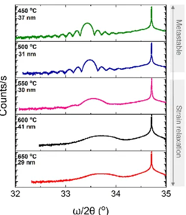
Conventional ω-2θ HRXRD scan around the (004) Bragg peak was performed on 40 nm Si0.45 Ge0.55 layers grown at different temperatures ranging from 450°C to 650°C. The peak at 34.7 ̊ is related to the Si substrate and the peak at 33.4 ̊ is related to Si0.45Ge0.55 layer. The well-defined thickness fringes beside the Si0.45Ge0.55 peak of the layer grown at 450 and 500℃ shows that the layer is fully strained with flat interfaces. This indicates that defects are not formed at the interface of Si0.45Ge0.55/Si. The location of the peak at 33.4° and the concentration x=0.55 determined from spectroscopic ellipsometry infers that the Si0.45Ge0.55 is 1.3% compressively strained. As the temperature increases from 450 °C to 650 °C, the angular separation of the Si0.45Ge0.55 peak from the Si substrate peak decreases. Increasing the growth temperature induces strain relaxation and the Si0.45Ge0.55 films grown at temperatures higher than 500 °C were partially strain relaxed.
6
Because of strain relaxation, defects are formed at the interface of Si0.45Ge0.55/Si which results in peak broadening and lack of thickness fringes in the ω-2θ HRXRD scans.
Figure 4. ω-2θ scan around the (004) x-ray diffraction Bragg peak of the Si0.45Ge0.55 layers grown at T=450 – 650 °C.
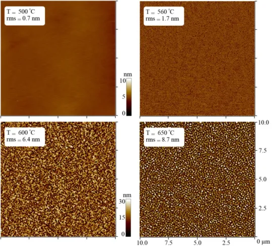
The surface morphology of Si0.45Ge0.55 layers grown on Si at different temperature from 500 °C to 650 °C measured with atomic force microscope (AFM) are shown in figure 5. The AFM images show that when growth temperature is lower than 500 °C the surface roughness is kept below 1 nm. Layers grown at temperatures higher than 500 °C exhibited an increased surface roughness which correlates with the growth temperatures where strain relaxation occurs, which has also been reported by Hartman et. al.in [11].
7
Figure 5. 10 µ𝑚 × 10 µ𝑚 atomic force microscopy (AFM) images of the Si0.45Ge0.55 surfaces grown at P(GeH4)/P(SiH4) = 0.24 in a temperature range of (a) 500 oC, (b) 560 oC, (c) 600 oC, and (d) 650 oC. Surface root-mean-square (rms) roughness and the growth temperatures are provided in each image.
Si0.5Ge0.5 on Geas an etch stop layer for GOI fabrication
The GOI fabrication process is explained in detail our previous work in [10]. In short, this process employs a single epitaxial growth step, room temperature wafer bonding and a etch-back process. For a Si1-xGex layer to be integrated in such a process flow the Ge concentration needs to be controlled to about 50 % and thicknesses less than 30 nm has to be grown with good uniformity. Furthermore, the surface roughness <1nm is required for successful bonding. An additional property the Si1-xGex layer is to have a high etch selectivity towards Ge. Following the layer development reported in the previous section, a Si0.5Ge0.5 layer was grown on Ge strain relaxed buffer (SRB) and etched in diluted SC-1 (NH4OH:H2O2:H2O, 1:1:500) in order to evaluate the etch selectivity to Ge.
The HRXRD rocking curve of 20 nm Si0.5Ge0.5 grown on Ge SRB is shown in Fig. 6. The peak at 34.7 ̊ is related to the Si substrate and the peak at 33.2˚ is related to Ge SRB. The peak associated to Si0.5Ge0.5 layer can be seen at 34.5° with small fringes in the left side. The low intensity of the fringes compared to the layers grown directly on Si is due to lower thickness of the Si0.5Ge0.5 layer
8
and slightly higher surface roughness of Ge SRB (RMS<1nm) compared to Si substrate. The position of the peak has also moved from 33.4° on Si to 34.5° on Ge, indicating that the Si0.5Ge0.5 layer is 1.6 % tensile strained when grown on relaxed Ge. .
Figure 6. Conventional ω-2θ scan around the (004) x-ray diffraction Bragg peak of the Si0.5Ge0.5 layer grown on Ge strain relaxed buffer.
The surface morphology of Ge buffer and Ge buffer capped with 10 nm Si0.5Ge0.5 is shown in Figure 7. The AFM images show that the surface roughness of the layer stack is not increased when Si0.5Ge0.5 layer is deposited on top of Ge SRB at temperatures as low as 450°C. Low surface roughness makes it a suitable material for wafer-bonding and layer transfer application.
Figure 7. AFM image of Si0.5Ge0.5 layer grown on Ge strain relaxed buffer. The RMS surface roughness does not change with the deposition of Si0.5Ge0.5 on top of the Ge SRB.
9
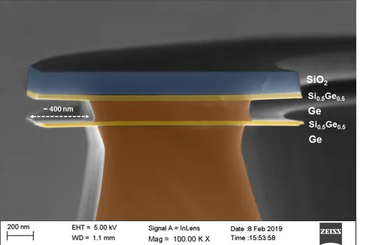
In order to test the efficiency of the Si0.5Ge0.5 etch stop layer, the stack in Figure 8 was grown on a 2 μm Ge strain relaxed buffer. Structures of various sizes were patterned with i-line lithography on the layer stack. The photoresist was subsequently removed in O2 plasma. Reactive ion etching (HBr, Cl2 and He-O2) with PECVD SiO2 as a hard mask was applied to etch the Ge/SiGe/Ge/SiGe layer stack.
Figure 8. Schematic of the stack grown to test the efficiency of the Si0.5Ge0.5 etch stop layer in diluted SC-1.
Diluted SC-1 was dispensed for 80 s on the wafer using an automatic etch spray tool. Figure 9 shows a cross section SEM image of the wafer after the wet etch process. It is clear that the Si0.5Ge0.5 remains intact after 80 s of etch while the Ge is recessed by approximately 400 nm. The etching shows a selectivity of >400:1 towards Si0.5Ge0.5. The etch stop behavior is based on the formation of a thin SiO2 film around the Si0.5Ge0.5 which essentially stops further etching. This mechanism is described in detail in reference [10] where a 10 nm thin Si0.5Ge0.5 is grown with SiH4 and GeH4 on 25 nm of high quality crystalline Ge. This film is then successfully applied as an etch stop layer during Ge etch in diluted SC-1 for the fabrication of a germanium-on-insulator substrate. This application expands the established use of silicon germanium alloys as etch stop layers from the SOI to GOI fabrication areas. It further demonstrates its success as a key fabrication step in sequential 3D integration.
10
Figure 9. Cross section of the stack shown in Fig. 9 after 80 s of diluted SC-1. The Ge layers are recessed by approximately 400 nm while the Si0.5Ge0.5 layers remain intact.
Conclusions
In this paper, silane and germane were used to grow epitaxial SiGe layers with Ge contents ranging from 15% to 70% was investigated. The growth rate, crystal quality, strain level, and surface morphology of the layers were investigated in order to develop a fully strained SiGe layer with 50% Ge content. This layer was successfully integrated in a stack of Ge/SiGe/Ge/Si, showing minimized surface roughness and thickness inhomogeneity. An etch selectivity of >400:1 towards Si0.5Ge0.5 was achieved when etching Ge in diluted SC-1. This result facilitates the use of the Si0.5Ge0.5 film as an etch stop layer for GOI fabrication, in a similar way to SOI fabrication by using direct wafer bonding and etch back.
References
[1] P. Batude, M. Vinet, A. Pouydebasque, C. Le Royer, B. Previtali, C. Tabone, L. Clavelier, S. Michaud, A. Valentian, O. Thomas, O. Rozeau, P. Coudrain, C. Leyris, K. Romanjek, X. Garros, L. Sanchez, L. Baud, A. Roman, V. Carron, H. Grampeix, E. Augendre, A. Toffoli, F. Allain, P. Grosgeorges, V. Mazzochi, L. Tosti, F. Andrieu, J.-M. Hartmann, D. Lafond, S. Deleonibus, O. Faynot, GeOI and SOI 3D monolithic cell integrations for high density applications, VLSI Technol. Symp. (2009) 166–167.
[2] M. Vinet, P. Batude, C. Fenouillet-Beranger, L. Brunet, V. Mazzochi, C.M.V. Lu, F. Deprat, J. Micout, B. Previtali, P. Besombes, N. Rambal, F. Andrieu, O. Billoint, M. Brocard, S. Thuries, G. Berhault, C.L. Dos Santos, G. Cibrario, F. Clermidy, D. Gitlin, O. Faynot,
11
Opportunities brought by sequential 3D CoolCubeTM integration, in: Eur. Solid-State Device Res. Conf., IEEE, 2016: pp. 226–229. doi:10.1109/ESSDERC.2016.7599627.
[3] P. Shukla, A.K. Coskun, V.F. Pavlidis, E. Salman, An Overview of Thermal Challenges and Opportunities for Monolithic 3D ICs, in: Proc. 2019 Gt. Lakes Symp. VLSI - GLSVLSI ’19, ACM Press, New York, New York, USA, 2019: pp. 439–444. doi:10.1145/3299874.3319485.
[4] A. Vandooren, L. Witters, J. Franco, A. Mallik, B. Parvais, Z. Wu, A. Walke, V. Deshpande, E. Rosseel, A. Hikavyy, W. Li, L. Peng, N. Rassoul, G. Jamieson, F. Inoue, G. Verbinnen, K. Devriendt, L. Teugels, N. Heylen, E. Vecchio, T. Zheng, N. Waldron, V. De Heyn, D. Mocuta, N. Collaert, Sequential 3D: Key integration challenges and opportunities for advanced semiconductor scaling, in: ICICDT 2018 - Int. Conf. IC Des. Technol. Proc., Institute of Electrical and Electronics Engineers Inc., 2018: pp. 145–148. doi:10.1109/ICICDT.2018.8399777.
[5] S. Nakaharai, T. Tezuka, N. Hirashita, E. Toyoda, Y. Moriyama, N. Sugiyama, S. Takagi, Generation of Crystal Defects in Ge-on-Insulator (GOI) Layers in Ge-condensation Process, in: 2006 Int. SiGe Technol. Device Meet., IEEE, 2006: pp. 1–2. doi:10.1109/ISTDM.2006.246534.
[6] J. Suh, R. Nakane, N. Taoka, M. Takenaka, S. Takagi, Effects of additional oxidation after Ge condensation on electrical properties of germanium-on-insulator p-channel MOSFETs, Solid. State. Electron. 117 (2016) 77–87. doi:10.1016/j.sse.2015.11.014.
[7] S. Dissanayake, Y. Shuto, S. Sugahara, M. Takenaka, S. Takagi, (110) Ultrathin GOI layers fabricated by Ge condensation method, Thin Solid Films. 517 (2008) 178–180. doi:10.1016/j.tsf.2008.08.102.
[8] J.H. Nam, T. Fuse, Y. Nishi, K.C. Saraswat, Germanium on insulator (GOI) structure using hetero-epitaxial lateral overgrowth on silicon, in: ECS Trans., 2012: pp. 203–208. doi:10.1149/1.3700469.
[9] G. Taraschi, A.J. Pitera, E.A. Fitzgerald, Strained Si, SiGe, and Ge on-insulator: review of wafer bonding fabrication techniques, Solid. State. Electron. 48 (2004) 1297–1305. doi:10.1016/J.SSE.2004.01.012.
12
[10] A. Abedin, L. Zurauskaite, A. Asadollahi, K. Garidis, G. Jayakumar, B.G. Malm, P. Hellstrom, M. Ostling, Germanium on Insulator fabrication for Monolithic 3D integration, IEEE J. Electron Devices Soc. (2018). doi:10.1109/JEDS.2018.2801335.
[11] J.M. Hartmann, A. Abbadie, S. Favier, Critical thickness for plastic relaxation of SiGe on Si(001) revisited, J. Appl. Phys. 110 (2011). doi:10.1063/1.3656989.
[12] M. Hierlemann, C. Werner, Modeling of SiGe deposition using quantum chemistry techniques for detailed kinetic analysis, Mater. Sci. Semicond. Process. 3 (2000) 31–39. doi:10.1016/S1369-8001(00)00007-X.
[13] J.M. Hartmann, F. Bertin, G. Rolland, M.N. Séméria, G. Brémond, Effects of the temperature and of the amount of Ge on the morphology of Ge islands grown by reduced pressure-chemical vapor deposition, Thin Solid Films. 479 (2005) 113–120. doi:10.1016/j.tsf.2004.11.204.
[14] C.L. Cheng, D.S. Tsai, J.C. Jiang, Study of pathway of hydrogen migration and desorption on SiGe(100) surface using Ab Initio calculations, Japanese J. Appl. Physics, Part 1 Regul. Pap. Short Notes Rev. Pap. 44 (2005) 7625–7633. doi:10.1143/JJAP.44.7625.
[15] M. Imai, Y. Miyamura, D. Murata, T. Kanda, Analytical Model for Epitaxial Growth of SiGe from SiH 4 and GeH 4 in Reduced-Pressure Chemical Vapor Deposition, Jpn. J. Appl. Phys. 47 (2008) 8733–8738. doi:10.1143/JJAP.47.8733.
[16] M. Suemitsu, K. Kim, N. Miyamoto, Role of Ge in SiGe epitaxial growth using silane/germane gas‐source molecular beam epitaxy, J. Vac. Sci. Technol. A Vacuum, Surfaces, Film. 12 (1994) 2271–2275. doi:10.1116/1.579128.
[17] T.J. King, K.C. Saraswat, Deposition and Properties of Low-Pressure Chemical-Vapor Deposited Polycrystalline Silicon-Germanium Films, J. Electrochem. Soc. 141 (1994) 2235–2241. doi:10.1149/1.2055095.