Linköping Studies in Science and Technology
Dissertation No. 1572
Synthesis of Carbon-based and Metal-Oxide Thin Films using High
Power Impulse Magnetron Sputtering
Asim Aijaz
Plasma & Coatings Physics Division Department of Physics, Chemistry and Biology (IFM)
Linköping University SE-581 83 Linköping, Sweden
© Asim Aijaz 2014 ISBN: 978-91-7519-408-0
ISSN 0345-7524 Printed by LiU-tryck Linköping, Sweden, 2014
I
Abstract
The work presented in this thesis deals with synthesis of carbon-based as well as metal-oxide thin films using highly ionized plasmas. The principal deposition method employed was high power impulse magnetron sputtering (HiPIMS). The investigations on plasma chemistry, plasma energetics, plasma-film interactions and its correlation to film growth and resulting film properties were made. The thesis is divided into two parts: (i) HiPIMS-based deposition of carbon-HiPIMS-based thin films and (ii) HiPIMS-HiPIMS-based deposition of metal-oxide thin films.In the first part of the thesis, HiPIMS based strategies are presented that were developed to address the fundamental issues of low degree of carbon ionization and low deposition rates of carbon film growth in magnetron sputtering. In the first study, a new strategy was introduced for increasing the degree of ionization of sputtered carbon via increasing the electron temperature in the discharge by using a higher ionization potential buffer gas (Ne) in place of commonly used Ar. A direct consequence of enhanced electron temperatures was observed in the form of measured large fluxes of ionized carbon at the substrate position. Consequently, high mass densities of the resulting amorphous carbon (a-C) thin films reaching 2.8 g/cm3 were obtained.
In another study, feasibility of HiPIMS-based high density discharges for high-rate synthesis of dense and hard a-C thin films was explored. A strategy was compiled and implemented that entailed coupling a hydrocarbon precursor gas (C2H2) with high density
discharges generated by the superposition of HiPIMS and direct current magnetron sputtering (DCMS). Appropriate control of discharge density (by tuning HiPIMS/DCMS power ratio), gas phase composition and energy of the ionized depositing species lead to a route capable of providing ten-fold increase in the deposition rate of a-C film growth compared to that obtained using HiPIMS Ar discharge in the first study. The increased deposition rate was achieved without significant incorporation of H (<10 %) and with relatively high hardness (>25 GPa) and mass density (~2.32 g/cm3). The knowledge gained in this work was utilized in a subsequent work where the feasibility of adding high
ionization potential buffer gas (Ne) to increase the electron temperature in an Ar/C2H2
HiPIMS discharge was explored. It was found that the increased electron temperature lead to enhanced dissociation of hydrocarbon precursor and an increased H incorporation into the growing film. The resulting a-C thin films exhibited high hardness (~ 25 GPa), mass densities in the order of 2.2 g/cm3 and H content as low as about 11%. The striking feature of the resulting films was low stress levels where the films exhibited compressive stresses in the order of 100 MPa.
In the second part of the thesis, investigations on reactive HiPIMS discharge characteristics were made for technologically relevant metal-oxide systems. In the first study, the discharge characteristics of Ti-O and Al-O were investigated by studying the discharge current characteristics and measuring the ion flux composition. Both, Ti-O and Al-O discharges were dominated by large fluxes of ionized metallic as well as sputtering and reactive gases species. The generation of large ionized fluxes influenced the discharge characteristics consequently surpassing the changes in the secondary electron emission yields which, in the case of DCMS discharges entail contrasting behavior of the discharge voltage for the two material systems. The study also suggested that the source of oxygen ions in the case of reactive HiPIMS is both, the target surface (via sputtering) as well as gas phase.
In a subsequent study, the knowledge gained from the studies on metal-oxide HiPIMS discharges was utilized for investigating the behavior of reactive HiPIMS discharges related to ternary compound thin film growth. In this work Al-Si-O system, which is a promising candidate for anti-reflective and solar thermal applications, was employed to carry out the investigations under varied target compositions (Al, Al0.5Si0.5, and
Al0.1Si0.9). It was found that the discharge current behavior of metal and oxide modes of
Al-Si-O HiPIMS discharges were similar to those of Al-O and were independent of the target composition. The influence of energy and composition of the ionized depositing fluxes on the film growth was also investigated. It was shown that stoichiometric Al-Si-O thin films exhibiting a refractive index below 1.6 (which is desired for anti-reflective applications) can be grown. Furthermore, the refractive index and chemical composition
III of the resulting films were found to be unchanged with respect to the energy of the depositing species.
The effect of ionized deposition fluxes that are generated in metal-oxide HiPIMS discharges was also investigated for the phase composition and optical properties of TiO2
thin films. It was found that energetic and ionized sputtered flux in reactive HiPIMS can be used to tailor the phase formation of the TiO2 films with high peak powers facilitating
the rutile phase while the anatase phase can be obtained using low peak powers. It was also demonstrated that using HiPIMS, these phases can be obtained at room temperature without external substrate heating or post-deposition annealing. The results on plasma and film properties were also compared with DCMS.
V
Populärvetenskaplig sammanfattning
I denna avhandling presenteras resultatet efter studier av tunnfilmssyntes av kol och av metalloxider nyttjande en avancerad plasmametod. Denna metod, som heter högeffektpulsad-magnetronsputtering (på engelska high power impulse magnetron sputtering förkortat HiPIMS), nyttjar det faktum att den tillförda momentaneffekten till plasma kan ökas mångdubbelt genom att pulsa effekten. På så sätt hålles medeleffekten tillräckligt låg så att uppvärmningen inte processutrustningen blir för stor. Genom den höga effekten i plasmat joniseras både sputtergas och beläggningsmaterial mycket effektivt. I arbetet har relationer mellan plasmaegenskaper och de tillverkade skikten undersökts.
I den första delen av avhandlingen, som berör kolfilmer, har en metod utvecklats som ger betydligt högre jonisationsgrad av kolet än vad som hittills har presenterats. Kol är särskilt svårt att jonisera i ett sputterplasma pga liten storlek och hög jonisationsenergi. Den ökande joniseringen har åstadkommits genom att höja plasmaelektronernas energi. Den ökade elektronenergin är ett resultat i att en alternativ sputtergas har använts. Normalt nyttjas argon men här har i stället neon använts. Detta resulterade i att höga beläggningsflöden av enkeljoniserat kol kunde uppmätas. Detta är viktigt vid framställning kolfilmer med hög densitet och hög andel diamantbindningar och resulterande filmer fick en amorf struktur och erhöll en densitet 2.8 g/cm2.
För att öka beläggningshastigheten med kol testades även ett alternativ där inte bara kol som sputtras används utan dessutom den kolinnehållande gasen etyn (även kallad acetylen, C2H2) tillsattes. Detta resulterade i att beläggningshastigheten kunde ökas
tiofalt, men den erhållna filmdensiteten blev något lägre (2.32 g/cm2). Anmärkningsvärt är att vätehalten i filmerna understiger 10 % trots riklig tillgång till väte i processen genom tillförseln från C2H2. Genom att utnyttja datorberäkningar (Monte-Carlo) och data
från litteraturen föreslås den höga beläggningshastigheten och den låga vätehalten bero på: (i) sönderdelning av det tillförda kolvätet genom växelverkan med energetiska
elektroner i plasmat vilket ger fritt kol som kan bidra till filmtillväxten (ii) filmens struktur och väteinnehåll påverkas av bombardemang av energetiska joner från plasmat. Dessa resultat uppmuntrade till ytterligare studier. Denna gång genom att kombinera resultaten presenterade ovan genom att tillsätta både neon och etyn till sputtergasen. Detta resulterade även i detta fall till en ökande elektronenergi, men även till något ökat väteinnehåll i filmerna. I detta fall fick de amorfa kolfilmerna en hårdhet så hög som ~ 25 GPa, en densitet på 2.2 g/cm3 och en vätehalt på 11 %. Utmärkande för dessa filmer vara att de erhöll anmärkningsvärt låga inbyggda spänning, uppmätt till i storleksordningen 100 MPa.
I andra delen av avhandlingen berör studiet av användandet av reaktiv tunnfilmsframställning av olika tekniskt relevanta metalloxider med HiPIMS. Första arbetet inkluderade studiet av Ti-O och Al-O, där plasmaegenskaperna studerades. Det inkluderar urladdningsförloppets beteende och jonflödets sammansättning från plasmat. Vanligtvis styrs plasmat urladdningsförlopp mest av kemin på sputterkällans yta. Undersökningen här visar att vid användandet av HiPIMS är det mer komplicerat än så och stora flöden av syrejoner dominera beteendet.
En uppföljande studie av ett ytterligare mer komplicerat material involverar Al-Si-O av olika sammansättningar. Detta material är en lovande kandidat som en komponent i anti-reflexbehandling av, t.ex. solfångare. Det visade sig att urladdningsföloppet liknade det som uppmättes för Al-O oberoende av Al-Si-sammansättningen som användes (Al0.5Si0.5,
till Al0.1Si0.9). I reaktiva sputterförhållanden där Si-O dominerar förväntas att
elektronproduktionen vid sputterkällan skall dominera urladdningsprocessen, men även i detta fall visade det sig att syrejonerna är den dominerande laddningsbäraren. De filmer som växtes med detta material uppvisar ett lågt brytningsindex, mindre än 1,6 vilket också är önskvärt för tillämpningar i fråga.
Ett annat material som studerats är TiO2, ett material som används som en optisk
ytbeläggning för att erhålla olika optiska fenomen men också för att materialet är fotokatalytiskt vilket kan hålla en yta ren om den utsätts för solljus. Beroende på vilka egenskaper man vill optimera så vill man kunna använda olika faser av TiO2. När man
VII växer material med HiPIMS så kan man nyttja de skapade jonerna för att bombardera skiktet under tillväxt. Med hjälp av detta jonbombardemang kan önskad fas erhållas.
IX
Preface
This Dissertation Thesis comprises of the research work that I carried out during my PhD studies in the Plasma and Coatings Physics Division of the Department of Physics, Chemistry and Biology (IFM) at Linköping University from April 2009 to March 2014. The research was financially supported by the Swedish Research Council (VR).
The results from the research work are presented in the appended papers. Preceding the appended papers, the thesis contains an introduction to the field, the adopted methodology and techniques used for carrying out the research work. The contents of the introductory part are largely based on my Licentiate Thesis No. 1537, HiPIMS-based Novel Deposition Processes for Thin Films, published in June 2012.
Asim Aijaz Linköping, February 2014
XI
Appended Papers
Part I: HiPIMS-based Deposition of Carbon-based Thin Films1. A strategy for increased carbon ionization in magnetron sputtering
discharges
Asim Aijaz, Kostas Sarakinos, Daniel Lundin, Nils Brenning, Ulf Helmersson Diamond and Related Materials, 23 (2012) 1.
2. Principles for designing sputtering-based strategies for high-rate
synthesis of dense and hard amorphous carbon thin films
Asim Aijaz, Kostas Sarakinos, Mohsin Raza Khan, Jens Jensen, Ulf Helmersson
Accepted for publication in Diamond and Related Materials, February 2014.
3. Synthesis of amorphous carbon thin films using acetylene-based high
power impulse magnetron sputtering discharges
Asim Aijaz, Sascha Louring, Jens Jensen, Kostas Sarakinos, Ulf Helmersson In final preparation.
Part II: HiPIMS-based Deposition of Metal-Oxide Thin Films
4. Understanding the discharge current behavior in reactive high power
impulse magnetron sputtering of oxides
Montri Aiempanakit, Asim Aijaz, Daniel Lundin, Ulf Helmersson, Tomas Kubart
Journal of Applied Physics, 113 (2013) 133302.
5. Exploring the potential of high power impulse magnetron sputtering for
the synthesis of Al-Si-O based scratch-resistant, antireflective coatings Asim Aijaz, Montri Aiempanakit, Stefan Bruns, Ulf Helmersson, Michael Vergöhl and Kostas Sarakinos
In preparation.
6. Effect of peak power in reactive high power impulse magnetron
sputtering of titanium dioxide
Montri Aiempanakit, Ulf Helmersson, Asim Aijaz, Petter Larsson, Roger Magnusson, Jens Jensen and Tomáš Kubart
Contribution to the appended papers
In Paper I, I was involved in planning of the study, performed all experiments, took part in the analysis of the results and wrote a major part of the paper.In Paper II, I was responsible for planning of the study, performed a large part of film characterization, performed simulations, performed analysis of the results and wrote the paper.
In Paper III, I lead the planning of the study, performed film synthesis and major part of film characterization, performed plasma characterization, analyzed the results and wrote the paper.
In Paper IV, I was involved in planning of the study, took part in all experiments and analysis of the results and co-wrote the paper.
In Paper V, I was involved in planning of the study, performed film synthesis and plasma characterization, took part in the analysis of the results and wrote the paper. In Paper VI, I was involved in planning of the study, took part in film synthesis and characterization, performed plasma characterization and took part in writing the paper.
XIII
Other Publications
1. Patent: Sputtering process for sputtering a target of carbon
Ulf Helmersson, Nils Brenning, Asim Aijaz SE 536285 (C2), WO 2012/138279 (A1).
2. Dual-magnetron open field sputtering system for sideways deposition of thin films
Asim Aijaz, Daniel Lundin, Petter Larsson, Ulf Helmersson Surface and Coatings Technology, 204 (2010), 2165-2169.
3. A novel high-power pulse PECVD method
Henrik Pedersen, Petter Larsson, Asim Aijaz, Jens Jensen and Daniel Lundin Surface and Coating Technology, 206 (2012), 4562-4566.
4. Deposition of yttria-stabilized zirconia thin films by high power impulse magnetron sputtering and pulsed magnetron sputtering
Steffen Sønderby, Asim Aijaz, Ulf Helmersson, Kostas Sarakinos, Per Eklund Accepted for publication in Surface and Coatings Technology (December 2013).
Conference contributions
1. Highly ionized carbon plasmas for the growth of diamond-like carbon thin films using magnetron sputtering, International Conference on Metallurgical Coatings and Thin Films (ICMCTF), April 2013, San Diago, U.S.A.
Contributing author to an oral presentation
2. Synthesis of wear resistant, anti-reflective Al-Si-O thin films using reactive high power impulse magnetron sputtering: Investigations on the plasma composition and plasma energetics, Reactive Sputter Deposition (RSD), December 2012, Ghent, Belgium.
Oral presentation
3. Highly ionized carbon fluxes for the growth of diamond-like carbon films using magnetron sputtering, International Conference on Diamond and Carbon Materials (ICDCM), September 2012, Granada, Spain.
Oral presentation
4. Highly ionized carbon fluxes for the growth of diamond-like carbon films using magnetron sputtering, European Material Research Society (E-MRS), May 2012, Strasbourg, France.
Oral presentation
5. Towards achieving a high degree of carbon ionization in magnetron sputtering discharges, Reactive Sputter Deposition (RSD), December 2011, Linköping, Sweden.
Oral presentation
6. Towards achieving a high degree of carbon ionization in magnetron sputtering discharges, American Vacuum Society (AVS), October 2011, Nashville, U.S.A.
Oral presentation
7. Towards synthesizing high density and sp3 rich carbon films using high power impulse magnetron sputtering, International Conference on HiPIMS, June 2011, Braunschweig, Germany.
Oral presentation
8. Dual-magnetron open field sputtering system for sideways deposition of thin films 12th International Conference on Plasma Surface Engineering (PSE), September 2010, Garmisch-Partenkirchen, Germany.
XV
Acknowledgements
Through the course of this journey which extended over six years at Linköping University, there are many people who have contributed substantially towards my success. I would like to take this opportunity to extend my deepest and sincere gratitude towards all of them.Ulf Helmersson; my main-supervisor, thank you for giving me the opportunity to work in the group, for all kinds of support, guidance, supervision and most important of all, being patient and supportive.
Kostas Sarakinos; my co-supervisor; you have always inspired me with your knowledge, dedication for science and hard work. Beyond that, you have always been there whenever I failed to see things differently i.e. positively. Sir! You are a true Gent. All co-authors; thank you for putting your time and efforts to make thing work for me. All other members of the Plasma and Coatings Physics division, for creating an atmosphere of quality research together with fun. A big Thank You goes to Mattias Samuelsson, Daniel Lundin, Daniel Magnfält and Montri Aiempanakit for the good company on- and off-campus.
Friends and colleagues in the Thin Film Physics and Nanostructured Materials Divisions and others in IFM. A special gratitude is due towards Junaid and Naureen. Thank you for your company, whether it was the time that I spent together with you during travelling, Tea-breaks or the long discussions that we had on almost every topic, each and everything will be with me all along my life in the form of good memories. All my Pakistani friends in Sweden; you all have contributed towards whatever I have achieved. Thank you very much for making my stay in Sweden, a memorable part of my life. An special appreciation goes to Abdus Samad and Imran Mohsin.
My friends in Pakistan; thank you for staying in touch while being so far. I have never forgotten any of you during over six years of stay away from Pakistan. Your friendship is an integral part of my life!
All my family members; it has been very tough to live without you for so long a time. I have always missed being with you. You mean everything to me!
My wife Yasra and my 9 months old daughter Anabiya; without whom this thesis would have been completed one year ago:) I would like to take this opportunity to apologize for not giving you the time you deserved due to heavy workload. You both are part of me! You have filled my life with joy and in You, I see myself living. I am simply nothing without you.
Finally, the most important person in my life, my Mother; You have brought me where I am today. I have never forgotten, not for a single moment, the hardships that you have seen throughout your life and the hard work that you have put in making a good life for all your children. I cannot describe your contribution in words. I love you a lot!
XVII
Contents
Abstract ... I Populärvetenskaplig sammanfättning ... V Preface ... IX Appended papers ... XI Contribution to the appended papers ... XII Other publications ... XIII Acknowledgement ... XV1.Introduction ... 1
1.1 Background ... 1
1.2 Aim of the thesis ... 3
1.3 Outline ... 4
2.Basic Plasma Physics ... 5
2.1 Introduction... 5
2.2 Plasma for Material Synthesis ... 6
2.3 Plasma properties and gas composition ... 11
2.3.1 Effect of change of buffer gas ... 11
2.3.2 Reactive gas atmosphere ... 12
2.4 Ionization of the Sputtered Material ... 14
3.Thin Film Deposition Processes ... 19
3.1 Sputtering ... 19
3.2 Magnetron Sputtering ... 22
3.2.1 Direct Current Magnetron Sputtering ... 23
3.3 Reactive Magnetron Sputtering ... 26 3.4 Reactive HiPIMS... 28 3.4.1 Process stability ... 28 3.4.2 Discharge characteristics ... 28
4.Thin Films Growth and Materials Systems ... 31
4.1 Thin Film Growth ... 31 4.2 Amorphous Carbon ... 33 4.2.1 Forms of Amorphous Carbon ... 34 4.2.2 The Densification Model ... 35 4.2.3 State-of-the art of amorphous carbon ... 37 4.3 Metal-Oxide Thin Films ... 39 4.3.1 Ti-O ... 39 4.3.2 Al-O ... 39 4.3.3 Al-Si-O... 40
5.Plasma and Thin Film Characterization ... 41
5.1 Plasma Characterization ... 41 5.1.1 Langmuir Probe Measurements ... 41 5.1.2 Mass Spectrometry ... 45 5.2 Thin Film Characterization ... 47 5.2.1 X-ray Diffractometry ... 47 5.2.2 X-ray Reflectometry ... 50 5.2.3. Elastic Recoil Detection Analysis ... 52 5.2.4 Raman Spectroscopy ... 53 5.2.5 Ex-Situ Stress Measurement ... 54 5.2.6 Nanoindentation ... 55 5.2.7 Scanning Electron Microscopy ... 56 5.2.8 Sepctroscopic Ellipsometry ... 56
6.Summary and contribution to the field ... 57
Paper I ... 57 Paper II ... 58
XIX
Paper III ... 58 Paper IV ... 59 Paper V ... 60 Paper VI ... 61
7.Additional results and future outlook ... 63
References ... 65 Paper I - VI
1
Chapter 1
Introduction
1.1 Background
Thin films are structures with thickness ranging from several nanometers up to several micrometers that are formed when atomic layers of a material are deposited on a surface of an object to alter properties as well as to add to the functionality of the latter [1]. Thin film deposition on an object not only provides means to alter and enhance the properties of the underlying surface, it also paves the way for the development of new structures exhibiting properties that are unique to the combined film-surface system. This opens up possibilities for designing thin film based structures for new applications. At present thin films are found in applications ranging from house-hold objects to high-tech and advanced machinery and devices. Examples of thin films are protective coatings on eyeglasses, cutleries, cutting tools, functional coatings for medical-implants, thin films used in solar panels, thin films used in electronic devices (such as hard disks, computer chips etc.), to name just a few [2]. The ultimate goal of thin film science and technology is to widen up the range of applications as well as improve on the existing products by synthesizing thin film structures with tailored properties while focusing also on the production efficiency. Thin films that concern this thesis are based on carbon and metal-oxides. The applications of these thin films cover areas including, but not limited to, protective coatings, tribology, optics etc.
The structure and properties of thin films, besides the material itself, depend largely on the deposition process characteristics. Various deposition methods are employed for thin film deposition at laboratory as well as at industrial scale. Common among these are based on chemical vapor deposition (CVD) and physical vapor deposition (PVD) [3]. In CVD, thin film deposition is carried out by thermally induced chemical reactions of
volatile gases (also called precursors) on a substrate (object that is desired to be coated) [3,4]. CVD processes facilitate conformal deposition that allow for homogenous thin film deposition on complex-shaped substrates. A variety of materials, from metal to organic compounds, can be deposited using CVD [3]. A drawback that is inherent to the process is its limitation for thin film deposition on temperature sensitive substrates due to high process temperatures involved [2,3]. The issue can be overcome to a certain extent by coupling a plasma in the so-called plasma enhanced CVD (PECVD) where the chemical reactions triggered by the plasma allow for relatively low-temperature synthesis of thin films [2,4]. In PVD, the vapor of the material that is desired to be coated as thin films is created by physical means such as by laser ablation, thermal evaporation, sputtering using a plasma etc. [1,3]. The vapor thus created condensate on a substrate to form thin film. Common PVD based approaches include arc evaporation; where the source material is vaporized via a high current arc at the surface [2,3,5], laser ablation; where the depositing material is ejected as a result of an energy transfer from a laser beam photons to the target atoms [6] and magnetron sputtering where ions from a plasma bombard the target surface thereby ejecting the target atoms via momentum transfer [1,7]. Often, a hybrid PVD and CVD arrangement is also employed in order to combine the benefits from the two methods [2].
The methods that have been employed for carbon-based and metal-oxide thin film deposition in this thesis are based on magnetron sputtering. There are several variants of magnetron sputtering, most widely used among these are direct current magnetron sputtering (DCMS) and radio frequency magnetron sputtering (RFMS) [3,7]. A relatively newly developed magnetron sputtering based method is high power impulse magnetron sputtering (HiPIMS) [8–10] which is the principal deposition method employed for carrying out research work presented in this thesis. HiPIMS is essentially a modification of DCMS with a difference lying in the fact that the former delivers a significantly higher instantaneous power (kW/cm2 as compared to W/cm2) [8–10] to the sputtering target (the term target is typically used for the source in sputtering). The result is a conversion of conventional sputtering source into an ion source where the large fraction of the sputtered material is in the form of ions. This facilitates a control over energy and direction of the depositing flux which allows for tailoring the film structure and properties [11,12].
3 For carbon-based thin films, the structure and properties are mainly dependent on the hybridization state of carbon atoms (i.e. sp3/sp2 bond ratio) [13] in the films and can be controlled by controlling the energy and flux of the depositing species [13]. DCMS and RFMS have been widely used for a-C film growth [14,15] however, owing to their inability to generate large ionized C fluxes [8] these methods are not always suitable for synthesizing carbon-based thin films exhibiting a wide range of properties. HiPIMS has demonstrated its potential to overcome this difficulty [15,16] however, previous reports on HiPIMS-based synthesis of a-C suggest that the ionized fraction of C using HiPIMS is still much lower [15,16] than those achieved using for example cathodic arc evaporation [17–19]. Therefore, in order to demonstrate the viability of HiPIMS for tailor-made a-C thin film growth, the development of new strategies is required.
For metal-oxide thin film growth, the ability of HiPIMS to generate large ionized fluxes not only facilitates a control over film properties; it also provides efficient means for controlling the process conditions especially when the film growth is carried out in a reactive atmosphere (e.g. Ar+O2) [20]. The energetic ion bombardment lead phase
control and synthesis of crystalline compound thin films at lower growth temperatures has been demonstrated by HiPIMS [21,22]. The technique has also shown to provide stable operating conditions during reactive sputter deposition of stoichiometric compound thin films with a possibility to achieve higher growth rates than those achieved using reactive DCMS [23]. While considerable research has been carried out for understanding the HiPIMS process and demonstrating its potential for being a viable magnetron sputtering based method for high quality metallic film growth, there are still limited studies on reactive HiPIMS discharge characteristics. Understanding the reactive HiPIMS discharge properties will enable us to synthesize compound thin films for new and challenging applications.
1.2 Aim of the thesis
The aim of the thesis is to develop HiPIMS-based strategies to address the issues that are encountered in carbon-based thin film growth as well as to contribute to the fundamental understanding of reactive HiPIMS discharges of oxides and synthesize metal-oxides thin films for highly demanding applications. For the case of carbon-based films
the development of the new strategies is based on designing new discharges by controlling gas composition and power schemes. This is facilitated by combining plasma diagnostics, ex situ film characterization and simulations. For the case of oxides understanding is achieved by using real time plasma diagnostics. For metal-oxide thin film growth, the aim is achieved by carrying out investigations on the reactive HiPIMS discharge characteristics by employing most commonly used material systems (Ti-O and Al-O), extending the investigations further to multicomponent systems (Al-Si-O) and synthesizing metal-oxide thin films (TiO2, Al-Si-O) that are relevant for highly
demanding applications.
1.3 Outline
The introductory chapters preceding the appended papers are in the following sequence: First, a chapter is dedicated to basic plasma physics that is followed by an overview of the sputtering based methods that also includes a discussion on thin film growth. In succeeding chapters, material systems, research strategies and experimental details concerning the work presented in the appended papers are discussed. The introduction is concluded with the summary of the results presented in the appended papers.
5
Chapter 2
Basic Plasma Physics
2.1 Introduction
The term plasma was first coined by Irving Langmuir in 1928 and it describes a highly ionized state of matter which is collectively charge neutral (often termed as quasi-neutral) [24]. A plasma consists of ions, electrons and neutral atomic and molecular species and it exhibits a collective behavior in presence of external electric and magnetic fields. The bulk of the plasma contains almost equal amounts of negative and positive particles, i.e. ions and electrons (ni = ne = n0) [24]. A plasma can be created by heating up a gas until the electrons from its freely moving atoms are released i.e. a gas breakdown occurs, to give a collection of randomly moving ions and electrons. The degree of ionization of the discharge gas commonly describes whether a plasma is weakly ionized or highly ionized [24].
Plasmas can also be classified as high temperature (hot) and low temperature (cold) plasmas [1,24]. Often a hot plasma is almost fully ionized, whereas a cold plasma may have ~1% gas ionization [24]. Examples of high temperature plasmas include fusion plasmas both inside stars as well as man-made in a reactor, and they are characterized by thermal equilibrium among their constituents. Gas discharge plasmas, such as those used in material synthesis, are usually regarded as low-temperature (and also low pressure) and non-thermal plasmas [24]. Ions, electrons and neutral atomic and molecular species in such plasmas are not in thermal equilibrium. Electrons being lighter and hence easily accelerated by external fields, possess high temperatures as compared to the other heavy plasma constituents. For example, one often finds that neutral discharge gas is at room temperature, whereas the electrons reach several thousand degrees Kelvin. Through momentum exchange collisions it is however possible to equalize the different
temperatures. In such a way a thermal equilibrium among the plasma constituents can be attained by, for example increasing the discharge gas pressure, since it results in an increased amount of collisions [24,25].
2.2 Plasma for Material Synthesis
The plasma for material synthesis by PVD is usually created by means of an electrical discharge of an inert gas. This is achieved by introducing the inert gas (typically Ar) into the process chamber (see Fig. 1), which is evacuated to a certain base pressure (the base pressure for the experiments that are concerned to this thesis was below 10-4 Pa). The process chamber is equipped with two electrodes acting as a cathode and an anode. Usually a negative potential is applied to the target (the term is typically used in sputtering for source material) which is mounted onto a magnetron (see sec. 3.2), to serve as the cathode while the walls of the chamber serve as the anode. The potential difference between the cathode and the anode will give rise to electric fields that can accelerate charged particles, which is crucial for transferring the neutral discharge gas to a plasma. The gas breakdown is initiated by an inelastic collision between a free electron (which might be present due to cosmic radiation or thermal energy) and a neutral gas atom — when the former is accelerated under the influence of the generated external electric fields to an energy above the ionization energy of the neutral gas (about 15.76 eV in the case of Ar) [26]. In this way, the inelastic collisions give rise to the ionization as well as excitation of the gas atoms through the processes [27],
Ar0 + e- Ar+ + 2 e-, (2.1)
7
Figure 1. An schematic of a sputter deposition chamber. The target is clamped onto the magnetron which is mounted on the lid of the chamber. The target serves as the cathode while the chamber walls are made as the anode. An inert gas is let in through the leak valve and a plasma is created. The substrates for film deposition are placed on the substrate holder.
Each ionizing collision will result in two free electrons, which will also take part in the ionization of the gas atoms provided that they possess high enough kinetic energy. The ionized gas atoms, such as Ar+ ions in this case, will be accelerated towards the negatively charged cathode and thereby ejecting the target atoms (through the process of sputtering, as described in chapter 3) along with the secondary electrons from the target surface. This process eventually results in a cascade of free electrons and ions, which finally leads to the gas breakdown. A continuous supply of the secondary electrons ensures that enough Ar+ ions are produced to generate again, during the process of sputtering, enough secondary electrons which can compensate for the loss of the charged particles through the diffusion to the walls. The overall result is a self-sustained plasma discharge. The de-excitations during the whole process result in the emission of radiation and hence the discharge is termed as glow discharge [3]. Depending on the applied potential and the resulting discharge current, a plasma discharge can be divided into
various regimes [3]. The process of sputtering, which is the prime focus of this work, belongs to the subdivision of the glow discharge which is called abnormal glow. In this regime, the discharge voltage and current density increase with increasing the discharge power until the ion bombardment covers the whole surface of the target. Increasing the power further leads to the arc discharge regime, which is characterized by an extremely high current density at the target surface which in turn gives rise to plasma density in the order of 1021 m-3 [3].
As described earlier, a plasma is considered as quasi-neutral however, this attribute is mainly associated with the bulk of the plasma — as is the case with most of the plasma properties. Some deviations such as charge imbalance may occur at the plasma boundaries where the plasma interacts with other surfaces, such as the chamber walls. This is due to the fact that the electrons being lighter are more mobile than ions and therefore diffuse faster to the walls thereby leaving the bulk plasma at a higher potential (which is called plasma potential) as compared to the grounded chamber walls. Typically, the plasma potential is a couple of volts [2]. In addition, any other isolated electrode immersed in the plasma will be at slightly negative potential (floating potential) as compared to the ground, which is also an effect of the faster electrons. Overall, this means that at the interface where the plasma interacts with any other surface, there is a region where ions will outnumber the electrons. This region is called plasma sheath [2,3]. A plasma sheath is therefore a non-neutral region in contrast to the bulk of the plasma. The potential profile of a continuous plasma discharge indicating the plasma sheaths is depicted in Fig. 2.
9
Figure 2. An schematic representation of the cathode and anode sheaths in a DC plasma discharge. The cathode represents the magnetron which is biased with potential –V and the anode represents the chamber walls whereas Vp is the
plasma potential. (After M. Ohring [1].)
The sheath thickness is expressed in terms of a characteristic plasma parameter which is called the Debye length,λDe, and it is given as [24],
Here ε0 is the electric permittivity constant, T is the electron temperature, e is the e elementary charge and n0 is the plasma density under the equilibrium condition (ni = ne =
n0). The Debye length is the length scale over which a significant departure from charge
neutrality can be maintained [24].
It has been discussed earlier that in low-temperature gas discharge plasmas Te is higher than the ions and neutral atoms temperatures (here denoted as Ti and Tg respectively). The electron energy distribution function (EEDF) in such a plasma discharge is non-Maxwellian (often bi-non-Maxwellian) [2]. This means that the EEDF consists of two
2 / 1 0 0 ) ( en Te De ε λ = , (2.3)
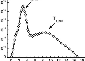
electron populations, a low-energy population (called cold electron population) and a high-energy population (called hot electron population). Usually the average temperatures of the cold and hot electron populations, denoted as _ and _ respectively, are used as the representative and characteristic parameters for the respective populations. An example of such an EEDF from a C-HiPIMS discharge is presented in Fig. 3.
Figure 3. An EEDF from a Ne-HiPIMS discharge of carbon, showing two distinct electron populations (cold and hot). The EEDF was obtained by performing Langmuir probe measurements (see Sec. 5.11).
From such an EEDF, the electron density ne can also be determined. Te and ne in a plasma discharge are dependent on the type of the buffer gas used, chamber geometry as well as process parameters and can be affected by for example, sputtered material vapor and presence of a reactive gas (such as O2, N2, C2H2). In the following sections, a brief
discussion on the effect of the gas atmosphere on the ionization processes with respect to changes in ne and Te is presented.
0 2 4 6 8 10 12 14 16 18 20 0 1x10 15 2x10 15 3x10 15 4x10 15 5x10 15 6x10 15 T e_hot Energy (eV) I n t e n s i t y ( a r b . u n i t ) T e_cold
11
2.3 Plasma properties and gas composition
2.3.1 Effect of change of buffer gas
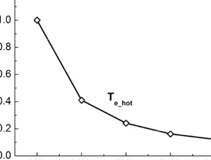
Owing to different ionization/excitation energies and cross sections, different ne and Te result from using different buffer gases. Eiz of the buffer gas sets the Te in a plasma discharge [27]. Higher Eiz buffer gas such as Ne provides a higher Te as compared to commonly used Ar, given that ne is the same (a larger power will be required in order to produce the same ne using Ne as with Ar) [27]. Higher Te means an increased ionization efficiency in discharges where electron impact ionization is the dominating ionization mechanism (high plasma density discharges such as HiPIMS) [28]. In paper I, plasma properties of C-HiPIMS discharges were investigated under different gas atmosphere by measuring ne and Te. The gas atmosphere consisted of a mixture of Ar and Ne where Ne content was varied to analyze the influence of change of Eiz on ne and Te. Fig. 4 shows the results from the study where electron temperatures from cold and hot electron populations (see Fig. 3) are found to increase with an increase of the Ne content in the gas mixture.
Figure 4. Electron temperatures (Te_hot and Te_cold) from a C-HiPIMS discharge
containing Ar+Ne gas atmosphere as a function of the Ne content of the mixture. The electron temperatures were measured by employing a Langmuir probe. 0% 28% 50% 71% 83% 0.50 0.52 0.54 0.56 0.58 0.60 2 3 4 5 6 T e_cold T e_hot E l e c t r o n T e m p e r a t u r e , T e , ( e V )
2.3.2 Reactive gas atmosphere
In plasma-based thin film deposition, gas atmosphere consisting of a reactive gas (such as O2, N2, C2H2) mixed with a buffer gas is commonly used, such as for compound thin film
deposition. The presence of a reactive gas brings about various interactions in addition to ionization; such as rotational and vibrational excitations, dissociation of molecular gaseous species etc. Depending on their cross sections and energy thresholds, these interactions can affect the ion generation by cooling down the plasma electrons. It has been shown that total energy losses per electron-ion pair created (which takes into account ionization, excitation as well as scattering interactions) for Te < 7eV (close to the
Te expected for bulk plasma electrons) are higher for O2 and N2 as compared to Ar [29].
The higher losses are attributed to losses due to dissociation as well as rotational and vibrational excitations. This suggests that the ion density in an Ar+O2 discharge is likely
to be lower compared to an Ar discharge. In an Ar+O2 discharge, the inelastic
interactions of plasma electrons with O2 will produce oxygen ions through direct and/or
dissociative ionization processes. Since Eiz of O2 (12.06 eV) [30] is lower than that of Ar
(15.75 eV) therefore oxygen ion generation is also expected. The reactive gas ion generation affects the plasma chemistry as well as discharge characteristics such as discharge current and discharge voltage are also influenced by the reactive gas ion fluxes (see sec. 3.4.2). These effects for reactive HiPIMS processes of Ti-O, Al-O and Al-Si-O have been investigated in paper V (Ti-O, Al-O) and paper VI (Al-Si-O).
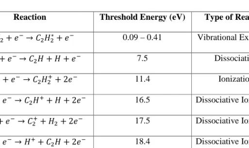
Mixing other reactive molecular gases such as hydrocarbon precursor gases (e.g. C2H2)
with an inert gas during the process of film deposition is likely to affect the discharge properties in a similar manner however; the plasma chemistry in this case is more complicated as compared to for example Ar+O2 discharge. Considering electron impact
induced excitation, dissociation and ionization of hydrocarbon species (here we take C2H2 as an example), various reactions resulting in different product species are possible
[31]. These reactions along with their threshold energies are outlined in Table I. Eiz (11.4 eV) of C2H2 is lower than Ar while its electron impact ionization cross section is about
twice as higher (24x10-17 cm-2 at 25 eV) [30] therefore large amounts of C2H2+ ions are
expected in the discharge. Also, the dissociation and dissociative ionization interactions result in the H generation therefore these discharges are abundant in atomic H. In paper
13 II, the discharge characteristics of an Ar+C2H2 discharge and its influence on a-C film
growth are investigated by assessing the structural properties of the resulting films. In Sec. 2.3.1 the effects of change of buffer gas on the plasma parameters were discussed where it was shown that replacing Ar with Ne increases the Te in the discharge (Fig. 4) which in turn enhances the ionization efficiency of the sputtered C. In hydrocarbon based discharges such a change of buffer gas, is likely to enhance the ionization as well as dissociation and vibrational excitations of hydrocarbon molecules. From the discharge properties as well as film growth perspectives, the change of plasma chemistry may become significant. This effect of change of buffer gas on discharge characteristics and a-C film properties is investigated in paper III by using Ar/Ne+a-C2H2 based HiPIMS
discharges.
Table I: Commonly observed electron impact induced reactions along with their threshold energies in low-pressure C2H2 containing plasma discharges.
The first ionization thresholds for Ar, C and H are 15.75, 11.26 and 13.59 eV, respectively [31].
Reaction Threshold Energy (eV) Type of Reaction
+ → ∗+ 0.09 – 0.41 Vibrational Excitation + → + + 7.5 Dissociation + → + 2 11.4 Ionization + → + + 2 16.5 Dissociative Ionization + → + + 2 17.5 Dissociative Ionization + → + + 2 18.4 Dissociative Ionization + → + + 2 20.3 Dissociative Ionization + → + + 2 20.6 Dissociative Ionization
2.4 Ionization of the Sputtered Material
As we have discussed in previous sections, Te and ne, are important in establishing how the plasma constituents interact with each other. In the plasma chemistry many mechanisms are working in parallel, which means that these two parameters are also important in determining dominating reactions through which the ionization of the sputtered material occurs. In a sputtering plasma, the most common ionizing mechanisms for sputtered material are, direct electron impact ionization, electron impact ionization of excited sputtered atoms and the ionization via the interaction with excited sputtering gas atoms (also called Penning ionization). These mechanisms are respectively represented as [27],
where M and G respectively represent the sputtered and sputtering gas atoms.
Plasma discharges with high values of ne are dominated by electron impact ionization (processes in relation 2.4 and 2.5) while the low ne discharges are dominated by Penning ionization (process in relation 2.6) [27]. This is demonstrated in Fig. 5 for the sputtering discharge of Al using Ar [27].
M0 + e- M+ + 2 e-, (2.4)
M* + e- M+ + 2 e-, (2.5)
15
Figure 5. The process of ionization of sputtered Al at 36 mTorr of Ar gas pressure showing the region of dominance for electron impact and Penning ionization processes. (After J. Hopwood [27].)
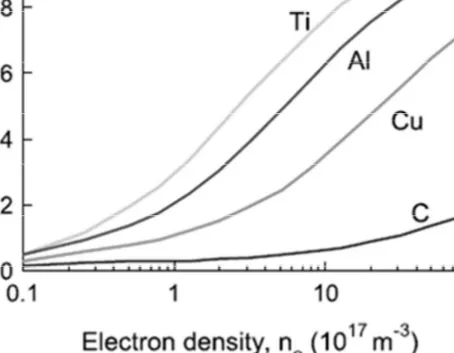
Fig. 5 also demonstrates that a higher ionized fraction for the sputtered material is obtained with increased ne. This is a general trend for sputtered materials however, the absolute number of the ionized fraction varies with the material dependent cross sections for ionizing reactions. Metals are readily ionized with ne in the range of 1016 to 1019 m-3 while the ionized fraction for non-metals such as carbon is low in this plasma density region. One of the factors for the low ionized fraction for the case of non-metals is their higher Eiz values as compared to metals (for example, Eiz for C is 11.26 eV while for Al it is 5.98 eV). The dependence of the ionized fraction of the sputtered material on the plasma density is demonstrated in Fig. 6 for various materials [27].
Figure 6. The ionized flux fraction dependence on plasma density for different materials. (After J. Hopwood [27].)
The dependence of the degree of ionization of the sputtered material on Te and ne can also be understood by looking at the mean ionization length of a sputtered atom, which is the average distance the sputtered atom travels before it is ionized in a plasma discharge [28]. For the electron impaction ionization, the mean ionization length (here denoted as λmiz) of the sputtered atom can be expressed as [28],
where vs is the velocity of the sputtered atom and kmizis the rate constant for electron
impact ionization which is expressed as,
(
)
miz vs k nmiz e λ = , (2.7)(
)
0 0 ( ) exp miz e e k T =k −E T . (2.8)17 The constants E0 and k0 are material dependent and they can be extracted from
experiments or computer simulations [28,32].
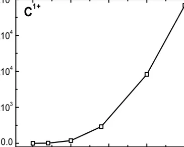
The exponential nature of kmizin Eq. 2.8 suggests that the degree of ionization of the sputtered material is more sensitive to changes in Te as compared to ne. As an example, the kmiz calculated using Eq. 2.8 for Te ranging from 1 eV to 5 eV and a constant value of
ne for C is presented in Figure 7. It can be observed that a change of Te from 1 eV to 5 eV increases the kmiz by about 4 orders of magnitude.
Figure 7. as a function of Te calculated for sputtered carbon using a
constant value of ne.
Eq. 2.7 shows that an increase in both, Te and ne will result in the decrease in the λmiz which implies that the probability of the ionization of the sputtered material will increase. In the light of this discussion, considering the results presented in Fig. 4 where an increased Te is shown to be obtained when increasing Ne content in the mixture of Ar+Ne
1 2 3 4 5 0.0 5.0x10 3 1.0x10 4 1.5x10 4 2.0x10 4 C 1+ N o r m a l i z e d I o n i z a t i o n R a t e C o e f f . Electron Temperature, T e , (eV)
in a HiPIMS discharge of C, it can be inferred that the sputtered C atoms will have lower mean ionization lengths in a Ne-based HiPIMS discharge as compared to Ar-based HiPIMS discharge. Using Te plotted in Fig. 4 and a constant value of ne in Eq. 2.7 through Eq. 2.8, the λmiz values are calculated for sputtered C. The result is presented in Fig. 8 which manifests about an order of magnitude decrease in λmiz and hence significant increase in ionization probability for sputtered C when the sputtering gas atomosphere is dominated by Ne.
Figure 8. of sputtered carbon as a function of Ne content of the sputtering gas mixture of Ar+Ne.
19
Chapter 3
Thin Film Deposition Processes
Thin film deposition in this thesis has been performed using magnetron sputtering based methods. In the following sections, a brief introduction of process of sputtering, magnetron sputtering as well as its relevant variants is presented. A section where thin film growth is discussed is also included.
3.1 Sputtering
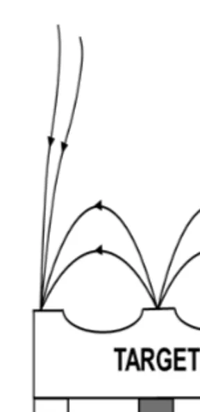
Sputtering is a physical process of ejecting target atoms (source material) by means of an incident energy and momentum transfer [1,2]. In a plasma-based sputtering process, the incident energy is supplied through collisions between the ions from the plasma and the target atoms. Ions from the plasma reach to the target surface under the influence of electric fields that are generated by applying a negative potential to the target. Upon the impact of the ions on the target surface, various ion-solid surface interactions occur. On the basis of the energy of the incident ions, the process of sputtering can occur in three regimes namely single knock-on (low energy regime, < 1keV), linear cascade (moderate energy regime, 1-50 keV) or spike (high energy regime, >50 keV). These interactions are depicted in Fig.9 [1].
Figure 9. Energy regimes of sputtering: a) Single knock-on (low energy), b) Linear cascade (moderate energy) and c) Spike (high energy). (Adapted from [33].)
The amount of source material sputtered from the target is dependent on the bombarding ion species, their energy and angle of incidence as well as target material. A relevant quantity that is used for expressing the relationship between these parameters is sputtering yield, Y, which is defined as [25]:
= !"# $% &'!(( ) ( ( ($"&
!"# $% * +*) ( *$ & (3.1)
For the energy range such as that valid for the process of sputtering (< 1keV), a linear relationship between the sputtering yield and the energy of the projectile is found to be a sufficient approximation. The sputtered target atoms follow the Thomson energy distribution whereas their spread can be approximated with a cosine distribution [34]. The sputtered atoms traverse through the bulk plasma and thereby condense onto all surfaces in the reactor. Through their course, the sputtered atoms suffer elastic collisions with background gas atoms and are subsequently thermalized [1,27,34]. A fraction of them can also be ionized due to the inelastic collisions with electrons as described in Sec. 2.4.
21 During the process of sputtering, besides the target atoms, electrons from the target surface are also ejected. These electrons are termed as secondary electrons [2]. The ejected secondary electrons are accelerated away from the target by the sheath potential (cathode sheath, see Sec. 2.2) reaching to the bulk plasma where they take part in the ionization of the sputtering gas atoms thereby helping the discharge to sustain. Similar to the sputtering yield, secondary electron emission is also dependent on the bombarding ion species and energy carried by them as well as on the composition of the target material. For low bombarding energy regime (<1 keV), secondary electron emission coefficient can be written as [35];
,-.= 0.032 (0.78567− 29) . (3.2)
Here ,-. is the ion induced secondary electron emission co-efficient, 567 is the ionization potential of the bombarding ion and 9 is the work function of the target surface. Eq. 3.2
has been deduced by fitting the experimentally determined secondary electron emission for various metals.
Figure 10. Schematic showing the concept of magnetron sputtering. Here G is representing an incident sputtering gas ions whereas M is the sputtered metal atom.
3.2 Magnetron Sputtering
Typically, the amount of ejected secondary electrons is low (,-. ~ 0.05 − 0.2 for most metals) [36,37] therefore to achieve an easier sustainability of the discharge it is desired that the ionization efficiency of the secondary electrons (ionizing events per electron) is enhanced [2]. This can be achieved by confining the secondary electrons in a region very close to the target surface. This is the principle of so-called magnetron sputtering, where the confinement of the electrons is achieved by using magnetic field (Fig. 10). This is commonly achieved by placing permanent magnets at the back of the target such that the magnetic field lines form a close loop thereby trapping the electrons. The effect of the electron confinement is the increased ionization efficiency and thereby an increased rate of sputtering. This also ensures an operation at reduced pressures as compared to diode sputtering where a high pressure is required to ignite as well as sustain a plasma discharge. The concept of a magnetron sputtering is illustrated in Fig. 10.
Figure 11. Schematic showing the balanced (left) and unbalanced (right) magnetic field configurations of a magnetron.
23 Two different magnetic field configurations — balanced and unbalanced — are employed for a magnetron, Fig. 11. In a balanced magnetic field configuration, the strengths of the inner and outer magnetic pole pieces are the same and the magnetic field lines form (virtually) close loops. Such an arrangement provides efficient confinement of the secondary electrons close to the target surface. In an unbalanced magnetic field configuration, the strengths of the outer and inner magnets are not the same. For instance in the so-called type-II unbalanced magnetron (as shown in Fig. 11), outer magnets are made stronger than the inner magnets. This allows the magnetic field lines to open-up and extend in the chamber towards the substrate. The secondary electrons will follow the field lines dragging also the gas ions along with them thereby extending the plasma close to the substrate. This provides possibility to promote ion bombardment at the substrate (for example by applying a substrate bias potential) during the film growth which is beneficial for example for modifying the film properties.
3.2.1 Direct Current Magnetron Sputtering
One of the most common magnetron sputtering based method which is widely employed for the synthesis of thin films is DCMS. In DCMS, the target material is vaporized by applying a constant power while keeping the target power density in the order of a few Wcm-2, which is necessary to prevent overheating of the target [7]. The resulting target current densities are in the order of a few mAcm-2 [8,38]. Such current and power densities provide plasma densities in the order of 1014–1016 m-3 [8]. The sputtered target atoms which typically have energies in the order of few eV with energy tails of several tens of eV are not ionized to large degrees due to low plasma densities. The resulting ionized fraction of the sputtered metals in DCMS processes is of the order of few percent [39] and the majority of the depositing flux consists of neutral species. This means that the energetic deposition conditions which are essential for the modification of the film properties are difficult to achieve. Furthermore, the film deposition proceeds as line-of-sight deposition and uniform film growth on complex-shaped objects is difficult. As discussed before, by employing an unbalanced magnetron and by applying large negative bias potentials to the substrate, ion bombardment during the film growth can be promoted [1]. However, since the ionized fraction of the sputtered material is low, mainly sputtering gas ions (for example Ar+ ions) are likely to reach to the substrate. For high
substrate bias potentials, this can lead to the implantation of the sputtering gas ions into the films which may deteriorate the film quality for example by introducing stresses in the films.
3.2.2 High Power Impulse Magnetron Sputtering
As we have discussed in the previous section, an increased ionized fraction of the sputtered material is desired for the modification of the growing film and tailoring the film properties. The ionized fraction can be enhanced by increasing the plasma density (as discussed in Sec. 2.4) which in turn is dependent on the target power densities. Due to the limitation of heat-load on the target, this cannot be achieved using a constant power, such as using DCMS. In HiPIMS large plasma densities are achieved by applying the a high power to the target in the form of short pulses (pulse frequencies in the range of 100 Hz to 10 kHz) such that the duty cycle (pulse on time between 5–500 µs) is kept low (<5%) to avoid overheating thereby preventing the target damage. This enables an operation with typical peak power densities in the order of several kWcm-2 and target current densities of the order of several Acm-2 resulting in plasma densities in the order of 1018–1019 m-3 which are 2–3 orders of magnitude higher as compared to DCMS [8– 10,20].
The HiPIMS process conditions have been shown to facilitate high degree of ionization of the sputtered metals (~90% for Ti) [40] as well as relatively higher energies of the sputter-ejected metal ions as compared to DCMS have been measured in HiPIMS processes [41]. High degree of ionization and energetic deposition fluxes have been shown to facilitate the synthesis of smoother and denser elemental and compound films with a control over their microstructure, phase composition, mechanical and optical properties [11,20,42]. Furthermore, uniform film deposition on complex-shaped substrate, improved film adhesion to the substrates as well as possibility of low-temperature synthesis of thin films has also been demonstrated by HiPIMS [12,21,43]. In this thesis, HiPIMS discharge characteristics and the effect of HiPIMS process conditions on the film growth have been investigated for elemental as well for reactively deposited compound thin films. A representative of the discharge characteristics of a HiPIMS process is its discharge current-voltage characteristic and many important
25 aspects of the discharge can be inferred by analyzing for example; the resulting peak target voltage, shape and peak values of current waveforms etc. Typical current-voltage characteristic curve from a HiPIMS discharge are presented in Fig. 12. Several authors have studied the discharge current-voltage characteristics during a non-reactive as well as reactive HiPIMS process [44–46]. Lundin et al. [44] have discussed the HiPIMS discharge characteristics by considering the discharge current in three distinct phases; (I) plasma ignition followed by (II) a decay after passing a current maximum and (III) a steady-state regime as seen in Fig. 12.
Figure 12. A voltage and current pulse recorded from a Ti Ar-HiPIMS discharge operated at 200 W of average power.
In the plasma ignition phase, initially the discharge current is constituted mainly by sputtering gas ions whereas the latter part of the phase is dominated by ionized sputtered atoms because a fraction of these may return back to the target (due to large applied negative voltages) and contribute to the discharge current. The decay after the peak current in the second phase occurs due to reduced gas density in front of the target. This is mainly caused by loss of sputtering gas atoms via ionization as well as due to
rarefaction via collisions from the sputtered material flux. The steady-state phase essentially reflects DCMS-like plasma density and heat equilibrium regime which is observed for pulse on time (ton) ≥ 200 µs.
The discharge current is essentially the sum of the ion and electron currents and it can be written as;
As discussed in Sec. 3.1, due to the ion bombardment on the target surface, emission of secondary electrons from the target surface occurs. These secondary electrons will also contribute to the discharge current. Therefore, the discharge current at the target surface can be written in the following form [47]:
where =6 > is the total ion current constituted by ionized species from the plasma. ,-., the secondary electron emission coefficient can be determined using Eq. 3.2.
The discharge characteristics of HiPIMS processes for carbon-based thin film growth have been investigated in paper III whereas for metal-oxide thin film growth, the investigations on the discharge properties are carried out in paper IV and V.
3.3 Reactive Magnetron Sputtering
Reactive magnetron sputtering refers to the magnetron sputtering based method of film deposition where the gas ambient consists of a reactive gas (such as O2, N2) that is either
used alone or mixed with an inert gas [2,34]. Typically, the method is employed for compound film growth such as Al-O, Ti-N etc. Different approaches are employed for compound film synthesis such as film deposition performed using a compound target in either a pure inert or reactive gas ambient or compound film deposition carried out using for example a metallic target in a mixed inert gas and reactive gas ambient [34]. An
=?= =6 >+ = @ >, (3.3)
27 example of the former is the synthesis of Al2O3 [48] thin films using an alumina target
sputtered in an Ar gas ambient and an example of the latter is the synthesis of TiO2 thin
films using a Ti target in a gas ambient of Ar+O2 [22]. In this thesis, the approach of
reactive sputter deposition has been employed for synthesizing a-C:H (paper II and III), Ti-O (paper IV) and Al-Si-O (paper VI) thin films.
During the process of reactive sputtering, a stepwise increase of the reactive gas flow into the process chamber initiates the formation of compound on all surfaces (target, chamber walls, substrate etc.) via chemisorption [49,50]. The compound formation depends on the reactive gas flow, surface coverage and the sticking coefficient of the reactive gas atoms. At the target surface, the compound formation is affected by the process of sputtering which will depend on the ion current density, sputtering yield of the compound as well as the target surface coverage [51]. Under low flow rates of the reactive gas, the target surface coverage by compound formation is small and the compound is over-sputtered by metal resulting in substoichiometric film growth at the substrate [49,51]. The partial pressure increase of the reactive gas in this condition is not significant. This mode is often referred to as metallic mode. At very high flow rates where the target surface is completely covered by the compound (poison/compound mode), the resulting films are stoichiometric however, owing to the low sputtering yield of the compound, low deposition rates are often observed. In the poison mode, there exists a linear relationship between the partial pressure of the reactive gas and the gas flow rate [49].
The transition from the metallic to compound mode is often abrupt and any operation within the transition zone is likely to result in an unstable process as well as hysteresis in the process parameters such as partial pressure of the reactive gas. The advantage of running at the transition zone is that stoichiometric thin films can be synthesized at higher deposition rates as compared to the compound mode. Process stability at the transition zone can be attained by controlling the target surface coverage i.e. reactive gas flow by employing a feedback system. Several methods are used that allow for controlling the reactive gas flow by monitoring for example the partial pressure of the reactive gas, discharge voltage or optical emission from the discharge [52].