A wishbone compatible SD card mass storage controller
for
embedded usage
Master’s Thesis at Mälardalen University
2009
Adam Edvardsson
Thesis Supervisor: Fredrik Ekstrand
Company Supervisor: Michael Unnebäck
Abstract
The purpose with this thesis was to develop an open source SD card controller IP core for usage in small embedded system, emphasis has been laid on using as few logic gates as possible, providing an easy user interface and making it viable as a system disk controller.
For the most part, the lack of a complete open SD specification has mainly affected embedded systems, since desktop users generally read SD cards via USB-based card readers. But recent openings of the SD specification have made it possible to develop SD-card readers which are utilizing the SD bus protocol.
Implementation has been done in Verilog for the hardware parts, and the software was developed in C. The proposed design has features common in disk controllers, like direct memory access, interrupt generation, and error control.
The design uses approximately 4000 core cells and 2 RAM blocks, about 50% less logic then a commercial alternative (Eureka EP560 ). Also a second smaller core was developed by making few modifications of the full design, thereby showing the strength of a freely modifiable open IP core.
Glossary
SD: Secure Digital
SDHC : Secure Digital High capacity
ASIC: Application-Specific Integrated Circuit, integrated circuit,customized for a particular use BD: Buffer Descriptor
CRC: Cyclic Redundancy Check, a error detection algorithm
DMA: Direct Memory Access, access of system memory independently of the central processing
unit.
FIFO: First In First Out buffer, refers to the way data is stored in a queue.
FSM: Finite State Machine, a model of behaviour composed of a finite number of states,
transitions between those states, and actions.
FPGA: Field Programmable Gate Array, a reprogrammable semiconductor device. HDL: Hardware Description Language
IP core: Intellectual Property Core, a reusable unit of logic, cell, or chip layout design
MMC: Multi Media Card
MMU: Memory Management Unit, a computer component responsible for handling memory
accesses requested by the CPU
ORPSoC: OpenRISC Reference Platform System-on-Chip REQ: Request Signal
RX: Receive
SOC: System On a Chip, integrating all components of a computer or other electronic system into
a single integrated circuit
SPI: Serial Peripheral Interface Bus, Limited to 1 data channel in SD card. TX: Transmit
UFD: USB Flash Drive, a data storage device integrated with a USB interface
Bit Abbreviations.
S: Start bit (= ‘0’)
T: Transmitter bit (Host = ‘1’, Card = ‘0’)
P: One-cycle pull-up (= ‘1’ (active driven by card or host)) E: End bit (=1)
Z: High impedance state ( -> = ‘1’ (driven only by pull-up resistors)) D: Data bits
X: Don’t Care data bits (from card)
Notations
italic style is used to indicate: code, types, module and function names.
Context
1. INTRODUCTION...1
1.1 BACKGROUND...1
1.2 PURPOSE & GOALS...1
1.3 METHOD...2 2. BACKGROUND...2 2.1 SD CARD...2 2.1.1 SD ARCHITECTURE...3 2.1.2 SD BUS...4 2.1.2.1 SD BUS PROTOCOL...4
2.2 SD CARD OPERATIONMODES...4
2.2.1 CARD IDENTIFICATION MODE...5
2.2.2 DATA TRANSFER MODE...5
2.2.2.1 DATA WRITE...6
2.2.2.2 DATA READ...6
2.2.2.3 MULTIPLEBLOCKOPERATION...6
2.2.2.4 PRE ERASE...6
2.3 SYSTEMON CHIP...6
2.3.1 IP CORES...7
2.3.1.1 DATA TRANSFER MODE...7
2.3.2 OPENRISC CPU CORE...7
2.3.3 WISHBONE BUS...7
2.4 LINUX...8
2.4.1 OVERWIEV...8
2.4.2 DEVICE DRIVERS...8
2.4.3 BLOCK DEVICESDRIVERS...8
2.4.4 SD CARD DEVICESDRIVERS...9
2.5 STATEOFTHEART...9
2.5.1 SD CARD...10 2.5.2 USB FLSH DRIVE...10 2.5.3 COMPACTFLASH...11 2.6 RELATED WORK...11 2.6.1 COMMERCIAL...11 2.6.2 OPEN CORES...12 3. METHODS...12
3.1 GENERALDESIGNCONSIDERATIONS...12
3.1.1 CLOCKDOMAINS...12
3.1.1.1 FIFO...12
3.1.2 FSM...12
3.2 DEVELOPMENT TOOLS...13
4. HARDWARE DESIGN AND IMPLEMENTATION...14
4.1 HOSTINTERFACE...15
4.1.1 CONTROLLERWBMODULE...15
4.1.2 CLOCKDIVIDERMODULE...15
4.2 CARDINTERFACE...15
4.2.1 CMD MASTERMODULE...15
4.2.2 BUFFER DESCRIPTORMODULE...16
4.2.3 DATA MASTERMODULE...16
4.2.4 BUFFERFILLERMODULE...17
4.3 PHYSICAL INTERFACE...17
4.3.1 CMD SERIALHOSTMODULE...17
5 SOFTWARE DESIGN...20
5.1 STANDALONEPACKAGE...20
5.2 LINUXDRIVER...20
6 VALIDATION AND TESTING...21
6.1 HARDWARE...21 6.1.1 UNITTESTING...21 6.1.2 INTEGRATIONTESTING...21 6.1.3 TESTBENCH...22 6.1.4 SYSTEMTESTING...22 7 RESULT...23 7.1 SYNTHESIS...23 7.2 WRITEPERFORMANCE...23 7.3 READPERFORMANCE...23 8 FUTURE WORK...24 9 CONCLUSION...25 10 REFERENCES...26 APPENDIX...27 A. SD-CARD...28
A.1 CARDSTATEDIAGRAMINCARDIDENTIFICATIONMODE ...28
A.2 CARDSTATEDIAGRAMINDATATRANSFERMODE ...29
A.3 MULTIPLEREADOPERATION ...29
A.4 MULTIPLEWRITE OPERATION ...30
B RELATED IP CORES...30
B.1 EP560 SD/SDIO/MMC SLAVE CONTROLLER ...30
B.2 SD 2.0 COMBO DEVICE IP A...31
B.3 OPENCORES SDC 2.0 DMA...32
C TESTCASES...33
D. COREDETAILS ...35
D.1 LISTOF REGISTERS...35
D.2 AVAILABLE COREOPTIONS ...37
D.3 CORE IO PORTS ...38
List of figures
Figure 1: SD Card Architecture ...3
Figure 2: Timing for Block Write...6
Figure 3: Timing for Block Read...6
Figure 4: Wishbone Standard connection...8
Figure 5: System call Linux...9
Figure 6: Layers of the SD-card driver in Linux...10
Figure 7: Synchronizing of an asynchronous input...12
Figure 8: Components of a FSM...13
Figure 9: Overview hardware design...14
Figure 10: FSM CMD master...15
Figure 11: FSM Data master...17
Figure 12: Timing handshake...18
Figure 13: FSM CMD Serial Host...18
Figure 14: FSM DATA Serial Host...20
Figure 15. Logic analyser output...22
Figure 16. Test bench...22
Figure 17. Logic analyser output for write block...23
Figure 18: Logic analyser output for read block...24
List of tables
Table 1. SD Card registers...4Table 2: Command token...4
Table 3: r1,r3,r6 response token...4
Table 4: Card state and Host Operation modes...5
Table 5: EP560 Device utilization ...11
1 Introduction
1.1 Background
This work has been carried out at Mälardalens Högskola in cooperation with the company
ORSoC. ORSoC is an ASIC design and manufacturing services company. They are also managing the project opencores.org [1], which is a digital open source hardware community with the
objective to design and publish core designs under an open license: Lesser General Public License (LGPL).
The biggest drawback with commercial IP cores are that they often come in the form of pre compiled blocks, so called generic gate net lists. This means that they cannot be modified to suit new standards or meet special needs. An open source IP core however, can freely be modified to suit new standards and special needs.
Memory cards have for a long time been a popular storage medium for consumer electronics such as cameras, mp3-players and cellphones. The reason for its popularity is a combination of factors, like the small form factor, the high data density and the good power saving capability. But using SD cards in smaller projects, like hobby and school projects has been a bit tricky. Either you had to use an external SD controller chip or the slower but easy to use SPI mode, because commercial IP SD controllers are very expensive and might not suit your needs.
Lately the SD license has been opened up and parts of the specification has become free, so now it is possible to make an open core SD controller that uses the 4 bits bus protocol. This proposed implementation of an SD controller will further encourage the use of the SD-card, particularly for embedded applications.
1.2 Purpose & Goals
The purpose of this thesis work was to design and implement an open source Wishbone compatible SD card mass storage controller for an FPGA, together with a software wrapper.
The SD controller was meant to be used in the reference design of an SOC (ORPSoC) and will there operate as the controller for the system disk. Therefore emphasis was put on making a design with features a system with an operating system (Linux) will benefit from. The SD bus protocol was to be used, to utilize the speed capacity of the card to the maximum.
The work was divided into packages. Package 1 is mandatory and defines the actual controller. Package 2 is a software wrapper.
The general requirement was that the SD controller should use the 4 bit SD-bus protocol and that the implementation should be written in Verilog. The implementation should also be compatible with Wishbone revision 3B and be technology independent. Technology independent in this context meant that it should be free from specific vendor technologies.
Work package 1 1. Study SD protocol
2. Write a requirement specification 3. Implement functionality in Verilog
4. Verify behaviour in simulation environment (using SD card HDL model if available) 5. Verify behaviour on existing development board
Work package 2
1. Implementation of software wrapper in C
2. Optional implementation of software support for file system (FAT16 and or FAT32) Work package 3
1. Implementation of SDIO protocol
1.3 Method
The goal has been accomplished by literature studies and supervisor advices.
To get a grasp about what should be done and how similar controllers operates, a pre study phase was necessary where the SD Specification Physical Layer [2] documentation and features of common consumer disk controllers [3] was studied .
To learn the HDL language Verilog, the Verilog tutorial [4] was followed. Some more advance tips about Verilog coding was found in the “ The Ten Commandments of Excellent Design”[13] ,
verilog_manual [5] and opencores design guide [6]. Other documents read in this phase was about
how to write FSM [8] and asynchronous FIFO [9].
To be able to create an optimized controller as well to prevent walking into as few pitfall as possible a deeper knowledge in certain areas was required. As an IP core it should be suitable for different kinds of system, but the key aspect was to optimize it for the ORSoC System. Therefore also some effort was put into getting knowledge of theirs system as well. For this Wishbone specification [7], SD Specification Physical Layer [2], OpenRISC architecture [16] and Linux device drivers [10] was read with the following question in mind:
1. The SD card: How does it work, what features do we have and how to maximize the performance ?
2. Linux: How do drivers work and how can we increase the performance with hardware?
3. The system (SOC): How does the bus work, how to maximize the speed and what features does the CPU have?
An incremental development method was used, where small part of the design was implemented ,tested and verified before new features were added. Once that was done the design was expanded with a new small part and retested. By testing the parts of a program first and then testing the sum of its parts, integration testing becomes much easier .This method has the benefit of detecting bugs and problems early and you get more control over the design. However the drawback is that when adding features to an already tested part, retesting of all parts who use this part might be needed.
design are provided.
2.1 SD Card
During the last 10 years, the sales of cellphones, digital cameras and mp3 players have been
exploding. The needs for convenient data storage for small hand-held devices have been increasing in the same way. The flash memory card was introduced to the market to meet the requirements of a small storage media, with big storage capacity.
The Multi Media Card (MMC) was one of the cards that emerged in this era (1997) , the reason for its success was its small form factor and high data density as it used the NAND-Flash technology. In the late 1999 a group of consumer electronic companies ( Panasonic, SanDisk, and Toshiba ) went together and developed the Secure Digital card standard which is an extension of the MMC. By doing this the bus width was increased to four bits and the physical size became twice as thick. The storage space and transfer speed was hugely improved, storage capacity was limited to 2GB and the transfer speed limit was 25Mbit/s.
2.1.1 SD Architecture
Figure 1 shows the architecture of the SD card, the external interface consists of 9 pins, the location of them can be seen in the same picture.
For the SD-bus mode the interface consists of four data pins DAT0-DAT3 and one command pin CMD. The signals on those pins are bi-directional, and they are operating in a push-pull mode between the host and card (Signal can be driven from either end, with better timing then open-drain). Then there is one CLK pin for the clock signal. The rest of the pins are for VDD voltage supply and VSS for grounding. Internally the SD card consists of an interface driver, card interface controller, a set of registers (Table1), a memory core interface and the flash memory. Modern cards also have internal data buffers. The interface driver is forwarding the CMD and DATA signals to the card interface controller. The card interface controller decode the incoming CMD signals and perform the specified task. A subset of the tasks is to
write/read data to the registers and fetch or write
data to the flash memory. Figure 1. SD Card Architecture [2]
The controller is also responsible for error detection and correction. More advanced models have advance wear levelling algorithms, which is a method to increase the life span of the product. This is done basically by remembering which block that has been erased recently, to be able to do this you first have to separate logical blocks (blocks requested) from physical blocks
Name Width Description
RCA 16 Relative card address; local system address of a card, dynamically suggested by the card and approved by the host during initialization
DSR 16 Driver Stage Register; to configure the card’s output drivers CSD 128 Card Specific Data; information about the card operation conditions
SCR 64 SD Configuration Register; information about the SD Memory Card’s Special Features OCR 32 Operation conditions register
SSD 512 SD Status; information about the card proprietary features CSR 32 Card Status; information about the card status
Table 1. SD Card registers [2] 2.1.2 SD BUS
The SD bus consists of the pins described in previously section. 6 communication lines and three supply lines. To the DATA and CMD communication lines pull-up resistors have to be connected, to avoid floating of the bus when in tristate and when having a disconnected card.
2.1.2.1 SD BUS Protocol
There are two types of communication over the SD bus, command and data transmission, using the CMD line and the DAT line. A command transition is initialized by pulling the CMD line low, and a data transmission is initialized by pulling DAT0 line low.
A command is a token which starts an operation in the SD card, and in response to a command a response token is sent by the card (as long it is not a reset command). Table 2 shows the format for a command token. There are 4 different response tokens r1 (normal response), r2 (CID or CSD register), r3 (OCR register),r6 (Published RCA response). Table 3 shows the format for r1,r3 and
r6 response. The r2 response format is the same, with the only difference that the content is 128 bit
and therefore a 136 bit wide response token is used for r2 type.
Bit Position 47 46 [45:40] [39:8] [7:1] 0
Width (bits) 1 1 6 32 7 1
Value 0 1 X X X 1
Description Start Bit Transmission bit Cmd index Argument CRC7 End bit
Table 2: Command token [1]
Bit Position 47 46 [45:1] 0
Width (bits) 1 1 40 1
Value 0 0 1
Description Start Bit Transmission bit Content End bit
Table 3: r1,r3,r6 response token [1]
Data transmissions are done in block and can be configured to use multiple data lines. Data transmissions are always proceeded by a CRC-16 checksum for each data line. Data is sent in two ways depending on the type of data, either usual data, or wide width data. Usual data is sent with the least significant byte to most significant byte where in each byte the most significant bit to least significant bit sequence is used. For wide width (Status register SSR) data is shifted from the
2.2 SD Card Operation modes
To get the card to “boot” into SD mode the host has to pull the CMD line high for at least 74 clock cycles. The SD card has 10 predefined states, and the host operates in 3 modes, as seen in table 4.
Card State Operation Mode
Inactive State Inactive Idle State
Card identification mode Ready State
Identification State Stand-by State
Data transfer mode Transfer State
Sending-data State Receive-data State Programming State Disconnect State
Table 4: Card state and Host Operation modes [1]
2.2.1 Card Identification Mode
In this mode the host initializes the card, the goal of this state is to validate if the card and host are compatible. Also the host will know what kind of card it is communicating with -SD, SDHC, SDIO or MMC card. The difference between the cards are in how they respond to the commands in the identification mode. All the communication in this mode is performed on the CMD line. The state transition diagram for all card states can be found in appendix A.1- A.2
At start of the identification process the card should first be reset, which is done by sending it a reset command,. This is done to be sure that the card is in idle state. When the card is in idle state is is ready for receiving commands. In the next step the interface condition is validated. To validate the interface condition, the host sends its voltage operation range to the card. The card responds only if it is specification 2.0 compatible and if the voltage operation is valid for the card. If no response is received the host know that it is either a 1.0 card or an operation condition mismatch, with an operation mismatch to be discovered with the next command in the chain. However, if a response is received the host knows that it is a 2.0 card and additional features can be enabled. A received response is validated with CRC check and bit matching, an invalid response will put the card to inactive state.
Next command specifies the operation condition to the card, this command has two purposes: the first is to specify the required operation voltage window, the second is to check if the card is busy. A card with an incompatible voltage windows should discard itself from further bus operations and no response will be delivered. When a response of the operation condition is received it checks for a busy bit in the response data field. If the busy is set the operation command is resent until the busy bit is cleared, then the host know the card has finished its start-up operations. The content of the response also indicates if a card has compatible operation conditions, the HCSD cards also reply with a CCS bit in the response, letting the host now it is a high capacity card.
The host then asks the cards for their CID register, which is unique for all cards. The final command in the initialization sequence is the request of RCA which is the address of the card, which will be used when addressing cards in the data mode.
2.2.2 Data Transfer Mode
After the identification mode the card will be in the idle state if everything went well. To set the card to transfer state one additional command containing the RCA number is sent, card with matching RCA number will then be put in transfer state. Before transmitting data there are some settings that should be set, like the data width which can be set to 1 or 4 bit and the block length that can be set to a value between 1 and 2048 (fixed to 512 for HCSD card).
2.2.2.1 Data Write
To write data to the card either a single block or a multiple blocks command can be used. The basic timing for the single block write is shown in figure 2 (for explanation of the bit abbreviation see glossary). First the command is sent, and a response is received after Ncr (2-64 cycles). When the host has received the response, the data transfer can begin after a minimum of Nwr (2) cycles. The format of the data is as described in section 2.1.2.1. After a data transmission, the card replies with a 3-bit CRC status token, this always occurs 2 cycles after the end bit.
“010” indicates a successful transfer (no CRC error). In case of CRC error the card response with “101” and no data will be written to the card. After a data write the card can become busy if its write buffer is full. If that is the case the DAT0 will be kept low until ready again.
Figure 2: Timing for Block Write [2] 2.2.2.2 Data Read
The reading of data is performed in a similar manner. First a read block command is sent, the host should then be prepared that data can arrive at any moment. The card starts to send data NAC cycle after receiving a data read command, Nac(max)= 100 ((TAAC * fpp) + (100 * NSAC)); TAAC and NSAC are card specific delay values, which can be found in the CID register.
Figure 3: Timing for Block Read [2]
2.2.2.3 Multiple block operation
There are also one transfer mode where there is no need to issue a command for each block to be sent. Instead just the address of the first block is sent, then the card transfer data until a special stop command is received. Timing and more information about those commands can be found in appendix A.3-A.4
2.2.2.4 Pre Erase
The flash memory requires an erase before it can be written to it. By issuing an erase command before a multiple block write, the card starts to erase blocks during the time it receives data . In normal operation, the SD card erases the flash just before writing to it.
2.3 System on Chip
In a system on chip you take the concept of microcontrollers one step further, instead of just integrating a computer on a chip you integrate an entire system. The opencores SoC reference design ORPSoC [16] (which will be used in the project) consist of a openRISC CPU, Ethernet controller, USB controller, SDRAM controller, UART and JTAG debugger.
2.3.1 IP cores
The SOC is composed of separate building block called IP cores. IP cores has a well specified interface, often towards a bus for easy integration with the existing system. The usage of IP cores greatly decrease the development time of systems, as they are tested and verified.
IP cores used for SOC and FPGA development is called soft cores (defined at a higher level than gate level). However, most of the commercial IP cores just offer the gate net list, i.e., you cannot edit or in any way see how the core is built. This is a drawback because the core cannot be optimized for your target system, and you will become bound to that core for your system.
2.3.1.1 Open cores
The opencores.org community offer user developed IP cores under some free license, such as LGPL and GPL. Here, all cores come with RTL code either described in Verilog or VHDL. The benefits with these cores are that they can easily be modified and optimised to suit your system. They are also often tested by many users which increases the chance that bugs are detected. The drawbacks are that no support is offered, and the quality cannot be ensured.
2.3.2 OpenRISC CPU core [18]
The openRISC CPU is a softcore with a Harvard 32 bit RISC architecture. Some of its features are integrated MMU, integer pipeline, data and instruction cache. The core is configurable, as an example, the MMU can be set to different page sizes, the cache can be set to between 0-8 Kb, hardware multiplication/division support can be added as well. The data order is fixed to big-endian.
The CPU offers 32 general purpose register as well as custom instructions. A memory operand is naturally aligned. The CPU has support for 32 Interrupt signals. A special feature is a power management register that, can be used to reduce power usage and even put it in hibernate mode.
2.3.3 Wishbone Bus
The WISHBONE interconnect is intended as a general purpose interface. As such, it defines the standard data exchange protocol between IP core modules [19] . It is not a physical bus in the sense of a PCI or ISA bus, as it does not specify electrical information or the bus topology. The core is instead implemented in the system as logic.
The bus can have multiple master/slave units, allowing multiple IP cores to control the same memory.
The bus is highly configurable. Address and data widths can be set between 1-64 bits, and it is capable of both little- and big endian transfer. Different interconnection schemes can be used as shared bus interconnection, point to point connection and crossbar switches etcetera (Figure 4). An additional feature is the support for burst read and write, were multiple data block is transferred without individual acknowledgement of each data. Tagged signals can be added to extend the functionality of the bus.
Figure 4: Wishbone Standard connection [7]
2.4 Linux
This section will explain some basic concept behind the Linux kernel and continue with specific details important for the work.
2.4.1 Overview
The Linux kernel is divided in two parts, one user space and one kernel space. User applications are executed in the user space, the user space has to call the kernel (by software interrupt) to get access to hardware or other resources. Processes in the user space are memory protected as each user space has its own virtual address space.
In the kernel space the kernel and drivers reside, and they have unlimited access to hardware and all memory, thus allowing them to access functionality from other kernel space applications. Figure 5 describes the steps required for a user application to perform the read call read(int fd,
void *buf, size_t count). The transition between user space and kernels space is costly, the CPU
has to save all its registers and perform a context switch.
2.4.2 Device Drivers
A device driver is a software layer that lies between the applications and the devices. Almost everything in Linux is treated as files, this also applies to device drivers. Users communicate with device drivers through device files. Mainly there are two kinds of devices, character and block devices. A character (char) device is one that can be accessed as a stream of bytes. Because of all devices is treated like files, there are common driver interface and operation a device needs to provide. The required operations are: open device and close device, read device and write device.
Figure 5: System call Linux [14] 2.4.3 Block Devices drivers
A block device is an device that can mount a file system.
Efficient block drivers are critical for performance, and not just for explicit reads and writes in user applications. Modern systems with virtual memory work by shifting unneeded data to secondary storage, which is usually a disk drive.
The operations a block driver should support is a bit different from a char driver. The open and release operation is still needed and work on the same way (set the state of the driver and hardware accordingly). There are no functions that actually read or write data. In the block I/O subsystem, these operations are handled by the request function. This function is where the real
work ia done, or at least started.
The block driver request method has the following prototype:
void request(request_queue_t *queue) This function is called whenever the kernel believes it is
time for your driver to process some reads, writes, or other operations on the device.
2.4.4 SD card Devices drivers
To the 2.6 Linux kernel there are block device drivers available for SD-controllers, thus providing a good framework for developing new drivers. However, no documentation is available but
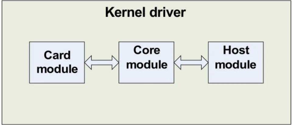
through investigation of the source file it is possible to see how it works. The driver consists of three modules, called core, card and host (figure 6).
The card module is the block driver as described in previously section, which initiates structures and provide the functionality for the queue and request methods. However, the commands is just dispatched and are handled by lower layers of drivers.
The host module takes care of the vendor specific communication with the SD-controller. This layer is the interface toward the card and takes care of operations like sending data and command. The module just write raw data into the structs leaving the decoding to higher levels.
However, the host module has not direct access to the card module, in between there are a core module which takes the raw data the host module generates and puts it into the correct registers.
Figure 6: Layers of the SD-card driver in Linux
2.5 State of the art
The need for a storage medium with big storage capacity, high transfer speed and low power consumption is increasing rapidly.
2.5.1 SD-Card
The SD-card was designed for small embedded systems, so a good energy saving support and protection for data corruption are built-in into the design.
Since the first product was released in the beginning of 2000, several improvements have been done. In the first draft 1.0 and 1.1 the card was specified to operate in range of 400Khz-25Mhz, giving a theoretical maximum transfer speed of 100 Mbit/s. Accessing data was done in a byte type manner, limiting the theoretical storage to 231 bytes or 2GB.
In 2006, the 2.0 of the specification was completed and the SDHC was introduced, now specified to clock speeds up to 50Mhz [2] increasing the theoretical speed to 200 Mbit/s. Also the addressing methods changed from byte to block addressing fixed to 512 bytes, there by increasing the
maximum data storage to 32GB.
In the beginning of 2009 the next generation of the SD card specification was announced:
SDXC[15]. From the press release it says that the theoretical maximum bus interface speed will be up to 832 Mbit/s with storage capacity of 2TB. To reach this transfer speed a clock speed at about 100Mhz will be required.
Kernel driver
Card module Core module Host module2.5.2 USB Flash drive
The USB flash driver was introduced in the beginning of 2000 [17], the basic principle behind it is the same, a flash controller and NAND-flash memory integrated on the same board. The transfer speed was initially limited by the USB protocol version 1.0 where the maximum transfer speed was limited to around 8 Mbit/s. However, with the introduction of USB 2.0 in the middle of the year 2000, speeds up to 480MB/s removed this limitation for newer UFD.
The storage capacity and transfer speed is keeping up with SD card pretty well. Modern UFD is often rated for speed at 200 Mbit/s. The drawback however with the UFD is that its not developed for embedded systems and therefore the form factor is bigger, and the power consumption is higher.
2.5.3 Compact Flash
Another competitor to SD card is the Compact Flash card, which has been on the market since 1994. It has lost market to the SD/MMC cards because of its bigger form factor, however it still managers to stay in the game. Even new versions are developed, today specification v 4.1 is available, which support 1064MBit/sec and storage capacities up to 137GB. However, its big form factor, the requirements for more pins and a higher power consumption makes it less suitable for embedded systems.
2.6 Related Work
Se Appendix B for more raw data
2.6.1 Commercial Eureka EP560
Since founded in 1993, Eureka Technology has established itself as a leading reusable IP cores provider with customer base in the United States, Japan, and Europe. Eureka provides an SD SD/SDIO/MMC Slave Controller. The SD memory and SDIO controller IP core supports the latest version 2.0 specification, it also supports the Multi Media Card(MMC) standard and SDMA data transfer, high capacity cards (SDHC) and high-speed data transfer mode (50Mhz).The core handles the SD or MMC bus protocol without any user management needed. This core is interoperable with existing standard software drivers. The core is delivered as a net list.
Table 5: EP560 Device utilization
Arasan SD 2.0 Memory Controller IP
Arasan Chip Systems Inc. founded in 1995, is a leading supplier of Reusable Intellectual Property (IP’s) cores, semiconductors and electronic design services. The controller supports all the same standard features as the Eureka core. It also has a feature where it mirrors the OCR, CID, CSD, DSR, SCR, and RCA or the SD card. A quite unnecessary feature as this register is seldom read and can easily be done by a few commands. The core is deliver with RTL code so modifications are doable.
2.6.2 Open Cores Spi master
There are one open core SD controller but it just supports SPI mode, and no DMA support or interrupt generation. The “spi master” is an SD (Secure Digital) and MMC memory card controller with an Wishbone slave interface. The controller hides the complicated SD/MMC memory interface, and presents the user with a simple FIFO interface. The cores handles all aspects of card initialization. Spi master is capable of block read and write transmissions of 512 bytes. The maximum transfer speed is 24Mbit/s.
3 Methods
3.1 General design considerations 3.1.1Clock domains
Special care has to be taken when signals are crossing clock domains, as the design no longer becomes synchronous. This adds some complications like metastable states and problems with data reliability.
One case when the data might become unreliable is when two modules operating in different clock domains need to send data between each other. The receiver module then have to know when the data is stable and can be clocked in. Also the sender module have to keep the data stable until it is read. This can be solved by utilizing a handshake protocol.
The metastable state is a condition when a digital signal does not settle onto one of the predefined states within a specified time. During the time from the set-up to the hold time, the input of a flip-flop should remain stable; a change in the input in that time will have a high probability of setting the flip-flop to a metastable state. If a flip-flop gets it input from another clock domain it cannot be guaranteed that the set-up to hold time will not get violated
To reduce the chance a metastable signal propagate into the design, an extra synchronization step could be added to the input signal (Figure 7). The synchronization consists of two connected flip-flops, clocked with the same clock. This greatly reduces the risk that an metastable signal
propagates into the design. The risk with a metastable signal propagating into the design, is that it might put it into a failure mode.
Figure 7: Synchronizing of an asynchronous input [13] 3.1.1.1 FIFO
Another way to solve the occurrence of unreliable data, is to use an asynchronous FIFO [9]. An asynchronous FIFO refers to a FIFO design where data values are written sequentially into a FIFO buffer using one clock domain, and the data values are sequentially read from the same FIFO buffer using another clock domain, where the two clock domains are asynchronous to each other. The throughput is a lot higher then the handshake method but require more logic.
3.1.2FSM
present state and output logic. It is recommended in [8] that the sequential and output logic is put in 2 different clocked block, this will require less code and has a better synthesize result.
Figure 8: Components of a FSM [8]
All FSMs should use one hot state encoding (1 bit per state) style because there are plenty of flip-flops in an FPGA and the combinational logic required to implement a one hot FSM design is typically smaller than most binary encoding styles. Since FPGA performance is typically related to the combinational logic size of the FPGA design, therefore onehot FSMs typically run faster than a binary encoded FSM with larger combinational logic blocks[8].
3.2 Development Tools
This chapter describes both the development hardware and the tools used during the development of the SD controller.
The hardware platform used for system testing was the opencores HW development board [3]. The board is equipped with a ACTEL ProASIC3, A3P1000 FPGA. The HDL code was written in verilog.
Tools used:
Overall: Vwware to run Windows on a Linux platform Designing: Fizzim FSM design tool
Coding: Programmers notepad 2.0.9
Preprocessing: VPPP, VerilogPerlPreProcessor Simulation: Modelsim 6.4a student version Synthesise: Synplify 9.6
Place and Route: Actel designer 8.5 Logic analyser: Intronix Logicport
Documentation: OpenOffice, Office Visio, Dia
For the software, the opencores GNU toolchain was used. The programming language for device drivers are C and the compiler used is the GCC compiler. GDB was used for the debugging connected to a JTAG interface.
4 Hardware design and implementation
The SD/MMC controller IP Core consists of 14 modules, divided into three layer Host interface, card interface and physical interface. The main idea behind this is that one layer can be
interchanged without affecting the others. The Module and sub modules operations are described later in this section. An overview of the design and the relation between the modules can be seen in figure 9. For external interface and register description see appendix D.
Figure 9: Overview hardware design
The operation can be summarized as follows.
To send a command to the SD card, the user has to write to two registers command and argument, residing in the sd_controller_wb module. The first register specifies the settings for the command and the second specifies the arguments for the command. The cmd_master module receives a signal when new data is written to the argument register. The cmd_master then reads the user register and composes a 40 bits command. The cmd_serial_host then sends the command to the SD card and waits for a reply. When the reply has been received it is sent back to cmd_master which then performs the error checks. Finally the reply data is written to a user accessible register and status bits are set in the normal interrupt status register marking a command transfer success or failure.
To transmit data, the user writes to a buffer descriptor, here describing the memory address of the data and the block address in the SD card. The data master then uses the cmd_master to send a block write/read command to the card. The cmd_serial_host module notify the data_serial_host when a data transmission is about to begin. The data_serial_host takes care of the transmission of the data and buffers it to the TX or RX FIFO. When the transmission is complete the data master checks for transmission errors by checking status bits in the data interrupt status register, marking data transfer success or fail. Se appendix D for more information regarding those register
4.1 Host interface
The host interface layer connects the core to the Wishbone bus with both a master and slave interface. The master interface is used for storing the received data block to
the memory and loading the data that needs to be sent from the memory to the
SD/MMC card. The slave interface is used when the CPU wants to access the internal registers. Both interfaces are Wishbone revision B.2 compatible. Currently, only DMA transfers are supported for transferring the data from/to the memory.
4.1.1 Controller_wb module
This module manages the wishbone slave interface, it contains all the user accessible registers. The module decodes the wishbone signals, checks for a valid read or write cycle then uses the address to find out which register to access.
4.1.2 Clock_divider module
A simple clock divider that divide the input clock with multiples of 2. This module is optional, its required if a variable clock speed is desired.
4.2 Card interface
This layer is like the brain of the core, or the master unit. It is responsible for moving data from the host interface layer to the physical layer. This layer is also responsible for detecting and reporting transmission errors to the host interface. Towards the physical interface, this layer acts like a bridge between the two clock domains. For reliable communication a level sensitive handshake protocol was implementation between the command master and command host. The handshake protocol was chosen because of its simplicity and low requirements of logic gates. For the data an asynchronous FIFO was used for higher performance.
4.2.1 CMD master module
The SD CMD Master module synchronizes the communication from the host interface with the physical interface. Mainly it perform three tasks:
•Read a set of registers from the user accessible registers in the wishbone module to compose a 40 bit command messages to pass to the physical layer.
•Read response messages from the physical layer and forward it to the user accessible registers. •Keep track of the status of the CMD_serial_host module.
Figure 10: FSM CMD master
The module is made up of a FSM with 3 states (Figure 10).
enters the SETUP state. In the setup state the settings for the command to be sent is set, as well as the command vector. The command vector is the command index merged with the argument vector. In the EXECUTE state the module signals that a new command vector is available for transmission, after that it waits for response of the command before going back to idle.
4.2.2 Buffer Descriptor module
The transmission and the reception processes are based on buffer descriptors. A buffer descriptor in this case contains a 32 bit pointer to the memory address where data should be read from or written to. The other 32 bit declare the SD-card block address were to read from or write data to. Two sequential writings to this module is required to create one buffer descriptor, because of the 64-bit size.
4.2.3 Data Master module
The module is made up of an FSM consisting of 9 states. It starts out in the idle state where it checks if there are any new BD that needs to be processed. If so the module processes the BD in the GET_XX_BD state. Then it enters the SEND_CMD state where it generates a command to the card, this is done by setting up the command and argument register. If the command line is free the module sends the command and go to the RECIVE_CMD state and waits for a response. If the response is valid the module starts the DMA and goes to the DATA_TRANSFER state, if there is not a valid response, the CMD is resent again.
During transmission in the DATA_TRANSFER state the module keeps track if the FIFO buffers underflows or overflows. When the transmission is completed it checks for valid CRC and if everything is ok it goes back to the idle state.
If anything goes wrong during a transmission it enters an error state (STOP) and the module try to restart the transmission n times before giving up.
Figure 11: FSM Data master
4.2.4 Buffer filler module
This module works as the DMA, it is shuffling data between the FIFO and the system memory. During it operation it also keeps track of the status of the FIFO:s. The input to this module is a enable signal and the memory address for the memory buffer. No output is generated as long as the FIFO does not get empty or full.
4.3 Physical Interface
The physical interface layer is handling the transmission of commands and data to the SD card. As the higher layer components just send raw data, this layer have to add the required controls and error checking bits. It also keeps track of the busy state of the SD bus so no transactions will be started when the line is busy. All communication with this layer is done by handshaking and FIFO buffering, because of the clock domain crossing.
4.3.1 CMD Serial host module
The SD_CMD_ serial_host module is an interface to the external SD /MMC card. It is used to read and write commands to the SD/MMC card. The external interface consists of two signals, clk and a bidirectional signal CMD. The cmd_out_o, cmd_dat_i and cmd_oe_o signals have to be combined in an additional module (Preferable the SoC top module).
Figure 12. Timing handshake
The data in and the data out from this module, cross a clock domain. Therefor are those signals synchronized with REQ and ACK signals, as seen in figure 12. REQ_IN is set to high when a service is requested, the module answer with setting ACK_OUT to low. As long as ACK_OUT is high the SETTING_IN and CMD_IN should not change. ACK_OUT is kept low until a CMD cycle is completed. When the Module has data to send ( like updated STATUS or valid data in CMD_OUT) the module assert REQ_OUT and wait for ACK_IN to go high before doing any further operations.
The module is built up on a FSM of 10 states, the states and transitions can be seen in figure 13. It starts out in the INIT state where it performs the SD card initialization sequence. This state only runs when the core is either soft or hard reset. It then stays in IDLE state until a write command arrives from the card interface layer. Depending on if it is a command with response or without response the next state will either be WRITE-WR or WRITE-WO.
In the the WRITE-WR path it first writes the command to the card, then it waits in DELAY-WR until a response arrives. In READ-WR the response is read and sent to the card interface layer, it waits for an ACK before going to idle again. In the case of a write-only cycle no response is sent just a status update that indicates transmission complete is set. The delay state is used for adding the required time for bus direction changes.
Figure 13: FSM CMD Serial Host
4.3.2 Data Serial host module
This module is the interface toward physical SD card device Data port. The external interface consists of two signals, clk and a bidirectional signal DAT. The DAT_oe_o, DAT_dat_o and
DAT_dat_i, signals have to be combined in additional modules (Preferable the SoC top module).
The module performs the following actions. • Transfer data between controller and SD card • Synchronized request for write and read data
• Adding a CRC-16 checksum on sent data and check for correct CRC-16 on received commands. The module consists of a 6 states FSM (figure 14).It starts out in the IDLE state and it stays there until a either a read or write request signal arrives. If a write request arrives, the FSM enters the WRITE_DAT state. In this state, it reads data from the FIFO 4 bit by 4 bits and outputs them to the SD Data bus. When a block has been sent it adds 16 bits of CRC and one stop bit. Then it goes to the WRITE_CRC state where it read the CRC response token the SD card is sending back. After a transmission, the SD card might enter a busy state if its buffer is full. Then the module waits in WRITE_BUSY state as long as the SD card is busy before going back to IDLE. A read cycle starts when the FSM is in IDLE state and a read request arrives. Then the FSM enters the READ_WAIT state where it waits for the DAT_0 lines to go low, indicating a start bit. After a complete reading the CRC is checked and reported before going back to IDLE.
Figure 14: FSM DATA Serial Host
4.3.3 CRC
The CMD data is protected with a 7 bit CRC using a x7+x3+1 polynomial and the data is protected
with a 16-bit polynomial x16+x12+x5+1. The CRC unit is implemented as a SIPO (serial-in
parallel-out shift) register thereby requiring as many cycles as bits to be sent to produce a CRC. Benefit with this method against parallel, is that it requires very little logic, but the drawback is that the output is delayed one cycle, so the CRC unit has to be loaded one step ahead of the data input.
5 Software design
Two software packages have been developed, one standalone and one Linux package. The standalone version was implemented and tested, the Linux driver was just designed, implementation and testing is in progress.
5.1 Standalone package
The standalone version runs without any OS, the functionality implemented in this was: the initialization process of a SD card, sending commands, sending and reading blocks of data.
5.2 Linux driver
As described in section “2.3.2 SD card Devices drivers” there is a framework the existing SD card controllers use, containing a card, host and core modules. The one that has to be developed is the
The driver will be implemented as a platform device. Platform devices are devices that typically appear as autonomous entities in the system. This includes legacy port-based devices and host bridges to peripheral buses, and most controllers integrated into system-on-chip platforms. What they usually have in common is direct addressing from a CPU bus.
The driver must consist of a set of methods that will be called by the Host module.
A structure containing shared resources, such as buffers, index pointers, etc, is also needed. These functions and the structure we must provide the kernel with:
struct platform_driver {
int (*probe)(struct platform_device *); int (*remove)(struct platform_device *); void (*shutdown)(struct platform_device *);
int (*suspend)(struct platform_device *, pm_message_t state); int (*resume)(struct platform_device *);
struct device_driver driver; };
This struct provides callback functions for probing for a device, remove or shut-down, putting it in hibernate and restore it from hibernate. Probe is called by the SD core when it has a struct
platform_device that it knows the driver wants to control.
struct mmc_host_ops {
void (*request)(struct mmc_host *host, struct mmc_request *req); void (*set_ios)(struct mmc_host *host, struct mmc_ios *ios); int (*get_ro)(struct mmc_host *host);
};
This struct should contain functions pointers to 3 callbacks functions, request, set_ios and get_ro. The request function reads the command que from the host module and performs correct action. The set_ios is used to setup the hardware controllers and the SD cards register correctly. Get_ro should return if the card is write protected or not.
6 Validation and Testing
6.1 Hardware 6.1.1 Unit testing
Every module was unit tested by a simple approach were stimuli was generated and wave output was inspected manually. The goal with those tests was to isolate each part of the core and show that the individual parts are correct. The manual inspection method is fast to get up and running, and there is good potential that unexpected bugs will be found, a big drawback however is that it is time-consuming and regression testing is not possible.
Most of the bugs were found at this level, some examples of the most common are: bit
miscounting when sending/receiving data, adding CRC and stop bit in incorrect places, forgotten to reset internal variables using in the state machine, and misspelled registers.
6.1.2 Integration testing
When all modules where implemented they where all connected and tested again as a system instead of just individual parts. A Top Down Testing method approach was used, where first the WB interface was connected, then the host interface, then the Card interface, and last the physical interface.
Figure 15. Logic analyser output
This was also at first done with a manual stimuli inspection method as building a complete test bench without a model of the SD card seemed pointless. It was tested so signals where propagated correctly (no missed wires), that there were no conflicts when driving tri-states lines, and
synchronizing between the different FSMs in the modules.
Figure 16. Test bench 6.1.3 Test bench
A simple behaviour RTL model of the SD card was build with a reduced instruction set and timing properties. No post synthesis simulation is possible with this model.
Figure 16 shows how the test bench is designed, in the middle we have our unit under test (UUT) the SD-controller core, which is connected to the SD model. When running a testcase a Wishbone command is sent trough the wishbone slave interface, which is modelled in the wb slave module. On the master side, the UUT is connected to a RAM. The tests are fully automated and the results of the tests are logged with a signal monitor. The automated testing makes regression testing possible, where the goal is to detect bugs that are introduced when the design changes. When a change is done, the idea is that things that worked before should also work after the change. Also fault injection testing is now possible, by modifying the SD model we can make it send back erroneous replies. Then the error checking, error reports handling and paths that never been run during normal operation gets tested. List of test cases used in the test bench and deeper explanation of them can be found in Appendix C.
6.1.4 System testing
After testing in the simulator the system was tested on the hardware platform described in
Appendix E. Here a logic analyser and a JTAG port connection with a UART was used, so it was possible to step in the program and to produce debug text output. The first the system was tested for was that the Wishbone communication was working. Secondly the registers were tested to
UUT SD-Controller SD-model
Wb master
Wb slave generationSignal
Signal monitor
check so all of them contained correct information and that they were working as expected. Then the command sending and receiving was tested and finally the data transmission was tested. Problems found here was: registers who had wrong addressing, missed pull up resistors and inverted reset signal. Other bugs found were that the offset counter in DMA increases memory offset with 1 instead of 4 so just 128 bytes is being sent and received.
Problems also occurred with the FIFO, the underflow/overflow flag was set and transmissions were aborted. This was due to the system was running without an instruction cache and with an polling loop for checking for transmission completion, thereby preventing the DMA from accessing the memory often enough. A design flaw was also found, just simple data pattern as 0xDD could be written, when trying to write random data it went havoc. The CRC response token indicated transmission error but data was anyway written to the card, against the specifications this made the error harder to track. The problem was that the data was clocked out on a rising edge, causing a race condition between the clock and data signal.
7 Result
In this chapter we present chip area utilization that have been extracted from
our synthesized design. We also present read and write performance results obtained using the logic analyser.
7.1 Synthesis
On the top level the result looks like this:
Design Core cells Ram Block Estimated Freq 1
16 Byte FIFO, 32 BD:s 3938 2 49,7 MHz
64 Byte FIFO, 32 BD:s 4548 2 42,9 MHz
Table 6: Synthesis result with different configurations
7.2 Write performance
The highest transmission speed was approximate 9.7 Mbit/s, this with an old SD v 1.0 card from 2004, without any write buffer. Figure 17 shows the reason for this
Figure 17. Logic analyser output for write block
As can be seen the card spend about 9000 clock cycles in programming state. However we see that the next write block command arrives as soon as the card leaves busy state indicating the SD-controllers internal latency is small.
7.3 Read performance
at 25 Mhz. As can be seen in figure 18, the biggest reason for the performance drop is the card's response time from that it receives a read block command until it outputs data. Newer cards has lower response time. However there are no delay between the read block commands so the
overhead from the command is only about 100 clock cycle per sent block (at most losing 9% of the speed ).
Figure 18: Logic analyser output for read block
8 Future work
There are a number of things that can be developed further on this SD controller
as well as new features that can be added. In this chapter we will discuss this and describe some of those features.
The data throughput can be improved by implementing multiple block operations when writing and reading data. As it is now, a command has to be sent for each operation. By instead using the multiple block write/read operation just two command is required per sequence of block. Thereby saving 48*2 = 96 cycles per block operation or increasing the speed with about 9 Mbit/s
For the writing blocks, an additional feature called pre-erase could be implemented. With this feature you specify before sending the data how many block you are going to send so the SD card can erase block of the SD card during the time it receive data. In our test case we had a
programming time of 9000 cycle, if the card erase during the transmission (1040) cycles. Then required cycles for a block writing could at best be reduced to 8000 cycler giving a speed of 11.4 Mbit/s instead of 9.7 (10% increase).
The controller could also be expanded to handle more then one card at a time, which is a requirement to get high write performance. The method used is: when a card is in programming state, another card is selected.
Also the FIFO management could be improved. Today it makes single bus accesses when it reads and write to the memory. A better way is to do burst cycle, where multiple data can be sent or read before acknowledgement. This would reduce the bus usage greatly.
Something that is common for ordinary SATA disk controllers is that they have a cache. In the case of SD-card the problem is that the writings takes a lots of time. If its working as a system disk a lots of small writings occur because pages are swapped in/out from the memory all the time. A dedicated 8 MB RAM would be enough for this.
9 Conclusion
A fully functional SD-card controller IP core has been developed and tested together with a software wrapper. The design uses approximately 4000 Core cells and 2 block RAMs.
It has the same features as the commercial alternatives with a few limitations, but with a benefit the identifications procedure is performed in software so it has support for MMC, SDIO and SD card.
The response from opencores was good over 750 downloads in 1.5 month time showing there is a need of a core of this kind.
Full speed was not achieved at transmissions but this also depends a lots on the kind of card used, here I used an older v 1.0 card. However I am certain that maximum speed can be achieved with the improvements proposed earlier in the future work section.
The Linux driver was not implemented because of time limitations, this because a sub project was performed were a modified reduced version of this controller was used. This project can also be found in the project site on opencores.org.
References
[1] Opencores homepage
http://www.opencores.org
2009-05-24
[2] SD Specifications Physical Layer Simplified Specification Version 2.00 September 25, 2006
[3] Hard Disk Controller: the Disk Drive’s Brain and Body James Jeppesen; Walt Allen; Steve Anderson; Michael Pills 2001
[4] ASIC.-world verilog tutorial
http://www.asic-world.com/verilog/veritut.html 2009-05-24
[5] Quick Reference for Verilog HDL
Rajeev MadHavan AMBIT Design Systems, Inc [6] OpenCores HDL
modelling guidelines 2009
[7] WISHBONE System-on-Chip (SoC)
Interconnection Architecturefor Portable IP Cores Revision: B.3 September 7, 2002
[8] The Fundamentals of Efficient Synthesizable Finite State Machine Clifford E. Cummings, Sunburst Design, Inc. Xilinx, Inc.
2002
[9] Simulation and Synthesis Techniques for Asynchronous FIFO Design with Asynchronous Pointer Comparisons
Clifford E. Cummings Peter Alfke, Sunburst Design, Inc. Xilinx, Inc. 2002
[10] Linux Device drives 2nd Edition
O'Reilly Alessandri Rubini & Jonathan Corbet June 2001
[11] Compact flash information
http://www.compactflash.org/info/cfinfo.htm November 2, 2004
[12] SD organization
http://www.sdcard.org/press/factsheet/ [13] The Ten Commandments of Excellent Design
Peter Chambers [14] Italian Linux Society
http://www.linux.it/~rubini/docs/ksys/ 2009-05-18
[15] http://www.sdcard.org/developers/tech/sdxc/
[16] OpenRISC Reference Platform System-on-Chip.
http://www.opencores.org/?do=project&who=or1k&page=orpsoc
[17] USB flash drive
http://en.wikipedia.org/wiki/USB_flash_drive 2009-05-13
[18] OpenRISC 1000 Architecture Manual April 5, 2006
[19] WISHBONE System-on-Chip (SoC)
Revision: B.3, Released: September 7, 2002
The complete project can bee found at
http://www.opencores.org/?do=project&who=sdcard_mass_storage_controller
A. SD-Card
Appendix A.1-A.2 gives a detail view of the command and state transition in the different card mode. A.3-A.4 Provides the timing for the multiple block operation and the corresponding stop command. A.1 Card state diagram in card identification mode
A.1 Card state diagram in card identification mode
A.2 Card state diagram in data transfer mode
Figure A.2: Card state diagram in data transfer mode A[4]
A.3 Multiple read operation
Figure A.3:.1 Timing of stop command – read cycle A[0]
In multiple block read data transmission continues until the Stop command is sent. The data transmission stops 2 clock cycle after the stop command is received by card.
A.4 Multiple write operation
Figure A.4.1: Timing multiple block read operation A[0]
Figure A.4.2: Timing of stop command – write cycle A[0]
B Related IP cores
B.1 EP560 SD/SDIO/MMC Slave Controller. A[1]
Features
• Compatible with SD/SDIO specification 2.0 with 1 and 4 bit data transfer. • Option to support MMC 8-bit data width.
• Support SD, SPI and optional MMC bus protocol.
• Support for both standard capacity and high capacity (SDHC) memory cards.
• Supports high speed mode up to maximum transfer rate of 25Mbyte/sec for SD and 50Mbyte/sec for MMC.
• Simple 32-bit bus master interface to DMA data into user memory space. • Selectable maximum block size from 512 to 16Kbytes.
• Each IO function includes up to 4096 bytes of data buffer. • Process most commands automatically without user interference. • Contains SD memory/SDIO standard slave register set.
• Hardware CRC generation and detection.
• Supports multi-function SD cards, suspend and resume, read wait, block transfers, and SDIO interrupts.
• Password Protection for SD cards.
• Options for AHB, APB, Wishbone, SH4, Avalon and Generic user interface. • Options for interrupt-based user interface.
Figure B.1. Architecture EP560 SD/SDIO/MMC Slave Controller A A[1]
B.2 SD 2.0 Combo Device IP. A[2]
• Meets SD 2.0 Physical Layer Specification • Supports SPI, 1-bit, and 4-bit Sdmodes • Supports SDHC and SDHS cards • 0-50 MHZ host clock rate
• CRC7 for command and CRC16 for data integrity
• Card locking, write protection and password features supported • Memory size from 128MB to 2GB
• Supports 512/1024/2048 bytes block lengths or sector sizes • Programming through CPU interface
• Built-in FIFOs for data-out and datain paths • Works with the default FATFS driver
for SD memory in all platforms
B.3 Opencores SDC 2.0 DMA
2Meets SD 2.0 Physical Layer Specification • 4-bit SD modes
• Support SD, SPI and optional MMC bus protocol. • Supports SDHC and SDHS cards
• 0-50 MHZ host clock rate
• CRC7 for command and CRC16 for data integrity
• Card locking, write protection and password features supported • Supports 512 bytes block lengths or sector sizes
• Programming through CPU interface
• Simple 32-bit bus master interface to DMA data into user memory space. • Options for interrupt-based user interface.
C. Test cases
In the following chapters basic descriptions of the testcases are presented. Each testcase has its name with a test type meaning. The test bench also provide log files as a
result of all tests into sd/sim/rtl_sim/nc_sim/log directory. File sd_tb.log has all test cases results written as SUCCESSFULL or FAIL.
There are some tasks not used as testcases (e.g. clear_memories, hard_reset, reset_sd, ), but they are significant for proper working of testbench.
Testcases are sometimes combined other tasks. Some system parameters (wbm_init_waits,
wbm_subseq_waits.) are used with all possible combinations while running all testcases (most of
the testcases are used more than one time).
T0 test_access_to_reg:
Description: This test case checks that:
1: All registers contain correct reset value. 2: All write accessible register are writeable.
3: Correctness of the wishbone slave interface is inherited from 1 & 2. Affected registers: All
All Read accessible registers should contain the reset value as specified in the specification All writeable registers should return the value written to them (if not reset only register)
T1 test_send_cmd
Description: Tests to send the 4 most common combination of commands to the SD model.
1: Send CMD0, No Response 2: Send CMD3, 48-Bit Response, No error check 3: Send CMD3, 48-Bit Response, All Error check 4: Send CMD2, 136-Bit Response
Affected register: argument_register, command_setting, error_isr and normal_isr. The normal_isr is used to detect send completion and detect transmission errors and error_isr is returned if error is detect which then counts as a failure.
The content of the response is not checked for validity.
Module affected by this test: clock_divider, cmd_master, cmd_serial_host, controller_wb,
controller_top and crc_7
T2 test_init_sequence
Description: Performs the command initialization sequence to set the card into data transfer
mode. The response is checked for validity and echoed to the user. CMD 0. Reset Card
CMD 8. Get voltage (Only 2.0 Card response to this) CMD55. Indicate next Command are application specific ACMD44. Get Voltage window
CMD2. CID reg CMD3. Get RCA.
Module affected by this test: clock_divider, cmd_master, cmd_serial_host, controller_wb,
controller_top, crc_7
Affected register: argument_register, command_setting, error_isr, response_reg and normal_isr.
T3 test_send_data
Description: A test for sending data to the SD card. The test first sets the card in data transfer
mode by same method as in test 2. It then sets data width to 4 bits and block size to 512 bytes before putting it in transfer mode. Then 512 bytes from memory address 0 is transferred to block address 0. Data is then inspected for validity.
Modules affected by this test: All.
T4 test_send_rec_data
Description: Extension of test 3, added a block read to also read a block from card.
T5 test_send_cmd_error_rsp
Description: Same as test 1, but with a switch set so the SD card model return incorrect CRC on
CMD, simulat a case of transmission error. 1: Send CMD0, No Response 2: Send CMD3, 48-Bit Response, No error check 3: Send CMD3, 48-Bit Response, All Error check 4: Send CMD2, 136-Bit Response
Should only be noticeable in the third case, where the function of Error Interrupt Status Reg will be tested
T6 test_send_rec_data_error_rsp
Description: Same as test 4, but with a switch set so the SD card model return incorrect CRC on
data. No data should be written and no data should be read. The module should try to resend 3 times
T7 test_fifo_underflow
Description: This test verify the behaviour in case of a FIFO underflow, this is simulated by
D. Core details
D.1 List of Registers
Name Addr ess Wid th Access DescriptionArgument 0x00 32 RW Command Argument Reg
Command Setting
0x04 16 RW Command Setting Reg
Card Status 0x08 16 R Card Status Reg
Response 0x0c 32 R Command Response
Controller Setting
0x1c 16 R Controller Setting
Block Size 0x20 16 R Block Size Reg
Power
Control 0x24 8 R Power Control Reg
Software
reset 0x28 8 RW Software reset Reg
Timeout 0x2c 16 RW Timeout Reg
Normal Int Status
0x30 16 RW Normal Interrupt Status Reg Error Int
Status
0x34 16 RW Error Interrupt Status Reg Normal Int
Enable 0x38 16 RW Normal Interrupt Enable
Error Int
Enable 0x3c 16 RW Error Interrupt Enable Reg
Capability 0x48 16 R Capability Reg
Clock Divider
0x4c 8 RW Clock Divider Reg
BD buffer Status
0x50 16 RW BD Status Reg
Dat Int Status 0x54 16 RW Data Interrupt Status Reg Dat Int
Enable
0x58 16 RW Data Interrupt Enable Reg
BD RX 0x60 64 W BD RX BD TX 0x80 64 W BD TX
Argument Register
Bit # Acce ss Description [31:0 ] WCMDA - Command Argument
Command Data, when writing to this register the transmission st arts

![Table 1. SD Card registers [2]](https://thumb-eu.123doks.com/thumbv2/5dokorg/4699241.123478/10.892.94.813.84.311/table-sd-card-registers.webp)
![Table 4: Card state and Host Operation modes [1]](https://thumb-eu.123doks.com/thumbv2/5dokorg/4699241.123478/11.892.309.604.170.446/table-card-state-host-operation-modes.webp)
![Figure 2: Timing for Block Write [2]](https://thumb-eu.123doks.com/thumbv2/5dokorg/4699241.123478/12.892.224.756.751.853/figure-timing-for-block-write.webp)
![Figure 4: Wishbone Standard connection [7]](https://thumb-eu.123doks.com/thumbv2/5dokorg/4699241.123478/14.892.299.599.114.506/figure-wishbone-standard-connection.webp)
![Figure 5: System call Linux [14]](https://thumb-eu.123doks.com/thumbv2/5dokorg/4699241.123478/15.892.112.795.94.687/figure-system-call-linux.webp)

![Figure 7: Synchronizing of an asynchronous input [13]](https://thumb-eu.123doks.com/thumbv2/5dokorg/4699241.123478/18.892.253.656.784.868/figure-synchronizing-of-an-asynchronous-input.webp)
![Figure 8: Components of a FSM [8]](https://thumb-eu.123doks.com/thumbv2/5dokorg/4699241.123478/19.892.115.760.83.368/figure-components-of-a-fsm.webp)
