Linköping University Postprint
Phase tailoring of Ta thin films by highly
ionized pulsed magnetron sputtering
J. Alamia, P. Eklunda, J.M. Anderssona, M. Lattemanna, E. Wallina, J. Bohlmarka, P. Perssona, and U. Helmersson
Original publication:
J. Alamia, P. Eklunda, J.M. Anderssona, M. Lattemanna, E. Wallina, J. Bohlmarka, P. Perssona, and U. Helmersson, Phase tailoring of Ta thin films by highly ionized pulsed magnetron sputtering, 2007, Thin Solid Films, (515), 7-8, 3434-3438.
http://dx.doi.org/10.1016/j.tsf.2006.10.013.
Copyright: Elsevier B.V., http://www.elsevier.com/
Postprint available free at:
Phase tailoring of Ta thin films by highly ionized pulsed magnetron sputtering
J. Alamia,1, P. Eklunda, J.M. Anderssona, M. Lattemanna, E. Wallina, J. Bohlmarka, P. Perssona,b, and U. Helmerssona2.
a IFM Material Physics, Linköping University, SE-581 83 Linköping, Sweden.
b FEI Company, Achtseweg Noord 5, Building AAE, 5651 GG Eindhoven/Acht,
The Netherlands.
Abstract
Ta thin films were grown on Si substrates at different inclination angles with respect to the sputter source using high power impulse magnetron sputtering (HIPIMS), an ionized physical vapor deposition technique. The ionization allowed for better control of the energy and directionality of the sputtered species, and consequently for improved properties of the deposited films. Depositions were made on Si substrates with the native oxide intact. The structure of the as deposited films was investigated using X-ray diffraction, while a four-point probe setup was used to measure the resistivity. A substrate bias process-window for growth of bcc-Ta was observed. However, the process-window position changed with changing inclination angles of the substrate. The formation of this low-resistivity bcc-phase could be understood in light of the high ion flux from the HIPIMS discharge.
Keywords: HIPIMS, HPPMS, Ionized PVD, IPVD, bcc-Ta, β-Ta, pulsed sputtering. 1 Introduction
Ta is a refractory metal with a high melting point, a low electrical resistivity, and an excellent chemical inertness at temperatures below 150 °C [1]. It has therefore many
1 Present address: I. Physikalisches Institut der RWTH Aachen IA, Physik neuer Materialien, D-52056
applications such as in magnetic thin films applications, magnetic disk drives, and as diffusion barriers in integrated circuits [2]. In bulk form, Ta has a bcc structure, also known as the α-phase. However, during thin film growth of Ta, the metastable tetragonal β-phase commonly forms. β-Ta is harder and more brittle than bcc-Ta. It also has a higher resistivity and a lower superconducting transition temperature [3, 4].
Formation of the β-phase is not fully understood. It has been shown, however, that it is affected by the substrate conditions [2,5]. For example, the use of Si substrates, without removal of the native oxide, normally led to the formation of β-Ta, while the use of Al and Cr substrates allowed bcc-Ta to form [5]. The nucleation and growth conditions, i.e. the impurity levels [6] and the number of defects [7] also influence the phase formation. Face and Prober [4] and Window et al. [8] used ion-beam sputtering, and showed that it is possible to obtain bcc-Ta by depositing a thin Nb layer prior to deposition of the Ta film. Catania et al. [5] succeeded in growing bcc-Ta after initial removal of the oxide layer on the Si substrate by etching. Furthermore, Ino et al. [9] demonstrated that in situ substrate cleaning by low-energy ion bombardment (a few tens of electron volts) enabled growth of bcc-Ta also on Si wafers [10], and that there exists a window in the process conditions (ion energy and ion flux) where the bcc phase can be synthesized. The position of the process window was shown to depend on the mass of the bombarding species. Moreover, stresses generated during film growth affect the phase formation. Clevenger et al. [3] demonstrated that post-deposition annealing released stresses and lead to a phase transition from β-Ta to bcc-Ta at annealing temperatures in the range 600-800 °C.
In this work, it is reported on the deposition of Ta films with a highly ionized Ta flux on Si wafers with the native oxide intact. This is possible using high power impulse magnetron sputtering (HIPIMS), also known as high power pulsed magnetron sputtering
[11-14]. . HIPIMS has previously shown to give Ta films with dense microstructure and smooth surfaces even for inclination angles > 45° when a substrate bias is used [14]. With an ionized deposition flux and a substrate bias enhanced control of the directionality and the energy of the depositing species is possible through acceleration over the sheath from the plasma to the substrate. In this way, it is shown that bcc-Ta can form on untreated Si surfaces, inclined substrates, and even on surfaces facing away from the source.
2 Experimental procedure
A standard planar weakly unbalanced magnetron was operated with a flat Ta metal target (∅ 5 cm). The target was located inside a cylindrical high vacuum chamber (base pressure: 3×10⁻⁴ Pa) with a radius of 22 cm and a height of 30 cm, and was driven
by a pulsed power unit (Sinex 1) from Chemfilt Ionsputtering AB that delivers high voltage pulses to the target with a low duty factor (< 1%) and a frequency of 50 Hz. Consequently, a high electron density was achieved near the cathode and a high degree of ionization is expected [15]. A more detailed description of the process can be found in references 15, 16, and 17.
Ta films were deposited in an Ar atmosphere at a pressure of 0.67 Pa, using either HIPIMS or direct current magnetron sputtering (dcMS). The Si substrates were ultrasonically cleaned in acetone and isopropanol baths, and blown dry in N2 before being
introduced into the vacuum chamber. The substrates were placed 10 cm under the center of the sputtering target on an adjustable plate. No external heating was used. The substrate temperature (Ts) was measured during deposition using a thermocouple glued
onto the surface of the substrate holder. Immediately after the deposition, Ts was found to
(Vb) of up to 70 V was applied, Ts increased by up to 30 °C during HIPIMS depositions
and by up to 20 °C for dcMS depositions.
Ta films were prepared using different inclination angles with respect to the target surface, ranging from 0° (substrate facing the target) to 180° (substrate facing away from the target). The deposition rates were determined by dividing the film thickness, measured by scanning electron microscopy (SEM), by the deposition time. Cross-sectional samples for SEM were prepared by cleaving the Si substrate to obtain a brittle fracture in the Ta film. SEM analysis was carried out in a LEO 1550 Gemini microscope.
The crystal structure of the as-deposited films was assessed with X-ray diffraction (XRD) using θ-2θ scans in a Philips Bragg-Brentano diffractometer. The film resistivity (ρ) was determined using a 4D Model 280 Cn automated four-point probe meter. In these measurements, the Si substrate resistivity value was 10-20 Ωcm, which is 4-6 orders of magnitude higher than the films’ resistivity values. The substrate, on the other hand, is 3 orders of magnitude thicker than the film (0.5-1 µm) resulting in a maximum error of 10 %.
3 Results
Two nominal negative target voltages (VT) were used, 740 and 1000 V, in order to
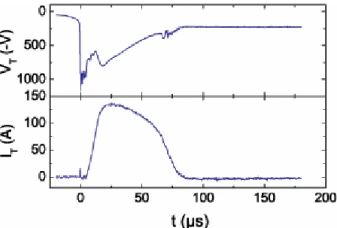
examine the effect of the applied power on film growth. Typical time-traces of the target voltage and current are shown in Fig. 1 for VT = 1000 V. After the initial peak, a decrease
to ~ 700 V was observed as the plasma ignited. A maximum current of 134 A was achieved ~25 µs after the pulse start. The actual VT value, at maximum current, was ~
800 V, resulting in a peak power of ~100 kW, corresponding to a peak power density of ~5 kWcm-2 averaged over the full target surface. The time-average target power was 150 W resulting in a low thermal load of the target.
Fig. 1. Time evolution of the negative target voltage, VT, and the target current, IT, for an
Ar discharge and a Ta target .
The change in deposition rate (Rd) was investigated as a function of the inclination
angle of the substrate for both HIPIMS and dcMS. The dcMS films were grown using a power equal to the average power used for HIPIMS. The HIPIMS depositions were made using a VT of 1000 V. Films were grown with the two techniques using a fixed Vb of 10
V. Depending on the deposition rates, films were grown with thicknesses verying between 0.5 and 1 µm. Fig. 2 shows the obtained deposition rates for dcMS and HIPIMS on samples with different inclination angles. For samples grown facing the target surface (at 0° inclination angle), the deposition rate were 12 and 30 nm min-1 for HIPIMS and dcMS, respectively. For substrates placed at a large angle (>90°) with respect to the target surface, Rd decreased. However, dcMS suffered from a significantly larger decrease in Rd
than HIPIMS as demonstrated in Fig. 2. It is seen that for HIPIMS films grown at a 90° inclination angle, Rd dropped to about 42 % of the value measured at the inclination angle
of 0°. At an even larger inclination angle of 180°, i.e., the substrate surface hidden from the target, Rd decreased to 19 %. The corresponding values for dcMS showed that Rd
Fig 2. Normalized deposition rates measured for films grown by HIPIMS and dcMS.
In order to study the phase content of the deposited films, XRD measurements were performed on both dcMS and HIPIMS grown films. Films were deposited by dcMS with an average power of 150 W, on substrates facing the target surface (0° inclination), at the different negative substrate bias voltages of 10, 30, 50, 70, and 90 V. The resulting X-ray diffractograms (not shown here) exhibited β-Ta (002) peaks for all bias values. However, for 50 V< Vb ≤ 90 V, an additional low-intensity bcc-Ta (110) peak was
observed.
Films were also grown with HIPIMS using the same average power and deposition geometry as in dcMS (VT = 740 V, 0° inclination), and using the Vb values as
for the dcMS films. As seen in the θ−2θ X-ray diffractograms (Fig. 3) the phase formation depends on the applied substrate bias. In all scans, it is observed that the β-Ta (002) peak is shifted to the left (to larger lattice spacing) compared to expected bulk value of 33.69° [18] for all films, which might be due to the ion bombardment of the growing surface that resulted in strained films. It is further observed that for Vb = 70 V the β-Ta
(002) peak disappeared almost completely and the bcc-Ta (110) peak is the dominant peak in the XRD spectrum. For the higher negative substrate bias value investigated (Vb =
90 V), the β-Ta phase is again present, now with the β-Ta (002) peak further left shifted and with a shoulder at the nominal β-Ta (002) angle. In order to quantify the bcc phase content in the films, the XRD intensity ratio Ir=Ibcc/(Ibcc+Iβ), defined as the intensity ratio
between the bcc-Ta (110) peak intensity and the sum of the bcc-Ta (110) and β-Ta (002) peak intensities, was determined. This is shown in Table I, where it can be seen that Ir
was 98 % for the film grown with Vb=70 V. For the other Vb values, β-Ta (002) was the
dominant peak and Ir was 1 % or lower.
Fig. 3 X-ray diffractograms for Ta films grown at different substrate bias voltages, on substrates facing the target surface, using HIPIMS with VT = 740 V and PAr = 0.67 Pa.
The resistivity measurements, also presented in Table 1, showed that the sample deposited with Vb = 70 V had the lowest resistivity value, 32 µΩcm, consistent with
typical bcc-Ta values in the range of 15 to 50 µΩcm [4-5, 7, 9-10]. For the other samples, the resistivity was found to be much higher (110 < ρ < 260 µΩcm), in
agreement with the expected values of 150 to 210 µΩcm for β-Ta films [3-5]. A bias voltage window for growth of the bcc-Ta is, thus, demonstrated.
Table I. XRD intensity ratios (Ir = Ibcc/(Ibcc+Iβ)) and resistivity values (ρ) for samples
facing the target surface, using HIPIMS with VT = 740 V.
Vb (V) Ir (%) ρ (µΩcm) 90 <0.1 260 70 98 32 50 1 112 30 <0.1 238 10 <0.1 202
Figure 4a shows X-ray diffractograms of samples deposited with higher target voltage (VT=1000 V). It is observed that the bcc-Ta (110) peak becomes dominating for
Vb=30 V, which is 40 V lower than the bias voltage needed when a target voltage of 740
V was used. The intensity ratios are summarized in Table II together with the corresponding resistivity values.
The phase composition was also investigated for substrates placed at different angles with respect to the target surface (for VT=1000 V). Figures 4b and 4c show
X-ray diffractograms of Ta films grown at the respective inclination angles of 90 and 135°. bcc-Ta (110) and β-Ta (002) peaks are comparable for the film deposited at 90° with Vb = 30 V, while at Vb = 50 V the bcc-Ta (110) peak dominated. In Fig 4c (135°
inclination), the bcc-Ta (110) peak dominates already at a Vb of 10 V. An increase to
observed for the inclination angle of 180° (not shown). The intensity ratios and the resistivity values obtained for these films are presented in Table II, where it is shown that when bcc-Ta is the dominating phase in the film, ρ is low, while the opposite is true for films that showed mainly β-Ta peaks.
Fig. 4. X-ray diffractograms for samples grown with VT = 1000 V at (a) 0°, (b) 90°,
and (c) 135°.
4 Discussion
XRD showed that all samples grown by dcMS resulted in pure β-Ta films for Vb ≤ 50 V, and a mixture predominantly consisting of β-Ta but with a minority
component of bcc-Ta for higher Vb. This is consistent with Catania et al. [5], who
reported that the bcc phase was not obtained without etching of the natural oxide of the Si substrates. Moreover, other workers [3, 4, 8, 9] demonstrated that the growth of pure bcc-Ta required removal of the native oxide prior to deposition on Si substrates. In the present work, Ta films grown on Si substrates using HIPIMS show the bcc phase without extra cleaning steps. This is possible within a substrate-bias window, and depends on the growth conditions (target voltage and inclination angle of the
substrate). For example, an increase in VT from 740 to 1000 V led to growth of
bcc-Ta at a lower Vb value – a decrease from 70 V to 30 V. Many researchers have
studied the growth of bcc-Ta on Si substrates [2-9] and have shown that stresses induced by ion bombardment can influence the structure of the deposited Ta film. The HIPIMS discharge is highly ionized and a large fraction of the ions bombarding the growing film consists of ions of the sputtered material [19]. This leads to a very efficient momentum transfer to the growth surface due to the mass match between the projectile and the target (the growing film surface). This effect is, especially evident in sputter deposition of heavy elements, such as Ta, by using the relatively light Ar as the sputtering gas. The existence of a window can be understood from the fact that for low energies insufficient stress is induced in the film, and for high energies a
Table II. Intensity ratios (Ir = Ibcc/(Ibcc+Iβ)) and resistivity values (ρ) for samples
grown at 0, 90, and 135° angles with respect to the target, with VT = 1000 V.
Angle (deg.) Vb (V) Ir (%) ρ (µΩcm) 0 30 10 92 < 0.1 24 138 90 50 30 10 96 51 < 0.1 30 80 180 135 30 10 23 80 130 45
relaxation of the stress may be induced by the ion bombardment. An indication of the latter is exhibited by the broad shoulder that is observed at the position of an unstressed β-Ta (002) peak for a Vb value of 90 V (Fig. 3).
The shift in the observed substrate-bias window with inclination angle can be understood in view of the change in ion-to-neutral ratio that reaches the growing surface. For an increasing inclination angle, a reduced number of neutral deposition atoms will reach the substrate. However, the reduction of ionized deposition species will be less pronounced since the negative substrate bias will maintain a flux of ions to the substrate. This results in an increased ion bombardment in relation to the deposition rate as the inclination angle increases.
The importance of a mass match during growth of Ta thin films has also been shown by Dalla Torre et al. [20] and Ino et al. [9], who showed that a more efficient momentum transfer to the growing Ta film is achieved using Xe instead of Ar. An alternative would be to increase the ion bombardment using Ar and a higher Vb [21].
This has the drawback that the penetration depth increases, which can lead to excessive incorporation of Ar in the growing film.
5 Conclusion
It was shown that by using HIPIMS, control of the Ta phase-formation could be obtained. This was achieved by varying the ion bombardment energy as a result of using a negative substrate bias. A large fraction of the bombarding species consists of ions of the film material itself, which ensures an efficient momentum transfer between the ions and the films surface. A bias voltage window for deposition of bcc-Ta on Si (with the native oxide present) was realized. The negative substrate bias voltage required for bcc-Ta to form was varying between 10 and 70 V depending on process conditions. One of the factors influencing the required bias value was the inclination angle of the substrate with respect to the target. For 0° inclination angle (substrate facing the target), a negative substrate bias of 70 V was needed to form the bcc phase,
but for increasing angles the bias value needed decreased. This is attributed to an increased Ta ion-to-neutral ratio in the deposition flux as the inclination angle increases.
Acknowledgements
This work was financially supported from the Swedish Foundation for Strategic Research (SSF) and the Swedish Research Council (VR).
References
[1] http://www.webelements.com.
[2] R. Hoogeveen, M. Moske, H. Geisler, and K. Samwer, Thin Solid Films 275 (1996) 203.
[3] L. A. Clevenger, A. Mutscheller, J. M. E. Harper, C. Cabral, Jr., K. Barmak, J. Appl. Phys. 72 (1992) 4918.
[4] D. W. Face, D. E. Prober, J. Vac. Sci. Technol. A 5 (1987) 3408.
[5] P. Catania, J. P. Doyle, J. J. Cuomo, J. Vac. Sci. Technol. A 10 (1992) 3318. [6] N. O. Nnolim, T. A. Tyson, L. Axe, J. Appl. Phys. 93 (2003) 4544.
[7] L. Abelmann, C. Lodder, Thin Solid Films 305 (1997) 1.
[8] B. Window, F. Sharples, N. Savvides, J. Vac. Sci. Technol. A 6 (1988) 2333. [9] K. Ino, T. Shinohara, T. Ushiki, T. Ohmi, J. Vac. Sci. Technol. A 15 (1997)
2627.
[10] T. Ohmi, T. Ichikawa, H. Iwabushi, T. Shibata, J. Appl. Phys. 66 (1989) 4756. [11] V. Kouznetsov, K. Macák, J.M. Schneider, U. Helmersson, I. Petrov, Surf. Coat.
Technol. 122 (1999) 290.
[12] K. Macák, V. Kouznetsov, J. Schneider, U. Helmersson, I. Petrov, J. Vac. Sci. Technol. A 18 (2000) 1533.
[13] J. T. Gudmundsson, J. Alami, U. Helmersson, Appl. Phys. Lett. 78 (2001) 3427. [14] J. Alami, P.O.Å. Persson, J. Böhlmark, J.T. Gudmundsson, D. Music, U.
Helmersson, J. Vac. Sci. Technol. A 23 (2005) 278.
[15] U. Helmersson, M. Lattemann, J. Bohlmark, Arutiun P. Ehiasarian, and J.T. Gudmundsson, Thin Solid Films 513 (2006) 1.
[16] J. T. Gudmundsson, J. Alami, U. Helmersson, Surf. Coat. Technol. 161 (2002) 249.
[17] J. Alami, J. T. Gudmundsson, J. Bohlmark, J. Birch, U. Helmersson, Plasma Sources Sci. Technol. 14 (2005) 525.
[18] Powder Diffraction File, Joint Committee on Powder Diffraction Standards, ASTM, Philadelphia, Pa, year, Card 25-1280.
[19] J. Bohlmark, J. Alami, C. Christou, A. Ehiasarian, U. Helmersson, J. Vac. Sci. Technol. A 23 (2005) 18.
[20] J. Dalla Torre, G. H. Gilmer, D. L. Windt, R. Kalyanaraman, F. H. Baumann, P. L. O'Sullivan, J. Sapjeta, T. D. de la Rubia, M. D. Rouhani, J. Appl. Phys. 94 (2003) 263.